


 |
市場調查報告書
商品編碼
2157090
面陣掃描工業相機:市佔率分析、產業趨勢與統計及成長預測(2026-2031 年)Area-Scan Industrial Camera - Market Share Analysis, Industry Trends & Statistics, Growth Forecasts (2026 - 2031) |
||||||

※ 本網頁內容可能與最新版本有所差異。詳細情況請與我們聯繫。
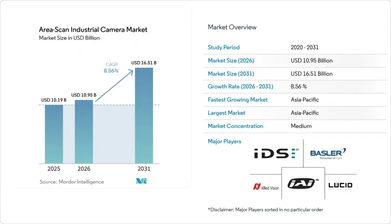
根據 Mordor Intelligence 預測,區域掃描工業相機市場規模將從 2025 年的 101.9 億美元成長到 2026 年的 109.5 億美元,然後在 2031 年達到 165.1 億美元,2026 年至 2031 年的複合年成長率為 8.56%。
全球區域掃描工業相機市場趨勢與洞察
擴大自動化品質檢測
隨著工廠自動化技術的進步,生產線上部署的面陣掃描相機數量不斷增加。在高產能工廠中,人工檢測在成本、一致性和安全性方面都存在問題。 2024年底,全球工業運作數量將達到466.4萬台,較去年同期成長9%。亞太地區佔2024年新增機器人部署量的74%,其中24%應用於電子產業。在視覺軟體領域,使用者對動態範圍和影格速率的要求越來越高,這可能會使老舊相機在計劃更換週期之前成為阻礙因素。 2026年8月,AAEON展示了一款晶圓偵測系統,該系統將工業相機與NVIDIA Jetson Orin NX邊緣模組結合。這種整合系統可以滿足晶圓廠和物流設施在面陣掃描工業相機市場中不斷升級的需求。
半導體和電子製造業的擴張
隨著半導體產能的擴張,晶圓檢測、晶片分選和先進封裝測量所需的成像系統日益成長。 2025年3月,台積電宣佈在美國的投資計畫將達到1,650億美元,其中包括三座製造工廠和兩座先進封裝工廠。這些項目推動了對用於日益精密生產過程的設備的需求。三星電子位於德克薩斯州市的工廠已於2026年開始採用極紫外光刻(EUV)技術進行量產,並計劃在同一地點建造第二座晶圓廠。台積電正在使用NVIDIA Metropolis和NVIDIA TAO Toolkit進行視覺人工智慧缺陷分類。這些工具可以減少因製程條件變化而需要重複標註和重新訓練的情況。因此,晶圓廠的量產啟動時間表仍然是服務於面掃描工業相機市場的供應商的關鍵因素。
高昂的系統整合和應用工程成本
在複雜的檢測專案中,系統整合成本可能遠遠超出相機硬體本身的成本。安裝工作包括鏡頭、照明、校準、軟體配置以及分類參考影像庫。這些工作需要特定應用領域的專業知識,而許多中型製造商恰恰缺乏這方面的內部資源。食品、飲料、包裝和物流行業的企業尤其容易受到這種成本結構的影響。製藥和醫療設備專案可能需要根據美國FDA 21 CFR Part 11和歐盟附件11的要求進行額外的驗證。提供工廠校準系統和預驗證軟體配置的供應商可以減輕客戶現場的工作量。這種方法有助於在價格敏感的面部掃描工業相機市場推廣應用。
細分市場分析
到2025年,CMOS相機將佔據面陣掃描工業相機市場78.64%的佔有率。這一地位得益於全局百葉窗設計的不斷改進。 CMOS相機為工業用戶提供了成本、速度和影像性能的完美結合。SONY的Pregius S背照式(BSI)感測器可在高影格速率下實現寬動態範圍和低讀出雜訊。 CCD感測器在對低光照靈敏度和固定模式雜訊抑制要求尤為重要的領域中仍發揮關鍵作用。這些應用包括紫外光掩模檢測、特定的科學測量工作流程以及小眾天文成像。主要感測器製造商正在將產能轉向CMOS,導致CCD產品的市場佔有率下降。 「其他感測器技術」類別預計到2031年將以9.16%的複合年成長率成長。這包括用於電動車電池水分分析和半導體晶圓測量等應用的短波紅外線和擴展近紅外線感測器。這些感測器可以對標準矽基 CMOS 系統無法有效檢測的材料層和介電薄膜進行成像。
CMOS產品類別中面掃描工業相機的市場規模持續反映該技術的獨特需求。捲簾百葉窗相機適用於對成本敏感且允許存在運動失真的自動化應用。另一方面,全域百葉窗相機對於偵測運動部件至關重要,因為此類應用需要無失真影像。因此,全局百葉窗產品在中高速偵測單元中發揮關鍵作用。此外,半導體和電動車電池的缺陷分類系統需要像素級一致的影像品質。因此,產品線正向平均售價較高的全域百葉窗傾斜。與感測器製造商保持密切合作關係的供應商可以從這種產品線轉變中獲益。 2026年7月,IDS擴展了其符合IP69K標準的uEye FA產品線,將配備SONYSTARVIS 2捲簾百葉窗感測器的型號數量從200萬像素增加到1250萬像素。除了能夠承受惡劣環境外,這些新產品還具有更高的近紅外線靈敏度和高動態範圍(HDR)功能。這些特性可應用於食品和製藥業,在這些行業中,可清洗性和影像品質都非常重要。
預計到2031年,1,200萬像素及以上相機市場將以9.18%的複合年成長率成長。半導體製造廠、顯示器製造商和電動車電池工廠需要在保持生產線滿載運轉的同時,實現精細的成像。這些環境要求相機能夠在廣闊的偵測區域內識別微米級缺陷。 2026年3月,Vieworks發布了VPS-245MX2,該相機具有2.45億像素解析度和珀爾帖冷卻技術。這款相機專為平板顯示器、印刷電路板和半導體元件的檢測而設計。冷卻功能有助於在高解析度下運作中保持感測器的穩定性。高解析度配置也需要相應的介面頻寬、儲存容量和處理能力。面部掃描工業相機市場正透過為要求更高的檢測系統設計的產品來滿足這一需求。即使在低像素系統無法提供足夠的覆蓋範圍或詳細資訊的情況下,高解析度相機也能支援精確的影像擷取。
截至2025年,像素低於500萬的相機佔據了臉部掃描工業相機市場44.21%的佔有率。這一佔有率反映了其在食品、飲料、包裝和物流等行業的檢測應用中的顯著部署。這些應用大多不需要半導體製造中使用的高解析度。 5-1200萬像素等級的相機廣泛應用於汽車車體檢測、藥品泡殼包裝檢驗和組裝指導。此解析度範圍在成本最佳化的多相機系統中實現了影像細節和處理負載之間的平衡。因此,產品選擇取決於檢測任務和可用的系統基礎設施。高解析度型號並非在所有應用中都能取代低解析度型號;相反,它們作為一種高級選項,用於滿足生產對捕捉細節缺陷的需求。這導致不同解析度範圍內的替代模式各不相同。供應商需要提供能夠滿足標準檢測需求以及高解析度應用的產品系列。
區域分析
預計到2025年,亞太地區將佔據區域掃描工業相機市場43.77%的佔有率,並在2031年之前以9.58%的複合年成長率持續成長。中國在該地區擁有強大的電子設備組裝產能。韓國的半導體和平面顯示器製造業務蓬勃發展。台灣地區透過其電路基板和先進封裝的供應鏈支撐著市場需求。韓國的需求主要集中在三星和SK海力士的記憶體和邏輯裝置製造廠。台灣是半導體設備和電路基板生產的重要群聚。印度也正透過基於生產連結獎勵計畫(PLI)計畫的產業現代化,從小規模的基礎不斷擴大。這些生產基地使亞太地區成為區域掃描工業相機市場最大的需求區域。
北美和歐洲分別是第二和第三大區域市場。在北美,根據《晶片與科學法案》(CHIPS and Science Act)提出的2026年資金籌措提案已覆蓋16個州,總額超過320億美元。台積電和三星新建工廠正在推動對精密檢測設備的需求。到了2025年,美國部署的工業機器人數量增加11%,達到38,000台。食品業的機器人部署量成長了30%,需求範圍也擴展到半導體應用之外。德國憑藉其汽車供應鏈和機器視覺製造地在歐洲扮演核心角色。 Basler在2026年上半年的中期報告中指出,與去年同期相比,訂單成長了59%,銷售額成長了36%。歐盟的《人工智慧法案》(AI Act)也對採購計畫產生了影響,買家要求使用經過認證且可解釋的檢測軟體。
南美洲、中東和非洲是區域掃描工業相機市場中規模最小的幾個區域。在巴西,汽車組裝和農產品加工是推動市場需求的主要因素。沙烏地阿拉伯和阿拉伯聯合大公國在化學、食品製造和國防生產領域率先採用了機器視覺技術。南非和埃及的製藥和食品加工企業需要具備出口合規能力,因此對機器視覺的需求也較高。硬體價格和工業網路基礎設施的改善降低了基礎系統的進入門檻。對於複雜的部署而言,本地系統整合能力仍然至關重要。此外,全球供應商需要區域支援網路來協助多相機部署。這些因素將影響這些小規模區域市場的長期商業機會。
其他好處:
- Excel格式的市場預測(ME)表
- 3個月的分析師支持
目錄
第1章:引言
- 研究假設和市場定義
- 調查範圍
第2章:調查方法
第3章執行摘要
第4章 市場狀況
- 市場概覽
- 市場促進因素
- 擴大自動化品質檢測
- 半導體和電子製造業的擴張
- 擴大人工智慧驅動的機器視覺的應用
- 對高解析度和高速影像擷取的需求
- 零缺陷製造的要求
- 利用相機級處理減少偵測延遲
- 市場限制因素
- 高昂的系統整合成本與應用工程成本
- 缺乏機器視覺整合技能
- 感測器和介面過時風險
- 多攝影機系統的資料速率、儲存和熱性能方面的限制
- 宏觀經濟因素對市場的影響
- 產業價值鏈分析
- 監理情勢
- 技術展望
- 波特五力分析
第5章 市場規模與成長預測
- 感測器技術
- CMOS
- CCD
- 其他感測器技術
- 通過決議
- 低於500萬像素
- 5-1200萬像素
- 1200萬像素或以上
- 透過介面標準
- GigE Vision
- USB3 Vision
- Camera Link
- CoaXPress
- 其他介面標準
- 按最終用戶行業分類
- 電子和半導體
- 汽車和電動車電池
- 食品/飲料
- 藥品和醫療保健
- 物流和倉儲
- 包裝/印刷
- 航太/國防
- 其他終端用戶產業
- 按地區
- 北美洲
- 美國
- 加拿大
- 墨西哥
- 南美洲
- 巴西
- 阿根廷
- 其他南美國家
- 歐洲
- 德國
- 英國
- 法國
- 義大利
- 其他歐洲國家
- 亞太地區
- 中國
- 日本
- 韓國
- 台灣
- 印度
- 其他亞太國家
- 中東
- 土耳其
- 沙烏地阿拉伯
- 阿拉伯聯合大公國
- 其他中東國家
- 非洲
- 南非
- 埃及
- 北美洲
第6章 競爭情勢
- 市場集中度
- 策略趨勢
- 市佔率分析
- 公司簡介
- Basler AG
- Allied Vision Technologies GmbH
- IDS Imaging Development Systems GmbH
- JAI A/S
- Emergent Vision Technologies Inc.
- LUCID Vision Labs, Inc.
- Vieworks Co., Ltd.
- Adimec Advanced Image Systems BV
- IMPERX, Inc.
- Teledyne Vision Solutions
- Baumer Group
- Teledyne FLIR
- The Imaging Source Europe GmbH
- Toshiba Teli Corporation
- Alkeria Srl
- Photonfocus AG
- Cognex Corporation
- AOS Technologies AG
- Zhejiang Huaray Technology Co., Ltd.
- Hikrobot Co., Ltd.
- Beijing Daheng Image Vision Co., Ltd.
第7章 市場機會與未來展望
According to Mordor Intelligence, the area-scan industrial camera market size is expected to grow from USD 10.19 billion in 2025 to USD 10.95 billion in 2026, and is forecast to reach USD 16.51 billion by 2031, at an 8.56% CAGR over 2026-2031.
Global Area-Scan Industrial Camera Market Trends and Insights
Expansion of Automated Quality Inspection
Factory automation is increasing the installed base of area-scan cameras across production lines. Manual inspection creates cost, consistency, and safety concerns in high-throughput facilities. The global operational stock of industrial robots reached 4,664,000 units at the end of 2024, up 9% from the prior year. Asia-Pacific accounted for 74% of new robot deployments in 2024, and electronics represented 24% of installations. Vision software is raising expectations for dynamic range and frame rate, which can make older cameras a constraint before planned replacement dates. In August 2026, AAEON demonstrated a wafer inspection system that combined an industrial camera with an NVIDIA Jetson Orin NX edge module. These integrated systems can support recurring upgrade demand in fabs and logistics facilities within the area-scan industrial camera market.
Semiconductor and Electronics Manufacturing Expansion
New semiconductor capacity requires imaging systems for wafer inspection, die sorting, and advanced packaging metrology. TSMC announced in March 2025 that its planned US investment would reach USD 165 billion, including 3 fabrication plants and 2 advanced packaging facilities. The projects add demand for equipment used during increasingly precise production stages. Samsung Electronics' Taylor, Texas, facility reached EUV first-light production in 2026 and was preparing a second fab at the site. TSMC is using NVIDIA Metropolis and the NVIDIA TAO Toolkit for vision AI in defect classification. These tools reduce the need for repeated labeling and retraining as process conditions change. Fab ramp schedules, therefore, remain important for suppliers serving the area-scan industrial camera market.
High System-Integration and Application-Engineering Costs
Complex inspection projects can require substantially more spending on integration than on camera hardware. Installation work includes lenses, lighting, calibration, software recipes, and classified reference-image libraries. These tasks need application knowledge that many mid-sized manufacturers do not maintain in-house. Food, beverage, packaging, and logistics operators are particularly exposed to this cost structure. Pharmaceutical and medical device projects can require additional validation under FDA 21 CFR Part 11 and EU Annex 11 requirements. Vendors that provide factory-calibrated systems and pre-validated software recipes can reduce work on-site at the customer. This approach can improve adoption in price-sensitive parts of the area-scan industrial camera market.
Other drivers and restraints analyzed in the detailed report include:
- Rising Adoption of AI-Enabled Machine Vision
- Demand for Higher Resolution and Faster Image Acquisition
- Shortage of Machine-Vision Integration Skills
For complete list of drivers and restraints, kindly check the Table Of Contents.
Segment Analysis
CMOS held 78.64% of the area-scan industrial camera market share in 2025. Continuous improvement in global-shutter designs has supported this position. CMOS cameras offer a broad mix of cost, speed, and image performance for industrial users. Sony Pregius S back-side illuminated sensors support high dynamic range and low read noise at elevated frame rates. CCD sensors remain relevant where low-light sensitivity and limited fixed-pattern noise are especially important. These applications include UV photomask inspection, certain scientific metrology workflows, and niche astronomical imaging. Major sensor producers have moved production capacity toward CMOS, reducing the commercial position of CCD products. The other sensor technologies category is projected to expand at a 9.16% CAGR through 2031. It includes short-wave infrared and extended near-infrared sensors for EV battery moisture analysis and semiconductor wafer metrology. These sensors can image through material layers or dielectric films that standard silicon-based CMOS systems cannot inspect effectively.
The area-scan industrial camera market size for CMOS products continues to reflect distinct needs within the technology. Rolling-shutter cameras serve cost-sensitive automation uses where motion distortion is manageable. Global-shutter cameras are necessary for moving parts that require distortion-free images. This makes global-shutter products important in mid-speed and high-speed inspection cells. Semiconductor and EV battery defect classifiers also require consistent pixel-level image quality. The product mix is therefore moving toward global-shutter configurations with higher average selling prices. Suppliers with stronger sensor relationships can benefit as this mix changes. IDS expanded its uEye FA IP69K-rated range in July 2026 with Sony STARVIS 2 rolling-shutter sensors from 2 to 12.5 megapixels. The launch addressed harsh environments while adding near-infrared sensitivity and high dynamic range. Food and pharmaceutical applications can use these capabilities where washdown resistance and image quality both matter.
The above-12-megapixel tier is projected to expand at a 9.18% CAGR through 2031. Semiconductor fabs, display producers, and EV battery plants require detailed images at full line throughput. These settings require cameras capable of identifying micron-scale defects across large inspection areas. Vieworks introduced the VPS-245MX2 in March 2026 with 245-megapixel resolution and thermoelectric Peltier cooling. The camera targeted flat-panel display, PCB, and semiconductor component inspection. Cooling can help maintain sensor stability during sustained, high-resolution operation. Higher-resolution configurations also require matching interface bandwidth, storage capacity, and processing capability. The area-scan industrial camera market responds to this need through products designed for more demanding inspection systems. High-resolution cameras can support precise imaging where lower-pixel-count systems cannot deliver adequate coverage or defect detail.
Below-5-megapixel cameras accounted for 44.21% of the area-scan industrial camera market size in 2025. Their position reflects a large installed base in food, beverage, packaging, and logistics inspection. Many of these applications do not require the resolution used in semiconductor manufacturing. The 5-12-megapixel tier is widely used in automotive body inspection, pharmaceutical blister-pack verification, and assembly guidance. It balances image detail with processing load in cost-optimized multi-camera systems. Product selection, therefore, depends on the inspection task and the available system infrastructure. Higher resolution does not replace lower-resolution models across every application. Instead, it adds a premium option where detailed defect capture supports the production requirement. This creates different replacement patterns across the resolution spectrum. Suppliers need portfolios that cover standard inspection demand alongside high-resolution deployments.
Complete Report Scope:
- By Sensor Technology
- CMOS
- CCD
- Other Sensor Technologies
- By Resolution
- Below 5 Megapixels
- 5-12 Megapixels
- Above 12 Megapixels
- By Interface Standard
- GigE Vision
- USB3 Vision
- Camera Link
- CoaXPress
- Other Interface Standards
- By End-User Industry
- Electronics and Semiconductor
- Automotive and EV Battery
- Food and Beverage
- Pharmaceuticals and Healthcare
- Logistics and Warehousing
- Packaging and Printing
- Aerospace and Defense
- Other End-User Industries
- By Geography
- North America
- United States
- Canada
- Mexico
- South America
- Brazil
- Argentina
- Rest of South America
- Europe
- Germany
- United Kingdom
- France
- Italy
- Rest of Europe
- Asia-Pacific
- China
- Japan
- South Korea
- Taiwan
- India
- Rest of Asia-Pacific
- Middle East
- Turkey
- Saudi Arabia
- United Arab Emirates
- Rest of Middle East
- Africa
- South Africa
- Egypt
- North America
Geography Analysis
Asia-Pacific held 43.77% of the area-scan industrial camera market share in 2025 and is projected to expand at a 9.58% CAGR through 2031. China provides a large capacity for electronics assembly in the region. South Korea has intensive semiconductor and flat-panel fabrication activity. Taiwan supports demand through circuit board and advanced packaging supply chains. South Korea's demand is concentrated around Samsung and SK Hynix memory and logic fabrication facilities. Taiwan is an important integration hub for semiconductor equipment and circuit-board production. India is also expanding from a smaller base through industrial modernization under the Production-Linked Incentive scheme. These production centers make Asia-Pacific the leading demand region for the area-scan industrial camera market.
North America and Europe are the second- and third-largest regional markets. In North America, proposed funding for the CHIPS and Science Act exceeded USD 32 billion across 16 states in 2026. New facilities from TSMC and Samsung are adding demand for precision inspection equipment. US industrial robot installations increased by 11% to 38,000 units in 2025. Food-sector robot adoption increased 30%, broadening demand beyond semiconductor applications. Germany anchors Europe through its automotive supply chain and machine vision manufacturing base. Basler reported that orders increased 59% year over year and revenue increased 36% in its H1 2026 interim report. The EU AI Act is also affecting procurement timelines, with buyers seeking certified and explainable inspection software.
South America, the Middle East, and Africa form the smallest geographic tier in the area-scan industrial camera market. Brazil supports demand through automotive assembly and agri-food processing. Saudi Arabia and the UAE are adding early machine vision installations in chemicals, food manufacturing, and defense production. South Africa and Egypt show demand from pharmaceutical and food-processing operations that need export-compliance capabilities. Hardware prices and industrial network infrastructure can lower the barriers to entry for basic systems. Local systems-integration capability remains important for complex installations. Global suppliers also need regional support networks to service multi-camera deployments. These factors will shape the longer-term opportunity across the smaller regional markets.
- Basler AG
- Allied Vision Technologies GmbH
- IDS Imaging Development Systems GmbH
- JAI A/S
- Emergent Vision Technologies Inc.
- LUCID Vision Labs, Inc.
- Vieworks Co., Ltd.
- Adimec Advanced Image Systems B.V.
- IMPERX, Inc.
- Teledyne Vision Solutions
- Baumer Group
- Teledyne FLIR
- The Imaging Source Europe GmbH
- Toshiba Teli Corporation
- Alkeria S.r.l.
- Photonfocus AG
- Cognex Corporation
- AOS Technologies AG
- Zhejiang Huaray Technology Co., Ltd.
- Hikrobot Co., Ltd.
- Beijing Daheng Image Vision Co., Ltd.
Additional Benefits:
- The market estimate (ME) sheet in Excel format
- 3 months of analyst support
TABLE OF CONTENTS
1 INTRODUCTION
- 1.1 Study Assumptions and Market Definition
- 1.2 Scope of the Study
2 RESEARCH METHODOLOGY
3 EXECUTIVE SUMMARY
4 MARKET LANDSCAPE
- 4.1 Market Overview
- 4.2 Market Drivers
- 4.2.1 Expansion of Automated Quality Inspection
- 4.2.2 Semiconductor and Electronics Manufacturing Expansion
- 4.2.3 Rising Adoption of AI-Enabled Machine Vision
- 4.2.4 Demand for Higher Resolution and Faster Image Acquisition
- 4.2.5 Zero-Defect Manufacturing Requirements
- 4.2.6 Camera-Level Processing for Reduced Inspection Latency
- 4.3 Market Restraints
- 4.3.1 High System-Integration and Application-Engineering Costs
- 4.3.2 Shortage of Machine-Vision Integration Skills
- 4.3.3 Sensor and Interface Obsolescence Risk
- 4.3.4 Data-Rate, Storage, and Thermal Constraints in Multi-Camera Systems
- 4.4 Impact of Macroeconomic Factors on the Market
- 4.5 Industry Value Chain Analysis
- 4.6 Regulatory Landscape
- 4.7 Technological Outlook
- 4.8 Porter's Five Forces Analysis
- 4.8.1 Bargaining Power of Suppliers
- 4.8.2 Bargaining Power of Buyers
- 4.8.3 Threat of New Entrants
- 4.8.4 Threat of Substitutes
- 4.8.5 Intensity of Competitive Rivalry
5 MARKET SIZE AND GROWTH FORECASTS (VALUE)
- 5.1 By Sensor Technology
- 5.1.1 CMOS
- 5.1.2 CCD
- 5.1.3 Other Sensor Technologies
- 5.2 By Resolution
- 5.2.1 Below 5 Megapixels
- 5.2.2 5-12 Megapixels
- 5.2.3 Above 12 Megapixels
- 5.3 By Interface Standard
- 5.3.1 GigE Vision
- 5.3.2 USB3 Vision
- 5.3.3 Camera Link
- 5.3.4 CoaXPress
- 5.3.5 Other Interface Standards
- 5.4 By End-User Industry
- 5.4.1 Electronics and Semiconductor
- 5.4.2 Automotive and EV Battery
- 5.4.3 Food and Beverage
- 5.4.4 Pharmaceuticals and Healthcare
- 5.4.5 Logistics and Warehousing
- 5.4.6 Packaging and Printing
- 5.4.7 Aerospace and Defense
- 5.4.8 Other End-User Industries
- 5.5 By Geography
- 5.5.1 North America
- 5.5.1.1 United States
- 5.5.1.2 Canada
- 5.5.1.3 Mexico
- 5.5.2 South America
- 5.5.2.1 Brazil
- 5.5.2.2 Argentina
- 5.5.2.3 Rest of South America
- 5.5.3 Europe
- 5.5.3.1 Germany
- 5.5.3.2 United Kingdom
- 5.5.3.3 France
- 5.5.3.4 Italy
- 5.5.3.5 Rest of Europe
- 5.5.4 Asia-Pacific
- 5.5.4.1 China
- 5.5.4.2 Japan
- 5.5.4.3 South Korea
- 5.5.4.4 Taiwan
- 5.5.4.5 India
- 5.5.4.6 Rest of Asia-Pacific
- 5.5.5 Middle East
- 5.5.5.1 Turkey
- 5.5.5.2 Saudi Arabia
- 5.5.5.3 United Arab Emirates
- 5.5.5.4 Rest of Middle East
- 5.5.6 Africa
- 5.5.6.1 South Africa
- 5.5.6.2 Egypt
- 5.5.1 North America
6 COMPETITIVE LANDSCAPE
- 6.1 Market Concentration
- 6.2 Strategic Moves
- 6.3 Market Share Analysis
- 6.4 Company Profiles (includes Global Level Overview, Market Level Overview, Core Segments, Financials as available, Strategic Information, Market Rank/Share, Products and Services, Recent Developments)
- 6.4.1 Basler AG
- 6.4.2 Allied Vision Technologies GmbH
- 6.4.3 IDS Imaging Development Systems GmbH
- 6.4.4 JAI A/S
- 6.4.5 Emergent Vision Technologies Inc.
- 6.4.6 LUCID Vision Labs, Inc.
- 6.4.7 Vieworks Co., Ltd.
- 6.4.8 Adimec Advanced Image Systems B.V.
- 6.4.9 IMPERX, Inc.
- 6.4.10 Teledyne Vision Solutions
- 6.4.11 Baumer Group
- 6.4.12 Teledyne FLIR
- 6.4.13 The Imaging Source Europe GmbH
- 6.4.14 Toshiba Teli Corporation
- 6.4.15 Alkeria S.r.l.
- 6.4.16 Photonfocus AG
- 6.4.17 Cognex Corporation
- 6.4.18 AOS Technologies AG
- 6.4.19 Zhejiang Huaray Technology Co., Ltd.
- 6.4.20 Hikrobot Co., Ltd.
- 6.4.21 Beijing Daheng Image Vision Co., Ltd.
7 MARKET OPPORTUNITIES AND FUTURE OUTLOOK
- 7.1 White-Space and Unmet-Need Assessment

 OGI攝影機系統市場:全球市場預測,2026-2032年
 中波紅外線工業相機:市場佔有率分析、產業趨勢與統計及成長預測(2026-2031)
 工業相機市場規模:按類型、感測器類型、應用、地區和預測分類建築攝影機:市場佔有率分析、行業趨勢和統計數據、成長預測(2026-2031)
 2026年全球建築攝影解決方案市場報告
 凸輪端面加工系統市場規模、佔有率和成長分析:按操作技術、系統整合、葉片配置、車輛類型、銷售管道和地區分類 - 產業預測,2026-2033 年全球建築攝影機市場規模、佔有率、趨勢和成長分析報告(2026-2034)
 機器人履帶式攝影系統市場分析及預測(至2035年):依類型、產品類型、服務、技術、組件、應用、最終用戶、功能、安裝類型及解決方案分類2026年全球攝影相機市場報告
 攝影機系統市場規模、佔有率和成長分析(按類型、應用和地區分類)-2026-2033年產業預測