

 |
市場調查報告書
商品編碼
2124819
邏輯積體電路(IC):市場佔有率分析、產業趨勢與統計資料、成長預測(2026-2031)Logic IC (Integrated Circuit) - Market Share Analysis, Industry Trends & Statistics, Growth Forecasts (2026 - 2031) |
||||||

※ 本網頁內容可能與最新版本有所差異。詳細情況請與我們聯繫。
據 Mordor Intelligence 稱,2025 年邏輯 IC 市場價值為 2457.3 億美元,預計到 2031 年將達到 3039.1 億美元,而 2026 年為 2545.8 億美元,預測期(2026-2031 年)的複合成長率為 3.60%。
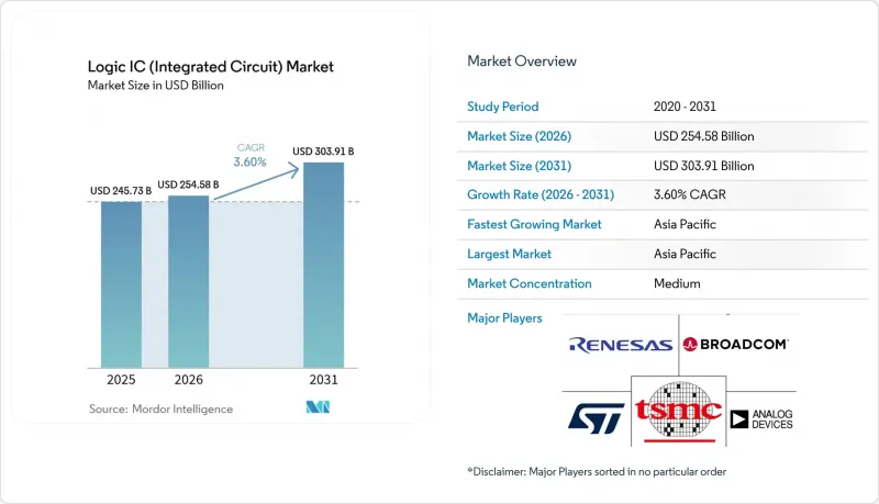
本報告依積體電路類型(數位雙極邏輯、MOS邏輯)、技術節點(45nm及以上、20-44nm、10-19nm、7-9nm及5nm以下)、晶圓尺寸(150mm以下、200mm及300mm)、應用(家用電子電器、汽車、IT及電信基礎設施、電腦及北美地區、工業分類、中心、歐洲、工業系統分類)及歐洲、工業系統分類、電腦及北美地區、工業系統分類)。
全球邏輯積體電路(IC)市場趨勢與洞察
邊緣人工智慧推動了對超低延遲邏輯積體電路的需求。
邊緣人工智慧的普及已將推理工作負載從雲端資料中心轉移到需要亞毫秒響應時間的裝置處理器。 2024年,BrainChip的「Akida Pico」實現了0.35 TOPS/W的能源效率比,與傳統DSP相比,功耗降低了90%。 EdgeCortix預測,到2027年,這類邊緣人工智慧設備將佔人工智慧半導體銷售額的40%,因為自主機器人、無人機和穿戴式裝置無法容忍50-100毫秒的雲端延遲。即時感知系統要求影像和雷射雷達資料在10毫秒內完成處理,促使邏輯積體電路設計人員將目光轉向稀疏神經網路加速器。 5G邊緣運算與人工智慧推理的融合將在2028年為特種邏輯晶片創造150億美元的市場機遇,進一步鞏固邏輯積體電路市場的成長動能。
汽車ADAS和網域控制器需要高度可靠的邏輯。
在軟體定義車輛 (SDV) 中,多個電子控制單元 (ECU) 被整合到一個符合 ISO 26262 安全標準的集中式網域控制站。 2024 年,瑞薩電子發布了「R-Car V4H」SoC,該晶片採用 28nm 工藝,整合了即時控制、人工智慧推理和網路安全功能。大陸集團的 ADCU 系列採用 AEC-Q100 等級元件實現了 171 TOPS 的運算能力,而特斯拉的「硬體 4.0」平台則以 1000 TOPS 為目標,這意味著四年內實現了十倍的飛躍。因此,汽車邏輯 IC 的價格比消費級同類產品上漲了 3-5 倍,即使在成熟製程節點的通縮週期中,也能維持強勁的利潤率。可靠性的重要性推動了長期供應合約的簽訂,增強了客戶鎖定,並支撐了邏輯 IC 市場的整體需求。
極紫外線(EUV)微影術設備供應瓶頸
ASML 仍然是 EUV 設備的唯一供應商,每台高數值孔徑 (High-NA) 設備售價高達 3.5 億美元,交貨週期長達 18 個月。產能限制阻礙了 3 奈米以下製程產能的擴張。儘管三大晶圓代工廠到 2030 年需要超過 200 台設備,但 ASML 的年產量卻被限制在 60 台左右。英特爾的 18A藍圖依賴高數值孔徑設備的供應,這使得風險生產推遲到了 2027 年。由於 3 奈米以下製程的套刻誤差導致良率下降,加劇了產能短缺,在新一代設備成熟之前,邏輯 IC 市場的供應端一直受到限制。
細分市場分析
預計到2025年,專用MOS邏輯晶片將佔邏輯晶片市場佔有率的32.12%,並在2031年之前以5.74%的複合年成長率成長。這一細分市場的成長主要得益於人工智慧加速器,它們能夠彌補通用處理器的效率不足。 Meta公司在2024年發布的關於乘加陣列的資訊顯示,與傳統的純量核心相比,乘加陣列在特定應用中可以實現10倍的吞吐量提升。隨著超大規模資料中心業者將客製化晶片藍圖納入內部開發,人工智慧MOS元件的邏輯晶片市場規模預計將以高於整體市場的速度成長。
消費性電子產品和動力傳動系統模組對MOS通用邏輯、閘陣列和驅動器/控制器的需求持續成長。汽車電氣化進一步擴大了對控制電池系統的MOS驅動IC的需求。同時,數位雙極邏輯在抗輻射航太電路領域保持其獨特的價值。三星將於2024年發布的非二進位AI晶片進一步強化了專用邏輯的發展趨勢,並預示著供應商環境將進一步細分。
受人工智慧、高效能運算以及能夠承受晶圓成本飆升的高階行動應用的推動,5nm及其子節點晶片市場預計到2031年將以11.08%的複合年成長率成長。隨著先進封裝技術的日益普及,5nm及其子節點相關的邏輯積體電路市場規模預計將大幅成長。同時,20-44nm製程晶片在2025年將維持37.02%的市場佔有率,主要服務於資訊娛樂、工業控制以及對成本敏感的物聯網應用。台積電計畫於2024年實現3nm製程的量產,其整合密度比5nm製程高出60%,但高昂的價格限制了其應用範圍,目前僅限於旗艦產品。
10-19奈米製程節點彌合了性價比差距,並被應用於中階智慧型手機和邊緣閘道器。 45奈米以上製程節點則成為馬達驅動器和感測器等高度依賴類比電路的系統的量產選擇。中國的產業政策投入數十億美元用於14奈米和28奈米製程的自主研發,增強了中端製程節點的產能,而此時全球的關注點已轉向2-3奈米製程。因此,邏輯積體電路市場呈現兩極化的格局:產量集中在成熟製程節點,而利潤來源則集中在尖端製程節點。
區域分析
預計到2025年,亞太地區將佔全球銷售額的33.05%,年複合成長率達4.12%。這主要得益於台灣地區64.9%的晶圓代工市場佔有率以及中國大陸晶圓廠的快速擴張。儘管政治摩擦導致跨國公司在海峽兩岸都採取雙供應商策略,台積電在3奈米和早期2奈米製程方面仍保持著技術領先地位。中國計劃在2030年投資1,430億美元,將晶圓代工能力提升至7奈米水平,逐步縮小與最尖端科技競爭對手之間的差距,但目前尚未完全消除這一差距。
在北美,英特爾計劃利用《晶片法案》(CHIPS Act)將其市佔率從2025年的10%提升至2031年的22%。英特爾位於俄亥俄州的工廠將成為該地區最大的新型邏輯半導體製造地,並計劃於2027年開始試生產2奈米製程的產品。美國受惠於對人工智慧加速器、航太和國防微電子產品以及汽車域控制器的需求,但預計到2030年將出現6.7萬名技術純熟勞工的缺口,這對產能擴張構成了風險。
歐洲的戰略圍繞著其在汽車和工業領域的優勢。耗資430億歐元(約505.6億美元)的「晶片法案」充分利用了德國和法國的叢集,並設定了2030年佔全球晶片產量20%的目標。英飛凌和義法半導體將其業務轉型至針對電動交通和智慧工廠最佳化的邏輯平台,在這些領域,功率和安全性至關重要。日本、以色列和海灣國家也進行了類似的投資,旨在奠定基礎,但與東亞、北美和西歐這三大核心區域相比,這些投資規模較小,更多地是作為快速成長的需求區域,而非邏輯整合電路市場的生產中心。
其他好處
- Excel格式的市場預測(ME)表
- 3個月的分析師支持
目錄
第1章:引言
- 研究假設和市場定義
- 調查範圍
第2章:調查方法
第3章執行摘要
第4章 市場狀況
- 市場概覽
- 市場促進因素
- 邊緣人工智慧推動了對超低延遲邏輯積體電路的需求。
- 汽車ADAS和網域控制器需要高度可靠的邏輯
- 政府主導的先進節點晶圓廠獎勵(例如,美國的《晶片法案》、中國的積體電路基金)
- 透過 3D 和 2.5D 異質整合,提高每個封裝的邏輯 IC 容量。
- 需要亞微瓦邏輯電路的電池供電型物聯網節點的快速普及。
- 市場限制因素
- 極紫外線(EUV)微影術設備的瓶頸
- 5奈米以下設計的非重複性工程費用和智慧財產權授權成本不斷上漲。
- 對EDA和製程設備的出口地緣政治限制
- 全球先進邏輯設計與檢驗領域人才短缺
- 價值鏈分析
- 監管和技術展望
- 波特五力分析
- 投資分析
- 宏觀經濟因素對市場的影響
第5章 市場規模與成長預測
- 依積體電路類型
- 數位雙極邏輯
- MOS邏輯
- 一般
- 閘陣列
- 驅動控制器
- 標準電池
- 獨家的
- 依技術節點
- 45奈米或以上
- 20~44nm
- 10~19nm
- 7~9nm
- 5奈米或更小
- 按晶圓尺寸
- 150毫米或更小
- 200mm
- 300mm
- 透過使用
- 家用電子電器
- 車
- 資訊科技和通訊基礎設施
- 電腦資料中心
- 工業自動化
- 醫療和保健設備
- 其他
- 按地區
- 北美洲
- 美國
- 加拿大
- 墨西哥
- 歐洲
- 德國
- 法國
- 英國
- 北歐的
- 其他歐洲國家
- 亞太地區
- 中國
- 台灣
- 韓國
- 日本
- 印度
- 亞太其他地區
- 南美洲
- 巴西
- 墨西哥
- 阿根廷
- 南美洲其他地區
- 中東和非洲
- 中東
- 沙烏地阿拉伯
- 阿拉伯聯合大公國
- 土耳其
- 其他中東國家
- 非洲
- 南非
- 其他非洲地區
- 中東
- 北美洲
第6章 競爭情勢
- 市場集中度
- 策略趨勢
- 市佔率分析
- 公司簡介
- Intel Corporation
- Taiwan Semiconductor Manufacturing Company Limited(TSMC)
- Samsung Electronics Co., Ltd.
- Texas Instruments Incorporated
- NXP Semiconductors NV
- STMicroelectronics NV
- onsemi(ON Semiconductor Corp.)
- Renesas Electronics Corporation
- Analog Devices, Inc.
- Broadcom Inc.
- Infineon Technologies AG
- Microchip Technology Incorporated
- Toshiba Electronic Devices & Storage Corp.
- Skyworks Solutions, Inc.
- ROHM Co., Ltd.
- Marvell Technology, Inc.
- MediaTek Inc.
- Silicon Laboratories Inc.
- Lattice Semiconductor Corporation
- Dialog Semiconductor Plc(Renesas)
第7章 市場機會與未來展望
According to Mordor Intelligence, the logic IC market size was valued at USD 245.73 billion in 2025 and estimated to grow from USD 254.58 billion in 2026 to reach USD 303.91 billion by 2031, at a CAGR of 3.60% during the forecast period (2026-2031).
This report is Segmented by IC Type (Digital Bipolar Logic, and MOS Logic), Technology Node (>=45 Nm, 20-44 Nm, 10-19 Nm, 7-9 Nm, and <=5 Nm), Wafer Size (<=150 Mm, 200 Mm, and 300 Mm), Application (Consumer Electronics, Automotive, IT and Communication Infrastructure, Computer/Data-Center, Industrial and Automation, and More), and Geography (North America, Europe, Asia-Pacific, South America, and Middle East and Africa).
Global Logic IC (Integrated Circuit) Market Trends and Insights
Edge-AI-driven demand for ultra-low-latency logic ICs
Edge AI deployment shifted inference workloads away from cloud data centers toward on-device processors that required sub-millisecond reaction times. In 2024, BrainChip's Akida Pico delivered 0.35 TOPS/W, cutting power budgets by 90% versus conventional DSPs. EdgeCortix projected that such edge AI devices could capture 40% of AI semiconductor revenue by 2027, as autonomous robots, drones, and wearables cannot tolerate 50-100 ms cloud latency. With real-time perception systems needing image and LiDAR data processed inside 10 ms, logic IC designers pivoted to sparse neural-network accelerators. The convergence of 5G edge computing and AI inference created a USD 15 billion serviceable opportunity for specialized logic by 2028, reinforcing the growth trajectory of the logic IC market.
Automotive ADAS and domain controllers require high-reliability logic.
Software-defined vehicles consolidated multiple ECUs into centralized domain controllers subject to ISO 26262 safety grades. In 2024, Renesas introduced the R-Car V4H SoC that fused real-time control, AI inference, and cybersecurity on a 28 nm die. Continental's ADCU family hit 171 TOPS with AEC-Q100 grade parts, and Tesla's Hardware 4.0 platform targeted 1,000 TOPS, demonstrating a ten-fold leap in four years. Automotive logic ICs therefore carried 3-5 x price uplifts over consumer equivalents, sustaining margin resilience even in a deflationary cycle for mature nodes. The reliability imperative drove long-lifecycle supply contracts that deepened customer lock-in and underpinned demand across the logic IC market.
Extreme-UV lithography equipment bottlenecks
ASML remained the sole supplier of EUV tools, and each High-NA machine cost USD 350 million while requiring 18 months to deliver. Limited throughput held back sub-3 nm capacity: the big three foundries needed more than 200 units by 2030, but ASML's annual output plateaued near 60 systems. Intel's 18A roadmap hinged on High-NA availability, pushing risk production toward 2027. Yield loss from sub-nanometer overlay error compounded capacity strain, curbing the supply side of the logic IC market until new tool generations matured.
Other drivers and restraints analyzed in the detailed report include:
- Government-backed advanced-node fab incentives
- 3D/2.5D heterogeneous integration accelerating logic IC content per package
- Escalating <5 nm design NRE and IP licensing costs
For complete list of drivers and restraints, kindly check the Table Of Contents.
Segment Analysis
MOS special-purpose logic captured a 32.12% share of the logic IC market in 2025 and is on course for a 5.74% CAGR until 2031. This branch is spearheaded by AI accelerators that offset the inefficiency of general-purpose processors. Meta's 2024 disclosures of multiply-accumulate arrays showcased application-specific throughput gains of 10x over traditional scalar cores. The logic IC market size for AI-oriented MOS devices is projected to climb at a rate faster than the aggregate market as hyperscalers internalize custom silicon roadmaps.
Demand for MOS general-purpose logic, gate arrays, and drivers/controllers grew steadily inside consumer electronics and power-train modules. Automotive electrification injected extra volume into MOS driver ICs that oversee battery systems. Meanwhile, digital bipolar logic held niche value in radiation-hardened aerospace circuits. Samsung's 2024 rollout of non-binary AI chips reinforced the trend toward purpose-built logic, pointing to an increasingly segmented supplier landscape.
The <=5 nm cohort expanded at 11.08% CAGR through 2031, energised by AI, HPC, and premium mobile applications willing to absorb elevated wafer costs. The logic IC market size associated with <=5 nm nodes is expected to jump in tandem with advanced packaging adoption. At the same time, the 20-44 nm class retained a 37.02% share in 2025, supporting infotainment, industrial control, and cost-sensitive IoT. TSMC's 3 nm ramp in 2024 delivered 60% higher density relative to 5 nm, yet the premium contained its use to flagship products.
Nodes at 10-19 nm bridged cost and performance gaps, serving midrange smartphones and edge gateways. The >=45 nm bracket persisted as a high-volume option for analog-heavy systems in motor drives and sensors. China's industrial policy channelled billions toward 14 nm and 28 nm self-reliance, reinforcing mid-node capacity even as global attention gravitated to 2-3 nm. Consequently, the logic IC market displayed a bifurcated profile: volume resided in mature nodes, but profit pools coalesced at the leading edge.
Complete Report Scope:
- By IC Type
- Digital Bipolar Logic
- MOS Logic
- General-Purpose
- Gate Arrays
- Drivers / Controllers
- Standard Cells
- Special-Purpose
- By Technology Node
- >= 45 nm
- 20-44 nm
- 10-19 nm
- 7-9 nm
- <= 5 nm
- By Wafer Size
- <=150 mm
- 200 mm
- 300 mm
- By Application
- Consumer Electronics
- Automotive
- IT and Communication Infrastructure
- Computer / Data-Center
- Industrial and Automation
- Medical and Healthcare Devices
- Other Applications
- By Geography
- North America
- United States
- Canada
- Mexico
- Europe
- Germany
- France
- United Kingdom
- Nordics
- Rest of Europe
- Asia-Pacific
- China
- Taiwan
- South Korea
- Japan
- India
- Rest of Asia-Pacific
- South America
- Brazil
- Mexico
- Argentina
- Rest of South America
- Middle East and Africa
- Middle East
- Saudi Arabia
- United Arab Emirates
- Turkey
- Rest of Middle East
- Africa
- South Africa
- Rest of Africa
- Middle East
- North America
Geography Analysis
Asia-Pacific commanded 33.05% of 2025 revenue and advanced at 4.12% CAGR, anchored by Taiwan's 64.9% foundry share and China's accelerated build-out of domestic fabs. Political friction prompted multinational customers to dual-source outside the Taiwan Strait, yet TSMC retained technical leadership at 3 nm and early 2 nm tape-outs. China invested USD 143 billion up to 2030 to elevate its foundry capability toward 7 nm, gradually narrowing but not closing the gap with leading-edge peers.
North America used the CHIPS Act to push production share from 10% in 2025 toward 22% by 2031. Intel's Ohio complex represented the largest greenfield logic facility in the region, aimed at 2 nm risk production by 2027. The United States benefited from demand in AI accelerators, aerospace-defence microelectronics, and automotive domain controllers, but a projected shortage of 67,000 skilled workers by 2030 risked hampering the ramp.
Europe positioned itself around automotive and industrial strengths. The EUR 43 billion (USD 50.56 billion) Chips Act set a target of 20% global output by 2030, leveraging clusters in Germany and France. Infineon and STMicroelectronics pivoted toward power and safety-critical logic platforms tailored for electrified transport and smart factories. Parallel investments in Japan, Israel, and the Gulf aimed to gain toeholds but remained subscale relative to the tri-polar core of East Asia, North America, and Western Europe, maintaining their roles as fast-growing demand zones rather than production hearts of the logic IC market.
- Intel Corporation
- Taiwan Semiconductor Manufacturing Company Limited (TSMC)
- Samsung Electronics Co., Ltd.
- Texas Instruments Incorporated
- NXP Semiconductors N.V.
- STMicroelectronics N.V.
- onsemi (ON Semiconductor Corp.)
- Renesas Electronics Corporation
- Analog Devices, Inc.
- Broadcom Inc.
- Infineon Technologies AG
- Microchip Technology Incorporated
- Toshiba Electronic Devices & Storage Corp.
- Skyworks Solutions, Inc.
- ROHM Co., Ltd.
- Marvell Technology, Inc.
- MediaTek Inc.
- Silicon Laboratories Inc.
- Lattice Semiconductor Corporation
- Dialog Semiconductor Plc (Renesas)
Additional Benefits:
- The market estimate (ME) sheet in Excel format
- 3 months of analyst support
TABLE OF CONTENTS
1 INTRODUCTION
- 1.1 Study Assumptions and Market Definition
- 1.2 Scope of the Study
2 RESEARCH METHODOLOGY
3 EXECUTIVE SUMMARY
4 MARKET LANDSCAPE
- 4.1 Market Overview
- 4.2 Market Drivers
- 4.2.1 Edge-AI-Driven Demand for Ultra-Low-Latency Logic ICs
- 4.2.2 Automotive ADAS and Domain Controllers Requiring High-Reliability Logic
- 4.2.3 Government-Backed Advanced-Node FAB Incentives (U.S. CHIPS, China IC Fund)
- 4.2.4 3D/2.5D Heterogeneous Integration Accelerating Logic IC Content per Package
- 4.2.5 Rapid Proliferation of Battery-Powered IoT Nodes Demanding Sub-µW Logic
- 4.3 Market Restraints
- 4.3.1 Extreme-UV Lithography Equipment Bottlenecks
- 4.3.2 Escalating <5 nm Design NRE and IP Licensing Costs
- 4.3.3 Geopolitical Export Controls on EDA and Process Equipment
- 4.3.4 Global Talent Crunch in Advanced Logic Design and Verification
- 4.4 Value Chain Analysis
- 4.5 Regulatory or Technological Outlook
- 4.6 Porter's Five Forces Analysis
- 4.6.1 Bargaining Power of Suppliers
- 4.6.2 Bargaining Power of Buyers
- 4.6.3 Threat of New Entrants
- 4.6.4 Intensity of Competitive Rivalry
- 4.6.5 Threat of Substitutes
- 4.7 Investment Analysis
- 4.8 Impact of macroeconomic factors on the market
5 MARKET SIZE AND GROWTH FORECASTS (VALUE AND VOLUME)
- 5.1 By IC Type
- 5.1.1 Digital Bipolar Logic
- 5.1.2 MOS Logic
- 5.1.2.1 General-Purpose
- 5.1.2.2 Gate Arrays
- 5.1.2.3 Drivers / Controllers
- 5.1.2.4 Standard Cells
- 5.1.2.5 Special-Purpose
- 5.2 By Technology Node
- 5.2.1 >= 45 nm
- 5.2.2 20-44 nm
- 5.2.3 10-19 nm
- 5.2.4 7-9 nm
- 5.2.5 <= 5 nm
- 5.3 By Wafer Size
- 5.3.1 <=150 mm
- 5.3.2 200 mm
- 5.3.3 300 mm
- 5.4 By Application
- 5.4.1 Consumer Electronics
- 5.4.2 Automotive
- 5.4.3 IT and Communication Infrastructure
- 5.4.4 Computer / Data-Center
- 5.4.5 Industrial and Automation
- 5.4.6 Medical and Healthcare Devices
- 5.4.7 Other Applications
- 5.5 By Geography
- 5.5.1 North America
- 5.5.1.1 United States
- 5.5.1.2 Canada
- 5.5.1.3 Mexico
- 5.5.2 Europe
- 5.5.2.1 Germany
- 5.5.2.2 France
- 5.5.2.3 United Kingdom
- 5.5.2.4 Nordics
- 5.5.2.5 Rest of Europe
- 5.5.3 Asia-Pacific
- 5.5.3.1 China
- 5.5.3.2 Taiwan
- 5.5.3.3 South Korea
- 5.5.3.4 Japan
- 5.5.3.5 India
- 5.5.3.6 Rest of Asia-Pacific
- 5.5.4 South America
- 5.5.4.1 Brazil
- 5.5.4.2 Mexico
- 5.5.4.3 Argentina
- 5.5.4.4 Rest of South America
- 5.5.5 Middle East and Africa
- 5.5.5.1 Middle East
- 5.5.5.1.1 Saudi Arabia
- 5.5.5.1.2 United Arab Emirates
- 5.5.5.1.3 Turkey
- 5.5.5.1.4 Rest of Middle East
- 5.5.5.2 Africa
- 5.5.5.2.1 South Africa
- 5.5.5.2.2 Rest of Africa
- 5.5.5.1 Middle East
- 5.5.1 North America
6 COMPETITIVE LANDSCAPE
- 6.1 Market Concentration
- 6.2 Strategic Moves
- 6.3 Market Share Analysis
- 6.4 Company Profiles (includes Global-level Overview, Market-level Overview, Core Segments, Financials, Strategic Information, Market Rank/Share, Products and Services, Recent Developments)
- 6.4.1 Intel Corporation
- 6.4.2 Taiwan Semiconductor Manufacturing Company Limited (TSMC)
- 6.4.3 Samsung Electronics Co., Ltd.
- 6.4.4 Texas Instruments Incorporated
- 6.4.5 NXP Semiconductors N.V.
- 6.4.6 STMicroelectronics N.V.
- 6.4.7 onsemi (ON Semiconductor Corp.)
- 6.4.8 Renesas Electronics Corporation
- 6.4.9 Analog Devices, Inc.
- 6.4.10 Broadcom Inc.
- 6.4.11 Infineon Technologies AG
- 6.4.12 Microchip Technology Incorporated
- 6.4.13 Toshiba Electronic Devices & Storage Corp.
- 6.4.14 Skyworks Solutions, Inc.
- 6.4.15 ROHM Co., Ltd.
- 6.4.16 Marvell Technology, Inc.
- 6.4.17 MediaTek Inc.
- 6.4.18 Silicon Laboratories Inc.
- 6.4.19 Lattice Semiconductor Corporation
- 6.4.20 Dialog Semiconductor Plc (Renesas)
7 MARKET OPPORTUNITIES AND FUTURE OUTLOOK
- 7.1 White-space and Unmet-Need Assessment

 汽車專用邏輯積體電路:市場佔有率分析、產業趨勢與統計及成長預測(2026-2031 年)
 2026-2030年全球標準邏輯積體電路市場電腦及周邊設備用標準邏輯積體電路:市場佔有率分析、產業趨勢與統計及成長預測(2026-2031)
 5G半導體市場預測至2034年-全球分析(按組件、材料、頻段、製程節點、元件類型、網路基礎設施、應用、最終用戶和地區分類)邏輯積體電路市場預測至2034年-按產品類型、邏輯系列、元件類型、整合深度、晶圓尺寸、應用、最終用戶和地區分類的全球分析
 2026年全球金屬氧化物半導體(MOS)專用邏輯市場報告
 邏輯積體電路市場:按類型、應用、技術、最終用戶、產品類型和地區分類5G基礎設施和半導體組件市場:預測(至2034年)-按組件、類型、頻段、網路架構、最終用戶和地區分類的全球分析
 全球邏輯積體電路市場:按類型、技術、應用、國家和地區分類-產業分析、市場規模、佔有率及未來預測(2025-2032年)
 全球邏輯積體電路市場規模、佔有率、產業分析報告:按類型、通用邏輯積體電路類型、按技術、按應用、按地區分類,展望與預測(2025-2032年)