


 |
市場調查報告書
商品編碼
2123267
尖端積體電路基板:市場佔有率分析、行業趨勢和統計數據以及成長預測(2026-2031 年)Advanced IC Substrates - Market Share Analysis, Industry Trends & Statistics, Growth Forecasts (2026 - 2031) |
||||||

※ 本網頁內容可能與最新版本有所差異。詳細情況請與我們聯繫。
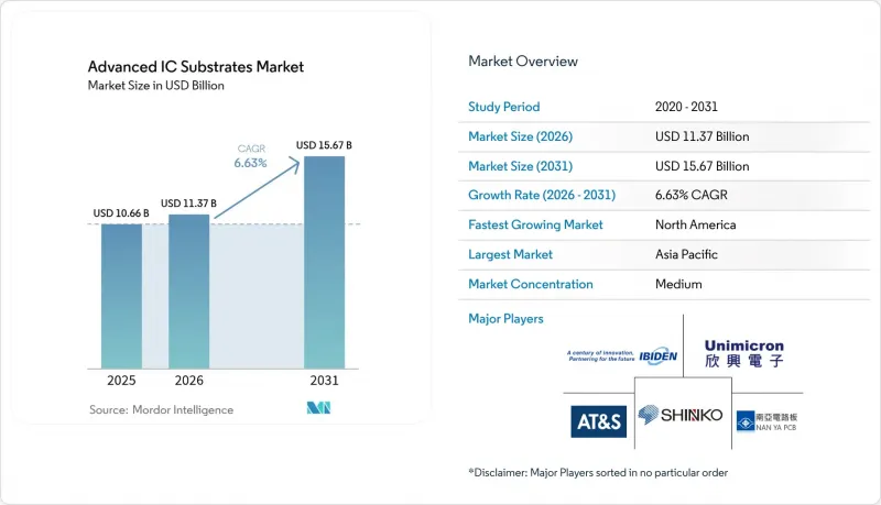
預計最先進的積體電路基板市場規模將從 2025 年的 106.6 億美元成長到 2026 年的 113.7 億美元,然後從 2026 年到 2031 年以 6.63% 的複合年成長率成長,到 2031 年達到 156.7 億美元。
本報告按基板類型(覆晶球柵陣列、覆晶晶片級封裝等)、核心材料(玻璃、陶瓷等)、封裝技術(2D覆晶、SiP/模組等)、裝置節點(28nm及以上、7-5nm等)、終端應用產業(行動/消費性電子、資料中心/人工智慧/高性能運算、其他)和地區進行細分。市場預測以美元計價。
全球先進積體電路基板市場趨勢與洞察。
人工智慧和高效能運算加速器對 ABF基板的需求正在激增。
超大規模營運商在2025年部署了超過120萬台AI加速器單元。每台單元包含4到6塊覆晶BGA基板,這些板必須能夠承受超過700瓦的功耗。由於塗層生產線的擴建無法滿足需求,平均售價從2024年的65美元上漲到2025年的82美元,供應商透過從味之素薄膜公司獲得配額來擴大利潤空間。無晶圓廠半導體製造商目前正尋求對基板工廠進行聯合投資,例如AMD與Siliconware Precision Industries成立的4億美元合資企業,推出合資企業獲得了台灣一家新工廠30%的產能。這些預購協議給供應配額無法得到保障的中型供應商帶來了壓力,加劇了產能領域的寡占。只要加速器出貨量持續每兩年加倍,先進的IC基板市場就將繼續以高價吸收對ABF面板的額外需求。
小型化和異構整合趨勢
晶片組架構透過將單晶片分割成運算、I/O 和儲存單元,可將晶片面積減少高達 40%,從而實現節點混合策略。這種佈局需要小於 50微米的微孔和間距為 2微米的線路重布,這使得 ABF 和新興玻璃基片都達到了物理極限。為了保持設計訂單的競爭力, IBIDEN和 AT&S 將在流片前 18 個月派遣工程師進駐台積電封裝中心,預計到 2025 年將佔據 2.5D 中介層基板市場 40% 的佔有率。這種合作模式將使基板製造從通用生產轉向半設計服務,加快學習曲線,並進一步加深供應商鎖定。未來十年,無法使其藍圖與代工廠保持一致的供應商將面臨被淘汰到傳統節點的風險,這可能會縮小其在尖端 IC基板市場的潛在收入。
ABF基板產能短缺及前置作業時間急劇增加
2025年初,人工智慧需求超過供應18個百分點,導致14層ABF基板的前置作業時間延長至28週。中型無晶圓廠設計公司被迫支付15-20%的現貨溢價,或將流片週期推遲多達四個季度。設備供應瓶頸依然存在,LPKF Laser和三菱電機佔了雷射鑽孔產能的約70%,但卻面臨長達18個月的交貨積壓。因此,主要供應商正在超額訂購味之素薄膜,進一步加劇了小型競爭對手的供不應求。除非新的塗覆生產線在2027年前投入運作,否則先進積體電路基板市場將繼續面臨產能限制,預計其複合年成長率將下降約1.2個百分點。
細分市場分析
到2025年,覆晶BGA將佔據最先進的IC基板市場43.89%的市場佔有率,這反映了其在行動應用處理器和伺服器CPU領域的穩固地位。在智慧型手錶、擴增實境(AR)頭戴裝置和採用可彎曲聚醯亞胺芯的醫療貼片等產品的推動下,軟硬複合和軟性CSP封裝形式將以7.71%的複合年成長率成長至2031年。到2025年,覆晶CSP將佔超薄智慧型手機出貨量的22%,而有機BGA和LGA封裝將在對成本高度敏感的汽車控制器市場保持18%的穩定佔有率。剩餘的16%市場佔有率將由其他封裝形式構成,包括嵌入式晶片和無芯基板,這主要得益於5G毫米波前端模組的需求,這些模組需要更佳的導熱路徑。
由於多腔佈局和精細線路重布,採用晶片級封裝的覆晶BGA製程增加了製造複雜性,導致平均售價(ASP)上漲25-35%。採用雷射直接光刻(LDI)和改良型半添加劑處理的供應商已佔據這一高利潤細分市場約70%的佔有率,重塑了競爭格局。相較之下,面板級加工提高了軟硬複合的良率,但到2025年,平均售價將下降5%,迫使專業製造商調整其營運模式。因此,就技術組合而言,儘管軟式電路板的銷量顯著成長,但盈利仍然偏向先進的覆晶封裝,整個尖端積體電路基板市場的產品策略仍處於微妙的平衡狀態。
味之素的積層製造薄膜在2025年佔總銷售額的52.78%,鞏固了其作為智慧型手機、PC和伺服器旗艦產品的地位。受4奈米以下邏輯電路和共封裝光學元件中對超低翹曲和光佈線的需求驅動,玻璃基板預計到2031年將以7.47%的複合年成長率成長。雙馬來亞醯胺三嗪佔高溫汽車模組出貨量的15%,而用於射頻功率和LED構裝的陶瓷則保持在9%。正在研發中的混合玻璃-有機層壓板兼具成本效益和玻璃般的平整度,預計在2027年後挑戰純積層製造薄膜的地位。
超大規模資料中心業者營運商對康寧和AGC試點生產線的資助,預計在2031年將玻璃在高階伺服器插槽中的佔有率提升至15-20%,並可能帶來與先進積體電路基板市場規模相當的新收入。汽車產業每年2-3%的價格下調壓力迫使BT和陶瓷供應商實現檢測和測試的自動化,以保障利潤率。因此,長期的材料策略取決於如何在不同的終端應用領域中平衡ABF(先進基板)的產量、玻璃性能和BT的成本控制。
區域分析
到2025年,亞太地區將佔據先進IC基板市場78.36%的佔有率。這主要得益於台灣地區4.2億片覆晶BGA的出貨量以及日本在14層和16層伺服器基板的專業化發展。韓國廠商透過轉向面板加工,將其軟硬複合基板的產量擴大到8500萬片,實現了與條狀基板成本持平。中國廠商透過擴大傳統製程節點的產能,並將價格定得比台灣平均價格低10-15%,將其在汽車和工業領域的市佔率提升至18%。印度仍是新興市場參與者,由於良率挑戰,塔塔電子和凱因斯科技的試點生產線出貨量不足500萬基板。
預計到2031年,北美市場將以7.69%的複合年成長率成長,這主要得益於《晶片和封裝技術法案》(CHIPS Act)提供的28億美元獎勵,該措施旨在扶持美國本土的基板和封裝工廠。 IbidenIBIDEN位於亞利桑那州、投資12億美元的工廠以及AT&S公司位於德克薩斯、投資8億美元的工廠預計將從2027年起合計每月生產5萬塊面板,為美國無廠半導體公司提供第二個生產基地。隨著Tripod Technology和Zhen Ding Technology在墨西哥瓜達拉哈拉擴大業務,為汽車和工業客戶提供服務,近岸外包已使墨西哥的產能在2025年增加2,200萬塊。美國合約中的雙重採購條款已經導致訂單多元化,迫使現有的亞洲公司設立北美子公司以保護其市場佔有率。
到2025年,歐洲將佔總銷售額的6%,其中大部分集中在奧地利和德國,AT&S和Schweizer Electronic在這兩個國家為汽車和工業客戶提供服務。 AT&S位於萊奧本的工廠擴建項目獲得了歐盟「晶片基金」5億歐元的資助,預計從2027年起每月將新增2萬塊FC-BGA面板的產能。南美洲和中東/非洲合計佔比不到2%,反映出半導體組裝能有限以及待開發區建廠投資回收期較長。除非推出補貼機制來抵消高昂的資本成本,否則這些地區在尖端積體電路基板市場中仍將處於邊緣地位。
其他好處:
- Excel格式的市場預測(ME)表
- 3個月的分析師支持
目錄
第1章:引言
- 研究假設和市場定義
- 調查範圍
第2章:調查方法
第3章執行摘要
第4章 市場狀況
- 市場概覽
- 市場促進因素
- 人工智慧和高效能運算加速器對 ABF基板的需求正在激增。
- 小型化和異構整合趨勢
- 5G 的部署正在推動高頻射頻封裝技術的發展。
- 採用需要超低損耗基板的共封裝光學元件。
- 與基板製造相關的CHIPS方法在地化補貼
- 大螢幕有機基板生產線正在降低每個晶片的成本。
- 市場限制因素
- ABF基板供不應求和前置作業時間急劇增加
- 高資本密集度與流程複雜性
- 對單一來源ABF積膜的依賴性
- 加強對含氟溶劑的排放法規
- 產業價值鏈分析
- 監理情勢
- 技術展望
- 波特五力分析
- 價格分析
- 宏觀經濟因素的影響
第5章 市場規模與成長預測
- 依基材類型
- 覆晶球柵陣列
- 覆晶和晶片級封裝
- 有機球柵陣列/平面網格陣列
- 軟硬複合和軟性晶片級封裝
- 其他基質類型
- 主要材料
- 味之素增效膜
- 雙馬來亞醯胺三嗪樹脂
- 玻璃
- 陶瓷製品
- 產品技術
- 2D覆晶
- 2.5D 中介層
- 3D-IC/SoIC
- 扇出 WLP
- SiP/模組
- 按設備節點
- 28奈米或更大
- 16/14~10 nm
- 7~5 nm
- 4奈米或更小
- 按最終用途行業分類
- 行動和消費者
- 汽車和運輸業
- 資訊科技和通訊基礎設施
- 資料中心/人工智慧和高效能運算
- 其他終端用戶產業
- 按地區
- 北美洲
- 美國
- 加拿大
- 墨西哥
- 南美洲
- 巴西
- 阿根廷
- 其他南美國家
- 歐洲
- 英國
- 德國
- 法國
- 義大利
- 其他歐洲國家
- 亞太地區
- 中國
- 日本
- 印度
- 韓國
- 其他亞太國家
- 中東和非洲
- 中東
- 阿拉伯聯合大公國
- 沙烏地阿拉伯
- 其他中東國家
- 非洲
- 南非
- 埃及
- 其他非洲國家
- 中東
- 北美洲
第6章 競爭情勢
- 市場集中度
- 策略趨勢
- 市佔率分析
- 公司簡介
- Unimicron Technology Corp.
- Ibiden Co., Ltd.
- Nan Ya Printed Circuit Board Corp.
- Shinko Electric Industries Co., Ltd.
- AT&S Austria Technologie & Systemtechnik AG
- Kinsus Interconnect Technology Corp.
- Samsung Electro-Mechanics Co., Ltd.
- Kyocera Corporation
- ASE Technology Holding Co., Ltd.
- LG Innotek Co., Ltd.
- Simmtech Co., Ltd.
- TTM Technologies, Inc.
- Fujitsu Interconnect Technologies Ltd.
- JCET Group Co., Ltd.
- Panasonic Holdings Corporation
- Zhen Ding Technology Holding Ltd.
- Shennan Circuits Co., Ltd.
- Daeduck Electronics Co., Ltd.
- WUS Printed Circuit Co., Ltd.
- Zhejiang Kingdom Sci-Tech Co., Ltd.
- SKC Absolics Inc.
- Tripod Technology Corp.
- Toppan Inc.
第7章 市場機會與未來展望
According to Mordor Intelligence, the advanced IC substrates market size is expected to grow from USD 10.66 billion in 2025 to USD 11.37 billion in 2026 and is forecast to reach USD 15.67 billion by 2031 at a 6.63% CAGR over 2026-2031.
This report is Segmented by Substrate Type (Flip-Chip Ball Grid Array, Flip-Chip Chip Scale Package, and More), Core Material (Glass, Ceramic, and More), Packaging Technology (2D Flip-Chip, SiP/Module, and More), Device Node (Above 28nm, 7-5nm, and More), End-Use Industry (Mobile and Consumer, Data-Centre/AI and HPC, and More), and Geography. The Market Forecasts are Provided in Terms of Value (USD).
Global Advanced IC Substrates Market Trends and Insights
Surge in ABF-Substrate Demand for AI and HPC Accelerators
Hyperscale operators installed more than 1.2 million AI accelerator units in 2025, each integrating four to six flip-chip BGA substrates that must withstand power draw above 700 watts. Average selling prices climbed from USD 65 in 2024 to USD 82 in 2025 as coating-line additions lagged demand, widening suppliers' margins as they locked in Ajinomoto film allocations. Fabless chipmakers are now co-investing in substrate plants, illustrated by AMD's USD 400 million venture with Siliconware Precision Industries that secures 30% of a new Taiwanese facility's output. These forward-buy agreements squeeze mid-tier vendors that lack guaranteed slots, reinforcing a capacity oligopoly. As long as accelerator shipments double every 2 years, the advanced IC substrates market will continue to absorb incremental ABF panels at premium pricing.
Miniaturisation and Heterogeneous Integration Trend
Chiplet architectures slice monolithic dies into smaller compute, I/O, and memory tiles, cutting die area by up to 40% and enabling node-mixing strategies. Such layouts demand microvias below 50 micrometers and redistribution layers at 2 micrometer pitch, pushing both ABF and emerging glass cores to their physical limits. To stay design-win-relevant, Ibiden and AT&S embedded engineers at TSMC's packaging center 18 months ahead of tape-out, capturing 40% of the 2.5D interposer substrate pool by 2025. The collaboration model shifts substrate manufacturing from commodity production toward quasi-design services, accelerating learning curves and deepening vendor lock-in. Over the next decade, suppliers unable to align roadmaps with foundries risk relegation to legacy nodes, curtailing addressable revenue in the advanced IC substrates market.
ABF-Substrate Capacity Shortage and Lead-Time Spikes
Lead times for 14-layer ABF substrates stretched to 28 weeks in early 2025 as AI demand outran supply by 18 percentage points. Mid-tier fabless designers either paid spot premiums of 15-20% or postponed tape-outs by up to three quarters. Equipment chokepoints persist: LPKF Laser and Mitsubishi Electric hold roughly 70% of laser-drill capacity and face an 18-month delivery backlog. Large suppliers, therefore, over-book Ajinomoto film, amplifying scarcity for smaller rivals. Unless new coating lines come online before 2027, the advanced IC substrates market will remain capacity-constrained, trimming potential CAGR by an estimated 1.2 percentage points.
Other drivers and restraints analyzed in the detailed report include:
- 5G Roll-Out Boosting High-Frequency RF Packaging
- Co-Packaged Optics Adoption Requiring Ultra-Low-Loss Substrates
- High Capital Intensity and Process Complexity
For complete list of drivers and restraints, kindly check the Table Of Contents.
Segment Analysis
Flip-chip BGA commanded 43.89% of the advanced IC substrates market share in 2025, reflecting its entrenched position in mobile application processors and server CPUs. Rigid-flex and flexible CSP formats are advancing at a 7.71% CAGR through 2031, driven by smartwatches, augmented-reality headsets, and medical patches that benefit from bendable polyimide cores. Flip-chip CSP held 22% of 2025 shipment volume for ultra-thin smartphones, while organic BGA and LGA accounted for a steady 18% of volume in cost-focused automotive controllers. Other formats, including embedded-die and coreless substrates, accounted for the remaining 16%, driven by 5G millimeter-wave front-end modules that require improved thermal paths.
Chiplet-ready flip-chip BGA variants command 25-35% ASP premiums because multi-cavity layouts and fine redistribution layers raise manufacturing complexity. Suppliers with laser-direct-imaging and modified semi-additive processes secured roughly 70% of this high-margin pool, reshaping competitive balance. By contrast, panel-level processing helped rigid-flex yields, but the resulting 5% ASP erosion in 2025 pressured specialists to consolidate. The technology mix, therefore, tilts profitability toward advanced flip-chip formats even as unit growth skews toward flexible substrates, keeping product strategy nuanced across the advanced IC substrates market.
Ajinomoto build-up film captured 52.78% of 2025 revenue, reinforcing its status as the incumbent core for smartphones, PCs, and servers. Glass substrates are set for a 7.47% CAGR through 2031 as sub-4-nanometer logic and co-packaged optics demand ultra-low warpage and optical routing. Bismaleimide-triazine accounted for 15% of the volume in high-temperature automotive modules, while ceramic remained at 9% for RF power and LED packages. Hybrid glass-organic laminates under development could combine cost efficiency with glass-level flatness, challenging pure ABF beyond 2027.
Hyperscaler funding for Corning and AGC pilot lines may lift glass to 15-20% of premium server sockets by 2031, injecting fresh revenue into the advanced IC substrates market size. Automotive price-down pressure of 2-3% a year forces BT and ceramic vendors to automate inspection and test to protect margins. As a result, the long-term material strategy hinges on balancing ABF volume, glass performance, and BT cost discipline across diversified end uses.
Complete Report Scope:
- By Substrate Type
- Flip-Chip Ball Grid Array
- Flip-Chip Chip Scale Package
- Organic Ball Grid Array / Land Grid Array
- Rigid-Flex and Flexible Chip Scale Package
- Other Substrate Types
- By Core Material
- Ajinomoto Build-up Film
- Bismaleimide-Triazine Resin
- Glass
- Ceramic
- By Packaging Technology
- 2D Flip-Chip
- 2.5D Interposer
- 3D-IC / SoIC
- Fan-Out WLP
- SiP / Module
- By Device Node
- Above 28 nm
- 16/14-10 nm
- 7-5 nm
- 4 nm and below
- By End-Use Industry
- Mobile and Consumer
- Automotive and Transportation
- IT and Telecom Infrastructure
- Data-Centre / AI and HPC
- Other End-Use Industries
- By Geography
- North America
- United States
- Canada
- Mexico
- South America
- Brazil
- Argentina
- Rest of South America
- Europe
- United Kingdom
- Germany
- France
- Italy
- Rest of Europe
- Asia Pacific
- China
- Japan
- India
- South Korea
- Rest of Asia Pacific
- Middle East and Africa
- Middle East
- United Arab Emirates
- Saudi Arabia
- Rest of Middle East
- Africa
- South Africa
- Egypt
- Rest of Africa
- Middle East
- North America
Geography Analysis
Asia-Pacific accounted for 78.36% of the advanced IC substrates market size in 2025, anchored by Taiwan's 420 million flip-chip BGA shipments and Japan's specialization in 14-layer and 16-layer server substrates. South Korean vendors raised rigid-flex output to 85 million units and achieved cost parity with strip formats by switching to panel processing. Chinese suppliers increased legacy-node capacity and priced 10-15% below Taiwanese averages, boosting their share of automotive and industrial demand to 18%. India remained a nascent player, as pilot lines at Tata Electronics and Kaynes Technology shipped fewer than 5 million substrates due to yield challenges.
North America is projected to expand at a 7.69% CAGR through 2031, propelled by USD 2.8 billion in CHIPS Act incentives tied to domestic substrate and packaging plants. Ibiden's USD 1.2 billion Arizona fab and AT&S's USD 800 million Texas facility will together add 50,000 panels per month after 2027, giving U.S. fabless firms a second sourcing hub. Mexican near-shoring added 22 million units in 2025 as Tripod Technology and Zhen Ding Technology enlarged Guadalajara operations to serve automotive and industrial customers. Dual-sourcing clauses in U.S. contracts are already fragmenting order volumes, pressuring Asian incumbents to establish North American subsidiaries to defend their share.
Europe accounted for 6% of 2025 revenue, concentrated in Austria and Germany, where AT&S and Schweizer Electronic cater to automotive and industrial clients. AT&S's Leoben expansion, backed by EUR 500 million in EU Chips funds, will bring 20,000 additional FC-BGA panels per month starting in 2027. South America, the Middle East, and Africa together accounted for less than 2%, reflecting limited semiconductor assembly capacity and long payback periods for greenfield fabs. Unless subsidy frameworks emerge to offset high capital costs, these regions will remain fringe participants in the advanced IC substrates market.
- Unimicron Technology Corp.
- Ibiden Co., Ltd.
- Nan Ya Printed Circuit Board Corp.
- Shinko Electric Industries Co., Ltd.
- AT&S Austria Technologie & Systemtechnik AG
- Kinsus Interconnect Technology Corp.
- Samsung Electro-Mechanics Co., Ltd.
- Kyocera Corporation
- ASE Technology Holding Co., Ltd.
- LG Innotek Co., Ltd.
- Simmtech Co., Ltd.
- TTM Technologies, Inc.
- Fujitsu Interconnect Technologies Ltd.
- JCET Group Co., Ltd.
- Panasonic Holdings Corporation
- Zhen Ding Technology Holding Ltd.
- Shennan Circuits Co., Ltd.
- Daeduck Electronics Co., Ltd.
- WUS Printed Circuit Co., Ltd.
- Zhejiang Kingdom Sci-Tech Co., Ltd.
- SKC Absolics Inc.
- Tripod Technology Corp.
- Toppan Inc.
Additional Benefits:
- The market estimate (ME) sheet in Excel format
- 3 months of analyst support
TABLE OF CONTENTS
1 INTRODUCTION
- 1.1 Study Assumptions and Market Definition
- 1.2 Scope of the Study
2 RESEARCH METHODOLOGY
3 EXECUTIVE SUMMARY
4 MARKET LANDSCAPE
- 4.1 Market Overview
- 4.2 Market Drivers
- 4.2.1 Surge in ABF-Substrate Demand for AI and HPC Accelerators
- 4.2.2 Miniaturisation and Heterogeneous Integration Trend
- 4.2.3 5G Roll-Out Boosting High-Frequency RF Packaging
- 4.2.4 Co-Packaged Optics Adoption Requiring Ultra-Low-Loss Substrates
- 4.2.5 CHIPS-Style Localisation Subsidies Tied to Substrate Fabs
- 4.2.6 Large-Panel Organic Substrate Lines Lowering Cost Per Die
- 4.3 Market Restraints
- 4.3.1 ABF-Substrate Capacity Shortage and Lead-Time Spikes
- 4.3.2 High Capital Intensity and Process Complexity
- 4.3.3 Single-Source Dependency on ABF Build-Up Films
- 4.3.4 Stricter Fluorinated-Solvent Emission Regulations
- 4.4 Industry Value Chain Analysis
- 4.5 Regulatory Landscape
- 4.6 Technological Outlook
- 4.7 Porter's Five Forces Analysis
- 4.7.1 Bargaining Power of Suppliers
- 4.7.1.1 Bargaining Power of Consumers
- 4.7.1.2 Threat of New Entrants
- 4.7.1.3 Threat of Substitutes
- 4.7.1.4 Intensity of Competitive Rivalry
- 4.7.1 Bargaining Power of Suppliers
- 4.8 Pricing Analysis
- 4.9 Impact of Macroeconomic Factors
5 MARKET SIZE AND GROWTH FORECASTS (VALUE)
- 5.1 By Substrate Type
- 5.1.1 Flip-Chip Ball Grid Array
- 5.1.2 Flip-Chip Chip Scale Package
- 5.1.3 Organic Ball Grid Array / Land Grid Array
- 5.1.4 Rigid-Flex and Flexible Chip Scale Package
- 5.1.5 Other Substrate Types
- 5.2 By Core Material
- 5.2.1 Ajinomoto Build-up Film
- 5.2.2 Bismaleimide-Triazine Resin
- 5.2.3 Glass
- 5.2.4 Ceramic
- 5.3 By Packaging Technology
- 5.3.1 2D Flip-Chip
- 5.3.2 2.5D Interposer
- 5.3.3 3D-IC / SoIC
- 5.3.4 Fan-Out WLP
- 5.3.5 SiP / Module
- 5.4 By Device Node
- 5.4.1 Above 28 nm
- 5.4.2 16/14-10 nm
- 5.4.3 7-5 nm
- 5.4.4 4 nm and below
- 5.5 By End-Use Industry
- 5.5.1 Mobile and Consumer
- 5.5.2 Automotive and Transportation
- 5.5.3 IT and Telecom Infrastructure
- 5.5.4 Data-Centre / AI and HPC
- 5.5.5 Other End-Use Industries
- 5.6 By Geography
- 5.6.1 North America
- 5.6.1.1 United States
- 5.6.1.2 Canada
- 5.6.1.3 Mexico
- 5.6.2 South America
- 5.6.2.1 Brazil
- 5.6.2.2 Argentina
- 5.6.2.3 Rest of South America
- 5.6.3 Europe
- 5.6.3.1 United Kingdom
- 5.6.3.2 Germany
- 5.6.3.3 France
- 5.6.3.4 Italy
- 5.6.3.5 Rest of Europe
- 5.6.4 Asia Pacific
- 5.6.4.1 China
- 5.6.4.2 Japan
- 5.6.4.3 India
- 5.6.4.4 South Korea
- 5.6.4.5 Rest of Asia Pacific
- 5.6.5 Middle East and Africa
- 5.6.5.1 Middle East
- 5.6.5.1.1 United Arab Emirates
- 5.6.5.1.2 Saudi Arabia
- 5.6.5.1.3 Rest of Middle East
- 5.6.5.2 Africa
- 5.6.5.2.1 South Africa
- 5.6.5.2.2 Egypt
- 5.6.5.2.3 Rest of Africa
- 5.6.5.1 Middle East
- 5.6.1 North America
6 COMPETITIVE LANDSCAPE
- 6.1 Market Concentration
- 6.2 Strategic Moves
- 6.3 Market Share Analysis
- 6.4 Company Profiles (includes Global Level Overview, Market Level Overview, Core Segments, Financials as available, Strategic Information, Market Rank/Share, Products and Services, Recent Developments)
- 6.4.1 Unimicron Technology Corp.
- 6.4.2 Ibiden Co., Ltd.
- 6.4.3 Nan Ya Printed Circuit Board Corp.
- 6.4.4 Shinko Electric Industries Co., Ltd.
- 6.4.5 AT&S Austria Technologie & Systemtechnik AG
- 6.4.6 Kinsus Interconnect Technology Corp.
- 6.4.7 Samsung Electro-Mechanics Co., Ltd.
- 6.4.8 Kyocera Corporation
- 6.4.9 ASE Technology Holding Co., Ltd.
- 6.4.10 LG Innotek Co., Ltd.
- 6.4.11 Simmtech Co., Ltd.
- 6.4.12 TTM Technologies, Inc.
- 6.4.13 Fujitsu Interconnect Technologies Ltd.
- 6.4.14 JCET Group Co., Ltd.
- 6.4.15 Panasonic Holdings Corporation
- 6.4.16 Zhen Ding Technology Holding Ltd.
- 6.4.17 Shennan Circuits Co., Ltd.
- 6.4.18 Daeduck Electronics Co., Ltd.
- 6.4.19 WUS Printed Circuit Co., Ltd.
- 6.4.20 Zhejiang Kingdom Sci-Tech Co., Ltd.
- 6.4.21 SKC Absolics Inc.
- 6.4.22 Tripod Technology Corp.
- 6.4.23 Toppan Inc.
7 MARKET OPPORTUNITIES AND FUTURE OUTLOOK
- 7.1 White-Space and Unmet-Need Assessment

 全球先進積體電路基板市場(2027-2037 年)
 先進積體電路基板市場-2026-2032年全球市場預測
 先進封裝基板市場分析與預測(至2035年):按類型、產品、技術、應用、材料類型、製程、最終用戶、功能和設備分類
 先進積體電路基板市場規模、佔有率、趨勢和預測:按類型、應用和地區分類,2026-2034年
 先進積體電路基板市場規模、佔有率和成長分析:按類型、技術、應用、材料、終端用戶產業和地區分類-2026-2033年產業預測
 半導體先進基板市場預測至2034年:按產品類型、技術、應用、最終用戶、分銷管道和地區分類的全球分析
 全球先進積體電路基板市場規模、佔有率、產業分析報告:按類型、技術、應用和地區分類、展望和預測,2025-2032 年
 全球先進積體基板市場
 先進積體電路載板市場(按類型、按封裝技術、按材料、按最終用途、按國家和地區)-2025 年至 2032 年全球產業分析、市場規模、市場佔有率及預測
 先進IC基板市場規模、佔有率及趨勢分析報告:按類型、技術、應用、地區及細分市場預測,2025-2033年