


 |
市場調查報告書
商品編碼
2122312
半導體晶圓拋光和研磨設備:市場佔有率分析、行業趨勢和統計數據以及成長預測(2026-2031 年)Semiconductor Wafer Polishing And Grinding Equipment - Market Share Analysis, Industry Trends & Statistics, Growth Forecasts (2026 - 2031) |
||||||

※ 本網頁內容可能與最新版本有所差異。詳細情況請與我們聯繫。
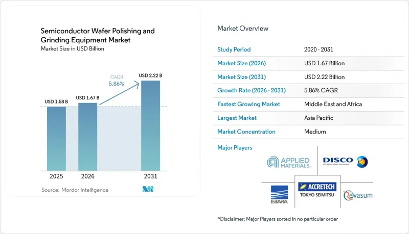
根據 Mordor Intelligence 預測,半導體晶圓拋光和研磨設備的市場規模預計將從 2025 年的 15.8 億美元成長到 2026 年的 16.7 億美元,然後從 2026 年到 2031 年以 5.86% 的複合年成長率成長,到 2031 年達到 2031 年達到 2031 億美元。
[1] 美國半導體產業協會 (SIA),「2024 年美國半導體產業狀況」。本報告按設備類型(晶圓研磨設備、其他)、晶圓尺寸(150 毫米以下、200 毫米、300 毫米、450 毫米以上)、技術(背面研磨、其他)、半導體類型(記憶體、邏輯/SoC、其他)、最終用戶(垂直整合設備製造商、其他)和地區(北美、南美、歐洲、亞太、中東和非洲)進行分類。
全球半導體晶圓拋光研磨設備市場趨勢及洞察
亞洲地區搭載先進節點晶片的消費性電子產品市場擴張
旗艦智慧型手機和人工智慧穿戴裝置在中國、印度和東南亞的迅速普及,加速了對3奈米以下裝置的需求,這些裝置需要原子級光滑的晶圓表面和十億分之一等級的缺陷密度。儘管出口許可證不確定性,但當地代工廠已擴大了化學機械拋光(CMP)和微研磨的生產能力,而設備製造商則採用了符合嚴格環保標準且不影響平整度的無氯拋光墊。隨著多核心SoC的普及,不同材料堆疊的製程均勻性變得至關重要,這推動了專用於異構層的自適應控制CMP系統的投資。
小型化趨勢的日益明顯推動了對 300 毫米和 450 毫米 CMP 設備的需求不斷成長。
為了追求成本效益高的晶片密度,300mm 晶片仍然是主流尺寸,但 450mm 晶片的研發再次引起關注,因為使用更大的基板可以將晶片面積增加 2.25 倍,從而滿足檢測需求。設備製造商一直在努力擴大晶片尺寸,他們透過強化壓板、最佳化漿料分佈以及整合原位測量功能,以在更大的表面積上保持奈米級的去除均勻性。由台積電 (TSMC) 開發的 510mm x 515mm 矩形基板原型提供了一種替代方案,可在不徹底改造傳統設備架構的情況下,將可用面積擴大三倍。
300mm設備的資本投資成本高,投資回收期長。
截至2024年,一台300毫米CMP平台的成本在300萬美元至500萬美元之間,設備升級還需要額外投入100萬美元至200萬美元,這意味著對於小批量晶圓廠而言,投資回收期超過四年。中小型製造商推遲了擴張計劃,轉而選擇翻新設備或共用產能模式,儘管擴大規模能顯著提高晶片的成本效益,但設備部署的整體速度仍然放緩。
細分市場分析
2025年,CMP設備佔銷售額的55.92%,並繼續在實現先進節點所需的0.1奈米或更低去除精度的平整度目標方面發揮核心作用。隨著晶圓廠採用無磨料漿料和人工智慧驅動的終點檢測技術來提高3奈米或更小節點的良率,半導體晶圓拋光和研磨設備市場也從中受益。整合式研磨和拋光平台減少了晶圓處理週期,降低了顆粒風險,並縮短了等待時間。
隨著客戶整合製程以釋放無塵室空間,預計到2031年,整合系統的複合年成長率將達到7.55%,超過獨立式研磨機。供應商正在整合封閉回路型溫度控制、預測性維護和耗材壽命分析等技術,以提高多品種生產的整體設備運轉率(OEE)。新興的研磨和切割設備能夠處理鑽石和其他超硬基板,從而拓展了半導體晶圓拋光和研磨設備市場,使其涵蓋了光電和量子裝置等細分領域。
預計到2025年,300mm節點將佔61.88%的市場收入,這得益於數十年的製程成熟、耗材最佳化以及折舊免稅額良好的晶圓廠資產。 CMP拋光墊紋理和研磨砂輪形狀的持續改進進一步提高了產能,鞏固了該細分市場在半導體晶圓拋光和研磨設備市場中的經濟優勢。
同時,450毫米及以上尺寸晶圓的複合年成長率最高,達到10.84%,這主要得益於探索矩形晶圓的試點生產線,預計矩形晶圓的晶片數量將增加兩倍。設備製造商正在開發能夠處理多種直徑晶圓的大型壓板、機器人搬運設備和高容量漿料供應系統的原型,為2028年開始的大規模部署做準備,屆時半導體晶圓拋光和研磨設備行業將進行大規模的投資回報率評估。
區域分析
2025年,亞太地區繼續佔全球銷售額的67.94%。這主要得益於台灣、韓國、日本和中國市場的強勁需求,這些地區由於整合設備藍圖和晶圓代工廠的擴張,設備採購依然保持強勁勢頭。台積電推出無氯拋光墊以及日本晶圓廠叢集的補貼,進一步強化了該地區對環保設備的偏好。儘管出口不確定性加劇了中國晶圓廠對本土供應商的依賴,但高階CMP設備的進口仍透過許可證豁免得以繼續,從而維持了半導體晶圓拋光和研磨設備市場的基本需求。
在北美,2022 年《晶片與科學法案》的頒布推動了投資的復甦。該法案調動了 520 億美元的獎勵,並鼓勵宣布超過 90 個建設計畫,預計到 2025 年總投資額將接近 4,500 億美元。雖然產能的提升帶動了設備訂單的成長,但預計到 2030 年將出現 6.7 萬名工程師的缺口,這使得自動化成為當務之急,因此各方都在積極尋求與學術聯盟的合作,以加快人才供給。
隨後,歐洲頒布了“TIPS法案”,這是一項耗資430億歐元(498.3億美元)的計劃,旨在到2030年佔據全球20%的市場佔有率。德國精密工程公司、法國先進封裝中心和北歐材料科學實驗室尋求配備能源回收泵和水循環迴路的CMP系統,使採購與歐盟綠色交易的目標保持一致,並促進半導體晶圓拋光和研磨設備市場差異化解決方案的發展。
其他好處
- Excel格式的市場預測(ME)表
- 3個月的分析師支持
目錄
第1章:引言
- 研究假設和市場定義
- 調查範圍
第2章:調查方法
第3章執行摘要
第4章 市場狀況
- 市場概覽
- 市場促進因素
- 亞洲地區搭載先進節點晶片的消費性電子產品市場擴張
- 小型化趨勢的日益明顯推動了對 300 毫米和 450 毫米 CMP 設備的需求不斷成長。
- 利用CHIPS方法投資美國和歐洲的晶圓代工產能
- 由於向SiC/GaN功率元件過渡,對超高精度研磨的需求日益成長。
- 提高 3D-IC 和異質整合良率的必要性。
- 永續發展需求推動了無漿拋光技術的進步
- 市場限制因素
- 300mm設備的資本投資成本高,投資回收期長。
- 耗材成本上漲(墊片、漿料、鑽石砂輪)
- 出口限制和智慧財產權壁壘限制了對中國的出口。
- 工藝配置和維護方面熟練技術人員短缺
- 價值鏈分析
- 監管和技術展望
- 波特五力模型
- 產業價值鏈分析
- 二手設備市場的市場動態
- 投資分析
- 宏觀經濟影響評估
第5章 市場規模與成長預測
- 依設備類型
- 晶圓研磨機
- 晶圓拋光(CMP)設備
- 一體式研磨拋光裝置
- 其他(包裹、切片、削薄)
- 按晶圓尺寸
- 150毫米或更小
- 200mm
- 300mm
- 450毫米或以上
- 透過技術
- 反向研磨
- 雙面研磨
- 化學機械拋光(CMP)
- 邊緣研磨和斜面拋光
- 依半導體類型
- 記憶體(DRAM、NAND)
- 邏輯SoC
- 功率模擬(Si、SiC、GaN)
- MEMS感測器
- CMOS影像感測器
- LED和光電子學
- 最終用戶
- 鑄造廠
- 垂直整合設備製造商(IDM)
- OSAT/先進包裝設施
- 研究與開發機構及試驗生產線
- 按地區
- 北美洲
- 美國
- 加拿大
- 南美洲
- 巴西
- 其他南美國家
- 歐洲
- 德國
- 英國
- 法國
- 義大利
- 其他歐洲國家
- 亞太地區
- 中國
- 台灣
- 日本
- 韓國
- 印度
- 其他亞太國家
- 中東和非洲
- 中東
- 沙烏地阿拉伯
- 阿拉伯聯合大公國
- 土耳其
- 其他中東國家
- 非洲
- 南非
- 奈及利亞
- 其他非洲地區
- 中東
- 北美洲
第6章 競爭情勢
- 市場集中度
- 策略趨勢
- 市佔率分析
- 公司簡介
- Applied Materials Inc.
- Ebara Corporation
- DISCO Corporation
- Tokyo Seimitsu Co. Ltd(ACCRETECH)
- Revasum Inc.
- Komatsu NTC Ltd.
- Okamoto Machine Tool Works Co. Ltd.
- Lapmaster Wolters GmbH(Precision Surfacing Solutions)
- Logitech Ltd.
- Entrepix Inc.(Amtech Systems)
- G&N Genauigkeits Maschinenbau Nurnberg GmbH
- Hantop Intelligence Tech Co. Ltd.
- CMP-Tec Inc.
- Koyo Machinery Co. Ltd.
- Shanghai ShinEne Technology Co. Ltd.
- Qingdao Lapping & Polishing Equipment Co. Ltd.
- Nagase Integrex Co. Ltd.
- Strausbaugh Inc.(S-Cubed)
- Pureon AG
- Vibrantz Technologies Inc.
- Axus Technology
- SHANGHAI FAMOUS TRADE CO.,LTD(ZMSH)
- Huahai Machinery Group
- Hansung Engineering Co. Ltd.
- GPMT Co. Ltd.
第7章 市場機會與未來展望
According to Mordor Intelligence, the semiconductor wafer polishing and grinding equipment market size is expected to grow from USD 1.58 billion in 2025 to USD 1.67 billion in 2026 and is forecast to reach USD 2.22 billion by 2031 at 5.86% CAGR over 2026-2031.
[1] Semiconductor Industry Association, "2024 State of the U.S. This report is Segmented by Equipment Type (Wafer Grinding Machines, and More), Wafer Size (<=150 Mm, 200 Mm, 300 Mm, and 450 Mm and Above), Technology (Back-Grinding, and More), Semiconductor Type (Memory, Logic and SoC, and More), End-User (Integrated Device Manufacturers, and More), and Geography (North America, South America, Europe, Asia-Pacific, and Middle East and Africa).
Global Semiconductor Wafer Polishing And Grinding Equipment Market Trends and Insights
Growing consumption of consumer electronics with advanced-node chips in Asia
Rapid uptake of flagship smartphones and AI-enabled wearables across China, India, and Southeast Asia accelerated demand for sub-3 nm devices that require atomically smooth wafer surfaces and defect densities measured in parts per billion. Local foundries expanded CMP and fine-grinding capacity despite export-license uncertainty, while tool makers introduced chlorine-free pads that met strict environmental codes without compromising planarity. As multi-core SoCs proliferated, process uniformity across diverse material stacks became critical, spurring investment in adaptive-control CMP systems tailored for heterogeneous layers.
Miniaturization push driving demand for 300 mm and 450 mm CMP tools
The search for cost-effective die density sustained 300 mm as the mainstream format, yet exploratory 450 mm development resurfaced because a larger blank yields 2.25 times more die area. Tool makers tackled the scale-up challenge by reinforcing platens, optimizing slurry distribution, and embedding in-situ metrology to maintain nanometer-level removal uniformity across wider surfaces. TSMC's prototype 510 mm X 515 mm rectangular substrate hinted at an alternate path that could triple usable area without fully overhauling legacy tool architectures.
High capital cost and long ROI cycle for 300 mm tools
A single 300 mm CMP platform carried a USD 3-5 million price tag in 2024, with facility upgrades adding USD 1-2 million, stretching payback beyond 4 years in lower-volume fabs. Smaller players delayed expansion and opted for refurbished or shared-capacity models, slowing overall tool uptake despite clear cost-per-die advantages at scale.
Other drivers and restraints analyzed in the detailed report include:
- Foundry capacity investments in the U.S. and Europe under the CHIPS Act
- Transition to SiC/GaN power devices requires ultra-precision grinding
- Export controls and IP barriers limiting shipments to China
For complete list of drivers and restraints, kindly check the Table Of Contents.
Segment Analysis
CMP tools generated 55.92% of 2025 revenue and remained central to advanced-node planarity targets that mandate removal accuracy below 0.1 nm. The semiconductor wafer polishing and grinding equipment market benefited as fabs adopted abrasive-free slurries and AI-assisted endpoint detection to push sub-3 nm yields upward. Integrated grinder-polisher platforms reduced wafer transfers, trimming particle risks, and cutting queue time.
Integrated systems' 7.55% CAGR through 2031 outpaced standalone grinders as customers consolidated process steps to free cleanroom space. Vendors bundled closed-loop temperature control, predictive maintenance, and consumable-life analytics, enhancing OEE for high-mix production. Emerging lapping and slicing tools addressed diamond and other ultra-hard substrates, extending the semiconductor wafer polishing and grinding equipment market reach into niche photonics and quantum-device lines.
The 300 mm node held 61.88% of 2025 market revenue, underlining decades of process maturity, optimized consumables, and well-depreciated fab assets. Continuous enhancements in CMP pad texture and back-grinding wheel geometry further raised throughput, reinforcing the segment's economic moat within the semiconductor wafer polishing and grinding equipment market.
Conversely, the 450 mm and above category registered the fastest 10.84% CAGR, driven by pilot lines exploring rectangular formats that promise 3X more die per wafer. Equipment makers prototyped enlarged platens, robotic handlers, and high-capacity slurry-delivery systems adaptable to multiple diameters, positioning themselves for potential mass adoption beyond 2028 as the semiconductor wafer polishing and grinding equipment industry evaluates ROI at scale.
Complete Report Scope:
- By Equipment Type
- Wafer Grinding Machines
- Wafer Polishing (CMP) Equipment
- Integrated Grinder-Polisher Tools
- Others (Lapping, Slicing Thinners)
- By Wafer Size
- <=150 mm
- 200 mm
- 300 mm
- 450 mm and Above
- By Technology
- Back-Grinding
- Double-Side Grinding
- Chemical Mechanical Polishing (CMP)
- Edge-Grinding / Bevel Polishing
- By Semiconductor Type
- Memory (DRAM, NAND)
- Logic and SoC
- Power and Analog (Si, SiC, GaN)
- MEMS and Sensors
- CMOS Image Sensors
- LED and Optoelectronics
- By End-User
- Foundries
- Integrated Device Manufacturers (IDMs)
- OSAT / Advanced Packaging Facilities
- Research and Development Institutes and Pilot Lines
- By Geography
- North America
- United States
- Canada
- South America
- Brazil
- Rest of South America
- Europe
- Germany
- United Kingdom
- France
- Italy
- Rest of Europe
- Asia-Pacific
- China
- Taiwan
- Japan
- South Korea
- India
- Rest of Asia-Pacific
- Middle East and Africa
- Middle East
- Saudi Arabia
- United Arab Emirates
- Turkey
- Rest of Middle East
- Africa
- South Africa
- Nigeria
- Rest of Africa
- Middle East
- North America
Geography Analysis
Asia-Pacific retained 67.94% of global revenue in 2025, anchored by Taiwan, South Korea, Japan, and China, where integrated device roadmaps and foundry expansions sustained tool procurements. TSMC's chlorine-free pad rollout and Japan's subsidy-backed fab clusters reinforced a regional preference for environmentally optimized equipment. Export-control uncertainties nudged Chinese fabs to local suppliers, yet high-end CMP imports persisted via license exceptions, preserving baseline semiconductor wafer polishing and grinding equipment market demand.
North America experienced an investment renaissance following the 2022 CHIPS and Science Act, which mobilized USD 52 billion in incentives and prompted over 90 fab announcements worth nearly USD 450 billion through 2025. Capacity additions raised tool orders, although technician gaps of 67,000 positions by 2030 drove automation priorities and partnerships with academic consortia to accelerate workforce pipelines.
Europe followed with the EUR 43 billion (USD 49.83 billion) Chips Act that targeted a 20% global output share by 2030. Germany's precision-engineering firms, France's advanced-packaging hubs, and Nordic material-science institutes demanded CMP systems featuring energy-recovery pumps and water-recycling loops, aligning procurement with EU Green Deal objectives and fostering differentiated semiconductor wafer polishing and grinding equipment market solutions.
- Applied Materials Inc.
- Ebara Corporation
- DISCO Corporation
- Tokyo Seimitsu Co. Ltd (ACCRETECH)
- Revasum Inc.
- Komatsu NTC Ltd.
- Okamoto Machine Tool Works Co. Ltd.
- Lapmaster Wolters GmbH (Precision Surfacing Solutions)
- Logitech Ltd.
- Entrepix Inc. (Amtech Systems)
- G&N Genauigkeits Maschinenbau Nurnberg GmbH
- Hantop Intelligence Tech Co. Ltd.
- CMP-Tec Inc.
- Koyo Machinery Co. Ltd.
- Shanghai ShinEne Technology Co. Ltd.
- Qingdao Lapping & Polishing Equipment Co. Ltd.
- Nagase Integrex Co. Ltd.
- Strausbaugh Inc. (S-Cubed)
- Pureon AG
- Vibrantz Technologies Inc.
- Axus Technology
- SHANGHAI FAMOUS TRADE CO.,LTD (ZMSH)
- Huahai Machinery Group
- Hansung Engineering Co. Ltd.
- GPMT Co. Ltd.
Additional Benefits:
- The market estimate (ME) sheet in Excel format
- 3 months of analyst support
TABLE OF CONTENTS
1 INTRODUCTION
- 1.1 Study Assumptions and Market Definition
- 1.2 Scope of the Study
2 RESEARCH METHODOLOGY
3 EXECUTIVE SUMMARY
4 MARKET LANDSCAPE
- 4.1 Market Overview
- 4.2 Market Drivers
- 4.2.1 Growing Consumption of Consumer Electronics with Advanced-Node Chips in Asia
- 4.2.2 Miniaturization Push Driving Demand for 300 mm and 450 mm CMP Tools
- 4.2.3 Foundry Capacity Investments in U.S. and Europe under CHIPS Acts
- 4.2.4 Transition to SiC/GaN Power Devices Requiring Ultra-Precision Grinding
- 4.2.5 Yield-Enhancement Needs for 3D-IC and Heterogeneous Integration
- 4.2.6 Sustainability Mandates Advancing Slurry-Free Polishing Technologies
- 4.3 Market Restraints
- 4.3.1 High Capital Cost and Long ROI Cycle for 300 mm Tools
- 4.3.2 Consumables Cost Inflation (Pads, Slurries, Diamond Wheels)
- 4.3.3 Export-Control and IP Barriers Limiting Shipments to China
- 4.3.4 Skilled-Technician Shortage for Process Set-up and Maintenance
- 4.4 Value Chain Analysis
- 4.5 Regulatory or Technological Outlook
- 4.6 Porter's Five Forces
- 4.6.1 Threat of New Entrants
- 4.6.2 Bargaining Power of Buyers
- 4.6.3 Bargaining Power of Suppliers
- 4.6.4 Threat of Substitute Products
- 4.6.5 Intensity of Competitive Rivalry
- 4.7 Industry Value Chain Analysis
- 4.8 Secondary Equipment Market Dynamics
- 4.9 Investment Analysis
- 4.10 Macroeconomic Impact Assessment
5 MARKET SIZE AND GROWTH FORECASTS (VALUE)
- 5.1 By Equipment Type
- 5.1.1 Wafer Grinding Machines
- 5.1.2 Wafer Polishing (CMP) Equipment
- 5.1.3 Integrated Grinder-Polisher Tools
- 5.1.4 Others (Lapping, Slicing Thinners)
- 5.2 By Wafer Size
- 5.2.1 <=150 mm
- 5.2.2 200 mm
- 5.2.3 300 mm
- 5.2.4 450 mm and Above
- 5.3 By Technology
- 5.3.1 Back-Grinding
- 5.3.2 Double-Side Grinding
- 5.3.3 Chemical Mechanical Polishing (CMP)
- 5.3.4 Edge-Grinding / Bevel Polishing
- 5.4 By Semiconductor Type
- 5.4.1 Memory (DRAM, NAND)
- 5.4.2 Logic and SoC
- 5.4.3 Power and Analog (Si, SiC, GaN)
- 5.4.4 MEMS and Sensors
- 5.4.5 CMOS Image Sensors
- 5.4.6 LED and Optoelectronics
- 5.5 By End-User
- 5.5.1 Foundries
- 5.5.2 Integrated Device Manufacturers (IDMs)
- 5.5.3 OSAT / Advanced Packaging Facilities
- 5.5.4 Research and Development Institutes and Pilot Lines
- 5.6 By Geography
- 5.6.1 North America
- 5.6.1.1 United States
- 5.6.1.2 Canada
- 5.6.2 South America
- 5.6.2.1 Brazil
- 5.6.2.2 Rest of South America
- 5.6.3 Europe
- 5.6.3.1 Germany
- 5.6.3.2 United Kingdom
- 5.6.3.3 France
- 5.6.3.4 Italy
- 5.6.3.5 Rest of Europe
- 5.6.4 Asia-Pacific
- 5.6.4.1 China
- 5.6.4.2 Taiwan
- 5.6.4.3 Japan
- 5.6.4.4 South Korea
- 5.6.4.5 India
- 5.6.4.6 Rest of Asia-Pacific
- 5.6.5 Middle East and Africa
- 5.6.5.1 Middle East
- 5.6.5.1.1 Saudi Arabia
- 5.6.5.1.2 United Arab Emirates
- 5.6.5.1.3 Turkey
- 5.6.5.1.4 Rest of Middle East
- 5.6.5.2 Africa
- 5.6.5.2.1 South Africa
- 5.6.5.2.2 Nigeria
- 5.6.5.2.3 Rest of Africa
- 5.6.5.1 Middle East
- 5.6.1 North America
6 COMPETITIVE LANDSCAPE
- 6.1 Market Concentration
- 6.2 Strategic Moves
- 6.3 Market Share Analysis
- 6.4 Company Profiles (includes Global-level Overview, Market-level Overview, Core Segments, Financials, Strategic Information, Market Rank/Share, Products and Services, Recent Developments)
- 6.4.1 Applied Materials Inc.
- 6.4.2 Ebara Corporation
- 6.4.3 DISCO Corporation
- 6.4.4 Tokyo Seimitsu Co. Ltd (ACCRETECH)
- 6.4.5 Revasum Inc.
- 6.4.6 Komatsu NTC Ltd.
- 6.4.7 Okamoto Machine Tool Works Co. Ltd.
- 6.4.8 Lapmaster Wolters GmbH (Precision Surfacing Solutions)
- 6.4.9 Logitech Ltd.
- 6.4.10 Entrepix Inc. (Amtech Systems)
- 6.4.11 G&N Genauigkeits Maschinenbau Nurnberg GmbH
- 6.4.12 Hantop Intelligence Tech Co. Ltd.
- 6.4.13 CMP-Tec Inc.
- 6.4.14 Koyo Machinery Co. Ltd.
- 6.4.15 Shanghai ShinEne Technology Co. Ltd.
- 6.4.16 Qingdao Lapping & Polishing Equipment Co. Ltd.
- 6.4.17 Nagase Integrex Co. Ltd.
- 6.4.18 Strausbaugh Inc. (S-Cubed)
- 6.4.19 Pureon AG
- 6.4.20 Vibrantz Technologies Inc.
- 6.4.21 Axus Technology
- 6.4.22 SHANGHAI FAMOUS TRADE CO.,LTD (ZMSH)
- 6.4.23 Huahai Machinery Group
- 6.4.24 Hansung Engineering Co. Ltd.
- 6.4.25 GPMT Co. Ltd.
7 MARKET OPPORTUNITIES AND FUTURE OUTLOOK
- 7.1 White-space and Unmet-Need Assessment

 2026年全球半導體晶圓拋光研磨設備市場報告
 半導體晶圓拋光和研磨設備市場分析:按類型、最終用戶和地區分類(2026-2034 年)
 半導體CMP拋光墊市場按類型、材質、應用和最終用戶分類 - 全球預測(2026-2032年)
 半導體拋光墊市場-2026-2031年預測晶圓研磨市場依材料、結合劑類型、砂輪幾何形狀、粒度、最終用途產業和銷售管道,全球預測,2026-2032年
 全球半導體拋光墊片市場全球半導體晶圓拋光研磨設備市場
 半導體晶圓拋光和研磨設備市場規模、佔有率、趨勢分析報告:按產品、晶圓尺寸、最終用途、地區和細分市場進行預測,2025 年至 2030 年