


 |
市場調查報告書
商品編碼
2119206
美國半導體製造設備:市場佔有率分析、行業趨勢和統計數據、成長預測(2026-2031 年)United States Semiconductor Manufacturing Equipment - Market Share Analysis, Industry Trends & Statistics, Growth Forecasts (2026 - 2031) |
||||||

※ 本網頁內容可能與最新版本有所差異。詳細情況請與我們聯繫。
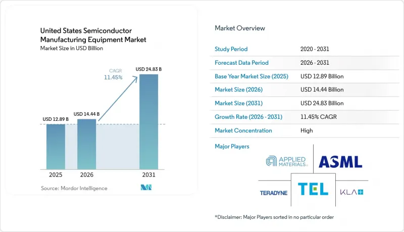
根據 Mordor Intelligence 預測,美國半導體製造設備市場規模預計在 2025 年達到 128.9 億美元,2026 年達到 144.4 億美元,到 2031 年達到 248.3 億美元,在預測期(2026-2031 年)內預計複合年成長率為 11.4%。
國內半導體製造專案正從建設階段過渡到設備安裝階段,預計將增加對晶圓加工、封裝、測試和工廠配套工具的需求。本報告按設備類型(晶圓製造設備/前端設備、組裝和封裝設備、半導體測試設備、晶圓廠、自動化和配套設備)、裝置類型(邏輯和微組件、記憶體、微處理器、模擬器及其他)和最終用戶(垂直整合裝置製造商、晶圓代工廠、OSAT公司及其他)進行細分。市場預測以美元計價。
美國半導體製造設備市場趨勢與洞察
《晶片製造和生產法案》下的獎勵和國內製造的擴張
《晶片與科學法案》累計390億美元用於製造業的直接激勵,並撥款110億美元用於研發基礎建設。截至2025年1月,已有19家公司獲得307億美元的津貼和55億美元的貸款,用於40個商業製造項目。符合資格的項目若在2026年12月31日前動工建設,可享有35%的投資稅額扣抵,以鼓勵儘早訂購設備。台積電已承諾投資2,650億美元在亞利桑那州興建12座製造和封裝工廠。德州儀器計畫投資超過600億美元,用於其位於德克薩斯州和猶他州的7座美國晶圓廠。
人工智慧和高效能運算:不斷擴展的處理能力
人工智慧資料中心需要更先進的邏輯電路、更高頻寬的記憶體和更精密的封裝技術。半導體產業協會 (SIA) 預測,2025 年至 2028 年,人工智慧資料中心生態系統的複合年成長率 (CAGR) 將達到 56.3%。 SEMI 預測,2026 年全球 300 毫米晶圓廠的資本支出將達到 1,420 億美元,年增 25%,這主要得益於邏輯電路和記憶體產能的擴張。 2025 年,用於人工智慧晶片前端製造的晶圓加工設備銷售額成長了 12%,而測試設備的銷售額則成長了 55%。到 2026 年,晶圓製造設備新增投資的 80% 以上將用於尖端邏輯電路、DRAM 和先進封裝技術。這將使商機集中在這些生產領域的供應商身上,而不是成熟節點或傳統設備的需求。
資本密集度極高,且資本投資回收期很長
最先進的2奈米晶圓廠總資本支出需達180億至250億美元,其中設備支出佔80%。即使是成熟的製程節點專案也需要大量投資,28奈米至65奈米晶圓廠的平均資本支出高達45億美元。 SEMI預測,2026年至2028年間,全球300毫米晶圓廠的資本支出將達到3,740億美元。設備的投資回收期可能為5至8年,視良率及運轉率而定。與亞洲主要製造地相比,美國的建設和營運成本仍然很高。鑑於這些情況,資金籌措、獎勵、熟練的維修人員以及專用零件的穩定供應是設備採購計劃中的關鍵因素。
細分市場分析
預計到2025年,前端設備將成為美國半導體製造設備市場中最大的設備類別,佔市場收入的64.0%。微影術、沉積、蝕刻、清洗、化學機械拋光(CMP)和測量等製程貫穿整個晶圓製造流程。 2nm環柵(GAA)結構需要原子層沉積、選擇性蝕刻和閘極介質形成等工藝,而這些製程無法完全由傳統的FinFET設備完成。隨著每片晶圓製程步驟的增加,對光刻腔、耗材和偵測點的需求也隨之成長。為了滿足客戶需求,ASML計劃在未來兩年內將EUV和DUV光刻機的產能每年提高30%。應用材料公司指出,隨著向2nm製程過渡,材料強度不斷增加,沉積和蝕刻製程的成長速度超過了微影術。
在異質整合技術的推動下,組裝設備已成為成長最快的設備類別。焊線和覆晶系統繼續為類比、電源和汽車裝置的成熟節點提供支援。 CoWoS、混合鍵結和晶圓級扇出技術則需要更專業的設備來支援人工智慧加速器。台積電的目標是到2027年每月達到5萬片SOIC晶圓的產量,預計這將需要更多的晶片貼裝和混合鍵合設備。由於對人工智慧晶片和堆疊式高頻寬記憶檢驗的需求增加,2025年測試設備的銷售額成長了55%。工廠自動化、化學品和氣體供應以及無塵室系統也受益於美國的待開發區項目,這些項目正在建造基於最新自動化架構的設施。美國半導體製造設備產業也需要能夠從新工廠運作之初就管理物料運輸和製程公用設施的支援工具。
其他好處
- Excel格式的市場預測(ME)表
- 3個月的分析師支持
目錄
第1章:引言
- 研究假設和市場定義
- 調查範圍
第2章:調查方法
第3章執行摘要
第4章 市場狀況
- 市場概覽
- 市場促進因素
- 《晶片製造和生產法案》下的獎勵和國內製造的擴張
- 人工智慧和高效能運算:不斷擴展的處理能力
- 領先節點的微型化和每片晶圓設備密度的提高
- 引入先進封裝和異構整合
- 國內供應鏈韌性與國家安全採購
- 在奧爾巴尼和其他研究地點建立高數值孔徑極紫外線(EUV)生態系統
- 市場限制因素
- 資本密集度極高,且資本投資回收期很長
- 熟練現場服務工程師短缺
- 出口管制和跨境合規的複雜性
- 國內半導體元件及耗材短缺
- 價值鍊和供應鏈分析
- 主要半導體製造商的供應鏈本地化和策略投資
- 監理/政策情勢
- 科技與創新趨勢
- 先進的製程節點和下一代製造領域的技術領先地位
- 擴大國內半導體製造能力
- 《晶片與科學法案》正在推動對製造業的投資和對設備的需求。
- 對晶圓製造、先進封裝和製程控制設備。
- 評估地緣政治事件對市場的影響
第5章 市場規模與成長預測
- 依設備類型
- 晶圓製造設備/前端設備(微影術、薄膜沉積、蝕刻、清洗、CMP、熱處理、前端測量和檢測設備等)
- 組裝與封裝設備(晶片貼裝、焊線、覆晶鍵結、晶圓凸塊形成、減薄、切割、成型等)
- 半導體測試設備(自動測試設備 (ATE)、晶圓探針、測試處理機、老化測試設備、最終測試設備)
- 晶圓製造設施、自動化和配套設備(自動化系統、晶圓處理系統、自動維護和儲存系統、化學品和氣體供應系統、冷卻器、無塵室配套設備等)
- 依設備類型
- 邏輯元件和微型元件(邏輯積體電路、微處理器等)
- 記憶體(DRAM、NAND、HBM、NOR 等)
- 微處理器(MPU)
- 類比電路(電源管理積體電路、訊號處理電路、介面積體電路等)
- 分立元件和功率元件(二極體、電晶體、MOSFET 等)
- 感測器、微機電系統和光電裝置(影像感測器、微機電系統感測器等)
- 最終用戶
- 垂直整合設備製造商(IDM)
- 晶圓代工廠
- 半導體組裝和測試(OSAT)公司
- 其他(研發和中試生產線)
第6章 競爭情勢
- 市場集中度
- 策略趨勢
- 產品發布和技術升級
- 擴大美國產能並實現在地化
- 與客戶夥伴關係、聯盟和共同開發
- 收購與投資組合擴張
- 市佔率分析
- 公司簡介
- Applied Materials, Inc.
- ASML Holding NV
- Lam Research Corporation
- Tokyo Electron Limited
- KLA Corporation
- SCREEN Holdings Co., Ltd.
- Teradyne, Inc.
- Advantest Corporation
- Hitachi High-Tech Corporation
- Plasma-Therm LLC
- ASM International NV
- Veeco Instruments Inc.
- Onto Innovation Inc.
- Nova Ltd.
- Cohu, Inc.
- FormFactor, Inc.
- Kulicke and Soffa Industries, Inc.
- BE Semiconductor Industries NV
- EV Group
- Nordson Corporation
- ACM Research, Inc.
- Ferrotec Holdings Corporation
- Modutek Corporation
第7章 市場機會與未來展望
According to Mordor Intelligence, the United States semiconductor manufacturing equipment market was valued at USD 12.89 billion in 2025 and estimated to grow from USD 14.44 billion in 2026 to reach USD 24.83 billion by 2031, at a CAGR of 11.4% during the forecast period (2026-2031).
Domestic fabrication projects are shifting from construction to equipment installation, which is expected to increase demand for wafer processing, packaging, testing, and factory support tools. This report is Segmented by Equipment Type (Front-End Equipment, Assembly & Packaging Equipment, Test Equipment, Fab Facility & Support Equipment), by Device Type (Logic and Microcomponents, Memory, Microprocessors, Analog, and More), and by End User (Integrated Device Manufacturers, Foundries, Osats, Others). The Market Forecasts are Provided in Terms of Value (USD).
United States Semiconductor Manufacturing Equipment Market Trends and Insights
CHIPS Act Incentives and Domestic Fab Buildout
The CHIPS and Science Act provides USD 39 billion in direct manufacturing incentives and USD 11 billion for research and development infrastructure. By January 2025, 19 companies had received USD 30.7 billion in awards and USD 5.5 billion in loans for 40 commercial fabrication projects. The 35% investment tax credit applies to eligible projects that begin construction before December 31, 2026, thereby supporting earlier equipment ordering. TSMC has committed USD 265 billion for 12 fabrication and packaging facilities in Arizona. Texas Instruments plans to invest more than USD 60 billion across 7 United States fabs in Texas and Utah.
AI and High-Performance Computing Capacity Expansion
AI data centers require more leading-edge logic, higher-bandwidth memory, and greater advanced packaging capacity. The Semiconductor Industry Association projected a 56.3% CAGR for the AI data center ecosystem from 2025 through 2028. SEMI expects global 300mm fab equipment spending to reach USD 142 billion in 2026, rising 25% from the prior year, with logic and memory capacity supporting the increase. Wafer-processing equipment for front-end AI chip production grew 12% in 2025, while test equipment billings increased 55%. Leading-edge logic, DRAM, and advanced packaging accounted for more than 80% of incremental wafer-fab equipment spending in 2026. This concentrates opportunities among suppliers with exposure to those production areas, rather than in demand for mature nodes or legacy equipment.
Extreme Capital Intensity and Long Tool Payback Periods
A leading-edge 2nm fab requires USD 18 billion-USD 25 billion in total capital expenditure, with equipment accounting for 80% of that amount. Mature-node projects still require substantial investment, with a 28nm-65nm fab averaging USD 4.5 billion in capital expenditure. SEMI expects global 300mm fab equipment spending to total USD 374 billion during 2026-2028. Tool payback periods can extend from 5 to 8 years, depending on yields and utilization. The cost of construction and operation in the United States remains higher than in major Asian manufacturing locations. These conditions make financing, incentive terms, skilled service labor, and reliable supplies of specialized components important to equipment purchasing schedules.
Other drivers and restraints analyzed in the detailed report include:
- Advanced-Node Scaling and Equipment Intensity
- Advanced Packaging, Resilience, and Research Capacity
- Export Controls and Compliance Complexity
For complete list of drivers and restraints, kindly check the Table Of Contents.
Segment Analysis
Front-end equipment represented the largest equipment category in the United States semiconductor manufacturing equipment market in 2025, accounting for 64.0% of market revenue. Lithography, deposition, etching, cleaning, chemical mechanical planarization, thermal processing, and metrology are required throughout the wafer production flow. Gate-all-around structures at 2nm require atomic-layer deposition, selective etching, and gate-dielectric steps that older FinFET tool fleets cannot fully support. More process steps per wafer increase demand for chambers, consumables, and inspection touchpoints. ASML is increasing EUV and DUV production capacity by 30% annually during the next 2 years to address customer demand. Applied Materials has stated that deposition and etch are growing faster than lithography at 2nm because the transition raises materials intensity.
Assembly and packaging equipment was the fastest-growing equipment category, supported by heterogeneous integration. Wire-bonding and flip-chip systems continue to support mature-node analog, power, and automotive devices. CoWoS, hybrid bonding, and wafer-level fan-out require more specialized equipment for AI accelerators. TSMC's target of 50,000 SoIC wafers per month by 2027 would require additional die-attach and hybrid-bonding tools. Test equipment billings increased 55% in 2025 as AI chips and stacked high-bandwidth memory required more validation. Factory automation, chemical and gas delivery, and cleanroom systems also benefit from greenfield projects in the United States, where facilities are designed around newer automation architectures. The United States semiconductor manufacturing equipment industry also requires support tools that allow new plants to manage material movement and process utilities from the start.
Complete Report Scope:
- By Equipment Type
- Wafer Fab Equipment / Front-End Equipment (lithography, deposition, etching, cleaning, CMP, thermal processing, front-end metrology & inspection equipment, etc.)
- Assembly and Packaging Equipment (die attach, wire bonding, flip-chip bonding, wafer bumping, thinning, dicing, molding, etc.)
- Semiconductor Test Equipment (automated test equipment, wafer probers, test handlers, burn-in equipment, and final test equipment)
- Fab Facility, Automation and Support Equipment (automation systems, wafer handling systems, AMHS, chemical & gas delivery systems, chillers, cleanroom support equipment, etc.)
- By Device Type
- Logic and Microcomponents (logic ICs, microprocessors, etc.)
- Memory (DRAM, NAND, HBM, NOR, etc.)
- Microprocessors (MPUs)
- Analog (Power management ICs, signal chain, interface Ics, etc.)
- Discrete and Power Devices (Diodes, transistors, MOSFETs, etc.)
- Sensors, MEMS and Optoelectronic Devices (Image sensors, MEMS sensors, etc.)
- By End User
- Integrated Device Manufacturers (IDMs)
- Foundries
- Outsourced Semiconductor Assembly and Test (OSAT) Companies
- Others (Research & Development (R&D) and Pilot Lines)
List of Companies Covered in this Report:
- Applied Materials, Inc.
- ASML Holding N.V.
- Lam Research Corporation
- Tokyo Electron Limited
- KLA Corporation
- SCREEN Holdings Co., Ltd.
- Teradyne, Inc.
- Advantest Corporation
- Hitachi High-Tech Corporation
- Plasma-Therm LLC
- ASM International N.V.
- Veeco Instruments Inc.
- Onto Innovation Inc.
- Nova Ltd.
- Cohu, Inc.
- FormFactor, Inc.
- Kulicke and Soffa Industries, Inc.
- BE Semiconductor Industries N.V.
- EV Group
- Nordson Corporation
- ACM Research, Inc.
- Ferrotec Holdings Corporation
- Modutek Corporation
Additional Benefits:
- The market estimate (ME) sheet in Excel format
- 3 months of analyst support
TABLE OF CONTENTS
1 INTRODUCTION
- 1.1 Study Assumptions and Market Definition
- 1.2 Scope of the Study
2 RESEARCH METHODOLOGY
3 EXECUTIVE SUMMARY
4 MARKET LANDSCAPE
- 4.1 Market Overview
- 4.2 Market Drivers
- 4.2.1 CHIPS Act Incentives and Domestic Fab Buildout
- 4.2.2 AI and High-Performance Computing Capacity Expansion
- 4.2.3 Advanced-Node Scaling and Greater Equipment Intensity per Wafer
- 4.2.4 Advanced Packaging and Heterogeneous Integration Adoption
- 4.2.5 Domestic Supply-Chain Resilience and National-Security Procurement
- 4.2.6 High-NA EUV Ecosystem Development in Albany and Other Research Hubs
- 4.3 Market Restraints
- 4.3.1 Extreme Capital Intensity and Long Tool Payback Periods
- 4.3.2 Skilled Field-Service Engineer Shortage
- 4.3.3 Export Controls and Cross-Border Compliance Complexity
- 4.3.4 Domestic Shortages of Semiconductor-Grade Components and Consumables
- 4.4 Value and Supply-Chain Analysis
- 4.4.1 Supply Chain Localization and Strategic Investments by Leading Semiconductor Manufacturers
- 4.5 Regulatory and Policy Landscape
- 4.6 Technology and Innovation Trends
- 4.6.1 Technology Leadership in Advanced Process Nodes and Next-Generation Manufacturing
- 4.6.2 Expansion of Domestic Semiconductor Manufacturing Capacity
- 4.6.3 CHIPS and Science Act Driving Fab Investments and Equipment Demand
- 4.6.4 Increasing Demand for Wafer Fabrication, Advanced Packaging, and Process Control Equipment
- 4.7 Impact Assessment of Geopolitical Events on the Market
5 MARKET SIZE AND GROWTH FORECASTS
- 5.1 By Equipment Type
- 5.1.1 Wafer Fab Equipment / Front-End Equipment (lithography, deposition, etching, cleaning, CMP, thermal processing, front-end metrology & inspection equipment, etc.)
- 5.1.2 Assembly and Packaging Equipment (die attach, wire bonding, flip-chip bonding, wafer bumping, thinning, dicing, molding, etc.)
- 5.1.3 Semiconductor Test Equipment (automated test equipment, wafer probers, test handlers, burn-in equipment, and final test equipment)
- 5.1.4 Fab Facility, Automation and Support Equipment (automation systems, wafer handling systems, AMHS, chemical & gas delivery systems, chillers, cleanroom support equipment, etc.)
- 5.2 By Device Type
- 5.2.1 Logic and Microcomponents (logic ICs, microprocessors, etc.)
- 5.2.2 Memory (DRAM, NAND, HBM, NOR, etc.)
- 5.2.3 Microprocessors (MPUs)
- 5.2.4 Analog (Power management ICs, signal chain, interface Ics, etc.)
- 5.2.5 Discrete and Power Devices (Diodes, transistors, MOSFETs, etc.)
- 5.2.6 Sensors, MEMS and Optoelectronic Devices (Image sensors, MEMS sensors, etc.)
- 5.3 By End User
- 5.3.1 Integrated Device Manufacturers (IDMs)
- 5.3.2 Foundries
- 5.3.3 Outsourced Semiconductor Assembly and Test (OSAT) Companies
- 5.3.4 Others (Research & Development (R&D) and Pilot Lines)
6 COMPETITIVE LANDSCAPE
- 6.1 Market Concentration
- 6.2 Strategic Moves
- 6.2.1 Product Launches and Technology Upgrades
- 6.2.2 Capacity Expansion and U.S. Localization
- 6.2.3 Partnerships, Alliances, and Customer Co-Development
- 6.2.4 Acquisitions and Portfolio Expansion
- 6.3 Market Share Analysis
- 6.4 Company Profiles (includes Global Level Overview, Market Level Overview, Core Segments, Financials as available, Strategic Information, Products and Services, Recent Developments)
- 6.4.1 Applied Materials, Inc.
- 6.4.2 ASML Holding N.V.
- 6.4.3 Lam Research Corporation
- 6.4.4 Tokyo Electron Limited
- 6.4.5 KLA Corporation
- 6.4.6 SCREEN Holdings Co., Ltd.
- 6.4.7 Teradyne, Inc.
- 6.4.8 Advantest Corporation
- 6.4.9 Hitachi High-Tech Corporation
- 6.4.10 Plasma-Therm LLC
- 6.4.11 ASM International N.V.
- 6.4.12 Veeco Instruments Inc.
- 6.4.13 Onto Innovation Inc.
- 6.4.14 Nova Ltd.
- 6.4.15 Cohu, Inc.
- 6.4.16 FormFactor, Inc.
- 6.4.17 Kulicke and Soffa Industries, Inc.
- 6.4.18 BE Semiconductor Industries N.V.
- 6.4.19 EV Group
- 6.4.20 Nordson Corporation
- 6.4.21 ACM Research, Inc.
- 6.4.22 Ferrotec Holdings Corporation
- 6.4.23 Modutek Corporation
7 MARKET OPPORTUNITIES AND FUTURE OUTLOOK
- 7.1 White-Space and Unmet-Need Assessment
- 7.2 Future Outlook

 變頻紫外線固化爐市場:全球市場預測,2026-2032年全自動焊球機市場:全球市場預測,2026-2032年自動化晶片編程設備市場:全球市場預測,2026-2032年
 半導體模具清潔劑市場報告:趨勢、預測和競爭分析(至2035年)全自動晶圓燒結爐市場:全球市場預測,2026-2032年雙模藍牙串列模組市場:全球市場預測(2026-2032)藍牙串列埠模組市場:全球市場預測,2026-2032年生物潔淨作業台市場:依產品類型、應用、最終用戶、國家及地區分類-全球產業分析、市場規模、市場佔有率及2026年至2033年預測
 用於半導體製造的含氟聚合物:市場機會、成長要素、產業趨勢分析及2026-2035年預測
 亞太地區半導體製造設備:市場佔有率分析、產業趨勢與統計及成長預測(2026-2031)