


 |
市場調查報告書
商品編碼
2099807
HBM晶圓疊層(WoW)混合鍵結:市場佔有率分析、行業趨勢和統計數據以及成長預測(2026-2031)HBM Wafer-on-Wafer (WoW) Hybrid Bonding - Market Share Analysis, Industry Trends & Statistics, Growth Forecasts (2026 - 2031) |
||||||

※ 本網頁內容可能與最新版本有所差異。詳細情況請與我們聯繫。
根據 Mordor Intelligence 預測,HBM 晶圓疊晶圓 (WoW) 混合鍵合市場預計將在 2025 年達到 3.9 億美元,到 2031 年達到 20.6 億美元,2026 年至 2031 年的複合年成長率為 32.21%。
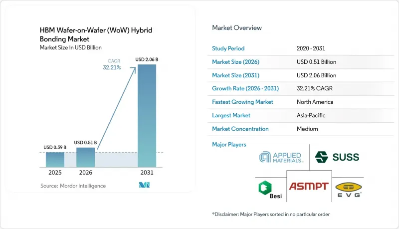
本報告按鍵合架構(例如,晶圓對晶圓)、鍵合類型(例如,銅對銅)、設備類型(例如,晶圓鍵合機)、整合度(例如,2.5D整合)、終端用戶行業(例如,半導體代工廠)、應用領域(例如,存儲器和存儲)以及地區進行細分。市場預測以美元(USD)計價。
全球HBM晶圓級(WoW)混合鍵結市場趨勢及洞察
增加人工智慧加速器中的 HBM 堆疊數量
人工智慧加速器藍圖正推動記憶體堆疊密度的進一步提升,使得垂直互連密度成為HBM晶圓級(WoW)混合鍵結市場的關鍵成長要素。 SK海力士在2026年國際消費電子展(CES 2026)上發表了一款16層HBM4裝置,容量為48GB,頻寬超過2TB/s,目標是在2026年第三季開始量產。三星宣布,透過將1c DRAM製程與混合銅鍵合技術相結合,已將HBM4的運行速度提升至11.7Gb/s,顯著超越了JEDEC 8Gb/s的基準值。發表在《電子學》(Electronics)期刊上的一篇同行評審文章指出,混合鍵合技術可將8層HBM結構的整體堆疊厚度降低15%以上,並透過以直接銅連接取代底部填充物來改善垂直散熱。當層數超過 12 層時,僅靠微凸塊難以控制熱機械應力和封裝高度,這使得 HBM 晶圓疊晶圓 (WoW) 混合鍵合市場與新一代 AI 記憶體程式密切相關。
邏輯和記憶體的共封裝整合
透過將邏輯和記憶體整合到單一鍵合堆疊中,HBM 晶圓疊層 (WoW) 混合鍵合技術在市場上的作用已不再局限於記憶體堆疊。香港科技大學 (HKUST) 的研究表明,採用晶圓疊層 (WoW) 技術的加速器相比 NVIDIA A100基準,推理性能提升高達 7.17 倍;同時,基於晶片組的設計相比單片式方案,迭代工程成本降低了 38.09%。台積電宣布,其 SoIC-X 平台已被 AMD 應用於第二代 3D V-Cache(9µm 間距),頻寬是傳統封裝的 10 倍。應用材料公司表示,其採用 Besi 晶片的 Kinex 平台已在台積電投入量產,用於博通的客製化 AI ASIC,旨在實現下一代系統中 50nm 以上的精度和更高的吞吐量。這些性能和成本優勢相結合意味著,即使純 HBM 的訂單週期出現波動,HBM 晶圓疊晶圓 (WoW) 混合鍵合市場的需求預計仍將保持強勁。
混合鍵結設備的高資本密集度
資本密集度仍是HBM晶圓級(WoW)混合鍵結市場面臨的一大障礙。這是因為僅僅購買一台鍵合機不足以建造一條經過認證的生產線。應用材料公司將混合鍵合定位為涵蓋沉積、化學機械拋光(CMP)和製程控制的製程鏈,這意味著生產線認證需要多個類別的昂貴設備。儘管SUSS MicroTec的XBC300 Gen2平台將晶圓級鍵合、批量晶片到晶圓以及順序晶片到晶圓的功能整合到一個系統中,但其模組化設計仍然使其成為更廣泛的資本投資計劃的一部分,而不是低成本的入門級產品。此外,客戶還需要對鍵合機周圍的清洗、活化、測量和退火過程提供支持,這增加了達到商業級良率所需的最低投資。因此,HBM晶圓級(WoW)混合鍵合市場的應用主要集中在財力雄厚的晶圓代工廠、記憶體製造商和先進封裝公司。
細分市場分析
2025年,晶圓對晶圓鍵結技術在HBM晶圓疊層(WoW)混合鍵結市場中佔68.32%的佔有率。這反映了該技術在成熟半導體應用中強大的生產記錄和高產能。由於該技術可在數秒內完成整個晶圓的鍵合,而單一晶片的放置週期則要長得多,因此它仍然佔據HBM晶圓疊層(WoW)混合鍵合市場的重要佔有率。該技術在3D NAND、CMOS影像感測器和DRAM領域的成功應用,以及其降低尋求可重複製造路線的客戶實施風險的能力,進一步鞏固了其市場地位。 2026年5月,imec和EV Group展示了晶圓對晶圓鍵合技術也可應用於要求更高的邏輯堆疊操作,他們使用GEMINI FB系統在300mm晶圓上實現了200nm間距下低於40nm的銅焊盤套刻精度。
預計到2031年,晶片-晶圓鍵合技術將以32.68%的複合年成長率成長。這是因為在晶片組和HBM設計中,通常需要進行選擇性放置,而非全晶圓配對。當晶圓尺寸有差異、需要處理已驗證功能正常的晶圓,或從良率管理角度來看全晶圓鍵合技術效率低時,此方法特別有效。在2026年歐洲晶片技術大會(ECTC 2026)上,CEA-Leti展示了1µm間距的功能性晶片-晶圓混合鍵合技術,解決了高密度異構AI硬體領域的一個重要技術瓶頸。晶片-晶片鍵合在HBM晶圓-晶圓(WoW)混合鍵合市場中仍然是一個規模較小且更具選擇性的細分市場。這是因為在良率有限的整合案例中,單晶片匹配是合理的,因此晶片-晶片鍵合的經濟效益才能得到最佳體現。
到2025年,銅-銅鍵合將佔據55.06%的市場佔有率,成為HBM晶圓疊層(WoW)混合鍵合市場中用於尖端記憶體和邏輯應用的標準製程。 IEEE對索尼、三星、台積電、SK海力士和東京電子等公司的實施案例研究證實,與基於凸塊的替代方案相比,直接銅-銅鍵合具有更優異的熱性能和電氣性能,同時還能適應小於10µm的間距。這種效能優勢對於HBM和堆疊邏輯至關重要,因為隨著層數的增加,互連密度和熱傳遞的管理難度也越來越大。銅-焊盤和金屬-焊盤鍵合技術仍然是客戶從傳統覆晶過渡到更先進鍵合製程的過渡方案。
預計到2031年,氧化物-氧化物和金屬-氧化物混合鍵結將以32.61%的複合年成長率成長,這反映出人們對光電和感測器整合領域日益成長的興趣,而介電相容性在這些領域至關重要。台積電的SoIC-X採用了具有最佳化SiCN介電層的銅焊盤,imec的200nm間距演示也使用了具有最佳化CMP製程的SiCN。這顯示介電層工程已成為大規模量產級小型化的一部分。因此,鍵合方案的開發更與表面處理、CMP均勻性和套刻控制相關,而非鍵結形成本身。隨著更多異質元件進入HBM晶圓疊層(WoW)混合鍵合市場,簡單的銅介面和完整的材料堆疊之間的差距將繼續縮小。
區域分析
預計到2025年,亞太地區將佔據83.61%的市場佔有率,鞏固其作為HBM晶圓疊層(WoW)混合鍵合市場中心的地位。這一主導地位得益於韓國三星電子和SK海力士、台灣台積電的SOIC平台以及日本作為設備開發和材料供應主要樞紐的地位。這種集中度使得HBM晶圓疊層(WoW)混合鍵合市場與少數已在先進節點規模下運作的記憶體製造商、代工廠和供應商緊密相關。 2025年10月,東京電子宣布投資3.3億美元(以2025年平均外匯計算)在九州興建新的先進封裝設備研發基地。中國也正在開發鍵合相關設備的國產替代方案,反映出出口限制正在重塑供應鏈並刺激本土技術發展。
預計到2031年,北美地區的複合年成長率將達到33.02%,因此,該地區HBM晶圓級(WoW)混合鍵合的市場規模預計將比其他任何地區都更快地成長。主要驅動力是先進封裝和國內半導體製造領域的投資,而這得益於《晶片技術創新法案》(CHIPS Act)的支持。英特爾承諾投入78.6億美元的CHIPS Act津貼,用於支持其在亞利桑那州、新墨西哥州、俄亥俄州和奧勒岡州的工廠。這其中包括與Foveros Direct混合鍵合相關的項目。台積電在亞利桑那州的擴張也凸顯了該地區的重要性,因為人工智慧相關客戶對其國內供應鏈中先進封裝能力的需求日益成長。儘管歐洲的市場佔有率仍然較小,但它仍然透過imec(比利時)、SUSS MicroTec(德國)、Besi(荷蘭)和CEA-Leti(法國)等公司佔據著重要的戰略地位。
由於缺乏支援此類設備的先進半導體製造基礎設施,預計到2025年,南美洲、中東和非洲僅能佔據較小的市場佔有率。它們在HBM晶圓疊層(WoW)混合鍵合市場中的作用可能僅限於提供服務和分銷支持,而非開展大規模的生產或研發活動。因此,預計2026年至2031年間,這些地區不會有顯著的投資需求。
其他好處:
- Excel格式的市場預測(ME)表
- 3個月的分析師支持
目錄
第1章:引言
- 研究假設和市場定義
- 調查範圍
第2章:調查方法
第3章執行摘要
第4章 市場狀況
- 市場概覽
- 市場促進因素
- 增加人工智慧加速器中的 HBM 堆疊數量
- 邏輯和記憶體共封裝
- 過渡到小於10微米的佈線間距
- 前端晶圓級製程控制的實施
- 透過基於晶片的HBM架構中的試點生產線降低風險
- 對光電和感測器協同整合的需求
- 市場限制因素
- 混合黏接模具的高資本密集度
- 對顆粒和表面缺陷的敏感性
- 獲得超精密黏合認證的供應商數量有限。
- 超薄堆疊晶片中熱機械應力的風險
- 產業價值鏈分析
- 監理情勢
- 技術展望
- 波特五力分析
- 宏觀經濟因素對市場的影響
第5章 市場規模與成長預測
- 鍵結架構
- Wafer-to-Wafer
- Die-to-wafer
- Die-to-die
- 按鍵結類型
- 銅 - 銅
- 銅對焊盤和金屬對焊盤
- 氧化物間鍵結和金屬-氧化物雜化鍵結
- 依設備類型
- 晶圓鍵合機
- 表面處理工具
- 檢測和測量工具
- 清洗和CMP設備
- 依整合程度
- 2.5D 整合
- 3D整合
- 晶片整合
- 按最終用戶行業分類
- 半導體晶圓代工廠
- OSAT
- 垂直整合的設備製造商
- 其他終端用戶產業
- 透過使用
- 記憶體和儲存
- 計算與邏輯
- 感測與介面
- 連接與通訊
- 光電和光連接模組
- 按地區
- 北美洲
- 美國
- 加拿大
- 墨西哥
- 歐洲
- 德國
- 英國
- 法國
- 義大利
- 其他歐洲國家
- 亞太地區
- 中國
- 日本
- 韓國
- 台灣
- 印度
- 其他亞太國家
- 南美洲
- 中東和非洲
- 北美洲
第6章 競爭情勢
- 市場集中度
- 策略趨勢
- 市佔率分析
- 公司簡介
- EV Group
- Applied Materials, Inc.
- SUSS MicroTec SE
- BE Semiconductor Industries NV
- ASMPT Limited
- Tokyo Electron Limited
- KLA Corporation
- Onto Innovation Inc.
- Lam Research Corporation
- DISCO Corporation
- SHIBAURA MECHATRONICS CORPORATION
- Hanmi Semiconductor Co., Ltd.
- Toray Engineering Co., Ltd.
- BEIJING U-PRECISION TECH CO., LTD.
- Applied Microengineering Ltd.
- SET Corporation SA
- Piotech, Inc.
- NAURA Technology Group Co., Ltd.
- Nidec Machine Tool Corporation
第7章 市場機會與未來展望
According to Mordor Intelligence, the HBM wafer-on-Wafer (wow) hybrid bonding market size stood at USD 0.39 billion in 2025 and is forecast to reach USD 2.06 billion by 2031, growing at a CAGR of 32.21% over 2026-2031.
This report is Segmented by Bonding Architecture (Wafer-To-Wafer, and More), Bonding Type (Copper-To-Copper, and More), Equipment Type (Wafer Bonders, and More), Integration Level (2. 5D Integration, and More), End-User Industry (Semiconductor Foundries, and More), Application (Memory and Storage, and More), and Geography. The Market Forecasts are Provided in Terms of Value (USD).
Global HBM Wafer-on-Wafer (WoW) Hybrid Bonding Market Trends and Insights
Rising HBM Stack Counts in AI Accelerators
AI accelerator roadmaps are pushing memory stack counts higher, making vertical interconnect density a central growth driver for the HBM Wafer-on-Wafer (WoW) hybrid bonding market. SK hynix unveiled a 16-layer HBM4 device with 48GB capacity and bandwidth above 2TB per second at CES 2026, and the company targeted mass production in the third quarter of 2026. Samsung disclosed HBM4 operating speeds of 11.7Gb/s by combining its 1c DRAM process with hybrid copper bonding, which placed it well above the JEDEC baseline of 8Gb/s. A peer-reviewed review in Electronics found that hybrid bonding reduced total stack height by more than 15% in an 8-layer HBM structure and improved vertical heat transfer by replacing underfill with direct copper connections. As stack counts exceed 12 layers, thermomechanical stress and package height become harder to manage with microbumps alone, so the HBM Wafer-on-Wafer (WoW) hybrid bonding market remains closely linked to next-generation AI memory programs.
Co-Packaged Logic and Memory Integration
Co-integrating logic and memory in a single bonded stack is expanding the role of the HBM Wafer-on-Wafer (WoW) hybrid bonding market beyond pure memory stacking. HKUST research showed that wafer-on-wafer stacked accelerators delivered inference up to 7.17 times faster than an NVIDIA A100 baseline, while chiplet-based designs reduced recurring engineering costs by 38.09% compared with monolithic alternatives. TSMC stated that its SoIC-X platform was used in AMD's second-generation 3D V-Cache at 9µm pitch and delivered 10 times the bandwidth of conventional packaging. Applied Materials said its Kinex platform with Besi is already in mass production at TSMC for Broadcom custom AI ASICs, and the next-generation system targets 50nm accuracy or better with higher throughput. This combination of performance and cost benefits means the HBM Wafer-on-Wafer (WoW) hybrid bonding market can sustain demand even when pure HBM order cycles fluctuate.
High Capital Intensity of Hybrid Bonding Tooling
Capital intensity remains a real brake on the HBM Wafer-on-Wafer (WoW) hybrid bonding market because qualified production lines require more than a single bonder purchase. Applied Materials positioned hybrid bonding as a process chain spanning deposition, CMP, and process control, indicating that line qualification requires multiple categories of high-value equipment. SUSS MicroTec's XBC300 Gen2 platform combines wafer-to-wafer, collective die-to-wafer, and sequential die-to-wafer capability in one system, but that modularity still sits within a broader capital program rather than a low-cost entry point. Customers also need cleaning, activation, metrology, and annealing support around the bonder, which increases the minimum spend required before commercial yields can be achieved. This keeps adoption concentrated among the most capitalized foundries, memory makers, and advanced packaging operators in the HBM Wafer-on-Wafer (WoW) hybrid bonding market.
Other drivers and restraints analyzed in the detailed report include:
- Sub-10 Micron Interconnect Pitch Migration
- Front-End Wafer-Level Process Control Adoption
- Yield Sensitivity to Particle and Surface Defects
For complete list of drivers and restraints, kindly check the Table Of Contents.
Segment Analysis
Wafer-to-wafer held 68.32% of the HBM Wafer-on-Wafer (WoW) hybrid bonding market share in 2025, reflecting its strong production record and higher throughput in established semiconductor applications. The architecture remained the larger part of the HBM Wafer-on-Wafer (WoW) hybrid bonding market because it can bond an entire wafer in seconds rather than placing individual dies over much longer cycle times. Its position was also supported by proven use in 3D NAND, CMOS image sensors, and DRAM, thereby reducing adoption risk for customers seeking a repeatable manufacturing route. In May 2026, imec and EV Group demonstrated less than 40nm Cu pad overlay accuracy across a full 300mm wafer at a 200nm pitch on the GEMINI FB system, demonstrating that wafer-to-wafer bonding can move into much more demanding logic stacking work.
Die-to-wafer is projected to grow at a 32.68% CAGR through 2031 because chiplet and HBM designs often need selective placement rather than full-wafer pairing. The approach is especially relevant when die sizes differ, when handling known-good dies matters, or when yield management makes full-wafer bonding inefficient. CEA-Leti demonstrated functional die-to-wafer hybrid bonding at a 1µm pitch at ECTC 2026, removing a key technical bottleneck for high-density heterogeneous AI hardware. Die-to-die bonding remained a smaller and more selective part of the HBM Wafer-on-Wafer (WoW) hybrid bonding market because its economics work best in limited-yield integration cases where single-die matching is justified.
Copper-to-Copper bonding captured 55.06% of the market share in 2025, making it the reference process in the HBM Wafer-on-Wafer (WoW) hybrid bonding market for leading-edge memory and logic applications. An IEEE research review of implementations across Sony, Samsung, TSMC, SK hynix, and Tokyo Electron confirmed that direct Cu-Cu bonding supports pitches below 10µm while offering stronger thermal and electrical performance than bump-based alternatives. That performance advantage matters in HBM and stacked logic because both interconnect density and heat transfer become harder to manage as layer counts increase. Copper-to-pad and metal-to-pad routes continue to serve as transitional options for customers moving from conventional flip-chip to more advanced bonding flows.
Oxide-to-Oxide and Metal-Oxide Hybrid Bonding is projected to grow at a 32.61% CAGR through 2031, reflecting rising interest in photonics and sensor integration, where dielectric compatibility is essential. TSMC's SoIC-X uses an optimized SiCN dielectric with Cu pads, and imec's 200nm pitch demonstration also used SiCN with an optimized CMP flow, demonstrating that dielectric engineering is already part of production-grade scaling. This keeps bonding type development tightly linked to surface preparation, CMP uniformity, and overlay control rather than to bond formation alone. As more heterogeneous devices move into the HBM Wafer-on-Wafer (WoW) hybrid bonding market, the gap between a simple copper interface and a full materials stack will keep narrowing.
Complete Report Scope:
- By Bonding Architecture
- Wafer-to-Wafer
- Die-to-Wafer
- Die-to-Die
- By Bonding Type
- Copper-to-Copper
- Copper-to-Pad and Metal-to-Pad
- Oxide-to-Oxide and Metal-Oxide Hybrid Bonding
- By Equipment Type
- Wafer Bonders
- Surface Preparation Tools
- Inspection and Metrology Tools
- Cleaning and CMP Systems
- By Integration Level
- 2.5D Integration
- 3D Integration
- Chiplet Integration
- By End User Industry
- Semiconductor Foundries
- OSATs
- Integrated Device Manufacturers
- Other End-user Industries
- By Application
- Memory and Storage
- Computing and Logic
- Sensing and Interface
- Connectivity and Communications
- Photonics and Optical Interconnects
- By Geography
- North America
- United States
- Canada
- Mexico
- Europe
- Germany
- United Kingdom
- France
- Italy
- Rest of Europe
- Asia-Pacific
- China
- Japan
- South Korea
- Taiwan
- India
- Rest of Asia-Pacific
- South America
- Middle East and Africa
- North America
Geography Analysis
Asia-Pacific held an 83.61% share in 2025, making it the clear center of the HBM Wafer-on-Wafer (WoW) hybrid bonding market. The region leads because South Korea houses Samsung Electronics and SK hynix, Taiwan hosts TSMC's SoIC platform, and Japan remains a major base for equipment development and materials supply. This concentration keeps the HBM Wafer-on-Wafer (WoW) hybrid bonding market closely tied to a compact group of memory manufacturers, foundries, and equipment vendors that already operate at advanced-node scale. Tokyo Electron announced a USD 330 million investment in October 2025 to build a new advanced packaging equipment development hub in Kyushu, at the 2025 average exchange rate used as input. China is also building domestic alternatives in bonding-related equipment, which reflects how export controls are reshaping the supply chain and encouraging local capability development.
North America is projected to post a 33.02% CAGR through 2031, and its HBM Wafer-on-Wafer (WoW) hybrid bonding market size is therefore set to expand faster than any other region. The main driver is the CHIPS Act-backed investment in advanced packaging and domestic semiconductor manufacturing. Intel finalized a USD 7.86 billion CHIPS Act funding award to support sites in Arizona, New Mexico, Ohio, and Oregon, including programs tied to Foveros Direct hybrid bonding. TSMC's Arizona expansion also supports the regional case because AI customers increasingly want advanced packaging capacity inside a domestic supply chain. Europe remains smaller in share, but it stays strategically relevant through imec in Belgium, SUSS MicroTec in Germany, Besi in the Netherlands, and CEA-Leti in France.
South America and the Middle East and Africa held only a negligible position in 2025 because they lack leading-edge semiconductor manufacturing infrastructure for this equipment class. Their role in the HBM Wafer-on-Wafer (WoW) hybrid bonding market is more likely to stay limited to service coverage and distribution support than to primary production or research activity. This means meaningful investment demand from these regions is not expected to emerge within the 2026-2031 period.
- EV Group
- Applied Materials, Inc.
- SUSS MicroTec SE
- BE Semiconductor Industries N.V.
- ASMPT Limited
- Tokyo Electron Limited
- KLA Corporation
- Onto Innovation Inc.
- Lam Research Corporation
- DISCO Corporation
- SHIBAURA MECHATRONICS CORPORATION
- Hanmi Semiconductor Co., Ltd.
- Toray Engineering Co., Ltd.
- BEIJING U-PRECISION TECH CO., LTD.
- Applied Microengineering Ltd.
- SET Corporation SA
- Piotech, Inc.
- NAURA Technology Group Co., Ltd.
- Nidec Machine Tool Corporation
Additional Benefits:
- The market estimate (ME) sheet in Excel format
- 3 months of analyst support
TABLE OF CONTENTS
1 INTRODUCTION
- 1.1 Study Assumptions and Market Definition
- 1.2 Scope of the Study
2 RESEARCH METHODOLOGY
3 EXECUTIVE SUMMARY
4 MARKET LANDSCAPE
- 4.1 Market Overview
- 4.2 Market Drivers
- 4.2.1 Rising HBM Stack Counts in AI Accelerators
- 4.2.2 Co-Packaged Logic and Memory Integration
- 4.2.3 Sub-10 Micron Interconnect Pitch Migration
- 4.2.4 Front-End Wafer-Level Process Control Adoption
- 4.2.5 Pilot-Line De-Risking for Chiplet-Based HBM Architectures
- 4.2.6 Photonics and Sensor Co-Integration Demand
- 4.3 Market Restraints
- 4.3.1 High Capital Intensity of Hybrid Bonding Tooling
- 4.3.2 Yield Sensitivity to Particle and Surface Defects
- 4.3.3 Limited Qualified Supplier Base for Ultra-Precision Bonding
- 4.3.4 Thermo-Mechanical Stress Risks in Ultra-Thin Stacked Dies
- 4.4 Industry Value Chain Analysis
- 4.5 Regulatory Landscape
- 4.6 Technological Outlook
- 4.7 Porter's Five Forces Analysis
- 4.7.1 Bargaining Power of Suppliers
- 4.7.2 Bargaining Power of Buyers
- 4.7.3 Threat of New Entrants
- 4.7.4 Threat of Substitutes
- 4.7.5 Intensity of Competitive Rivalry
- 4.8 Impact of Macroeconomic Factors on the Market
5 MARKET SIZE AND GROWTH FORECASTS (VALUE)
- 5.1 By Bonding Architecture
- 5.1.1 Wafer-to-Wafer
- 5.1.2 Die-to-Wafer
- 5.1.3 Die-to-Die
- 5.2 By Bonding Type
- 5.2.1 Copper-to-Copper
- 5.2.2 Copper-to-Pad and Metal-to-Pad
- 5.2.3 Oxide-to-Oxide and Metal-Oxide Hybrid Bonding
- 5.3 By Equipment Type
- 5.3.1 Wafer Bonders
- 5.3.2 Surface Preparation Tools
- 5.3.3 Inspection and Metrology Tools
- 5.3.4 Cleaning and CMP Systems
- 5.4 By Integration Level
- 5.4.1 2.5D Integration
- 5.4.2 3D Integration
- 5.4.3 Chiplet Integration
- 5.5 By End User Industry
- 5.5.1 Semiconductor Foundries
- 5.5.2 OSATs
- 5.5.3 Integrated Device Manufacturers
- 5.5.4 Other End-user Industries
- 5.6 By Application
- 5.6.1 Memory and Storage
- 5.6.2 Computing and Logic
- 5.6.3 Sensing and Interface
- 5.6.4 Connectivity and Communications
- 5.6.5 Photonics and Optical Interconnects
- 5.7 By Geography
- 5.7.1 North America
- 5.7.1.1 United States
- 5.7.1.2 Canada
- 5.7.1.3 Mexico
- 5.7.2 Europe
- 5.7.2.1 Germany
- 5.7.2.2 United Kingdom
- 5.7.2.3 France
- 5.7.2.4 Italy
- 5.7.2.5 Rest of Europe
- 5.7.3 Asia-Pacific
- 5.7.3.1 China
- 5.7.3.2 Japan
- 5.7.3.3 South Korea
- 5.7.3.4 Taiwan
- 5.7.3.5 India
- 5.7.3.6 Rest of Asia-Pacific
- 5.7.4 South America
- 5.7.5 Middle East and Africa
- 5.7.1 North America
6 COMPETITIVE LANDSCAPE
- 6.1 Market Concentration
- 6.2 Strategic Moves
- 6.3 Market Share Analysis
- 6.4 Company Profiles (includes Global Level Overview, Market Level Overview, Core Segments, Financials as available, Strategic Information, Market Rank/Share, Products and Services, Recent Developments)
- 6.4.1 EV Group
- 6.4.2 Applied Materials, Inc.
- 6.4.3 SUSS MicroTec SE
- 6.4.4 BE Semiconductor Industries N.V.
- 6.4.5 ASMPT Limited
- 6.4.6 Tokyo Electron Limited
- 6.4.7 KLA Corporation
- 6.4.8 Onto Innovation Inc.
- 6.4.9 Lam Research Corporation
- 6.4.10 DISCO Corporation
- 6.4.11 SHIBAURA MECHATRONICS CORPORATION
- 6.4.12 Hanmi Semiconductor Co., Ltd.
- 6.4.13 Toray Engineering Co., Ltd.
- 6.4.14 BEIJING U-PRECISION TECH CO., LTD.
- 6.4.15 Applied Microengineering Ltd.
- 6.4.16 SET Corporation SA
- 6.4.17 Piotech, Inc.
- 6.4.18 NAURA Technology Group Co., Ltd.
- 6.4.19 Nidec Machine Tool Corporation
7 MARKET OPPORTUNITIES AND FUTURE OUTLOOK
- 7.1 White-Space and Unmet-Need Assessment

 半導體鍵結市場:依類型、技術、應用、最終用戶、國家及地區分類-產業分析、市場規模、市場佔有率及2026年至2033年預測
 半導體鍵合設備:市場佔有率分析、產業趨勢與統計、成長預測(2026-2031)
 半導體鍵結市場-2026-2032年全球市場預測
 半導體鍵結設備市場商機、成長要素、產業趨勢分析及2026-2035年預測。半導體鍵結:市場佔有率分析、產業趨勢與統計、成長預測(2026-2031)
 半導體晶圓鍵合技術市場分析及預測至 2035 年:按類型、產品類型、技術、應用、材料類型、製程、最終用戶、設備和解決方案分類。半導體鍵結市場分析及預測(至2035年):類型、產品、技術、應用、材料類型、裝置、製程、最終用戶、設備、解決方案
 半導體鍵結市場規模、佔有率、成長及全球產業分析:依類型、應用和地區劃分的洞察與預測(2026-2034年)
 半導體鍵結市場-全球產業規模、佔有率、趨勢、機會與預測:按類型、製程類型、鍵結技術、應用、地區和競爭格局分類,2021-2031年
 半導體鍵合市場,按鍵合技術、鍵結材料、最終用戶和地區分類