

 |
市場調查報告書
商品編碼
2062073
半導體鍵結:市場佔有率分析、產業趨勢與統計、成長預測(2026-2031)Semiconductor Bonding - Market Share Analysis, Industry Trends & Statistics, Growth Forecasts (2026 - 2031) |
||||||
※ 本網頁內容可能與最新版本有所差異。詳細情況請與我們聯繫。
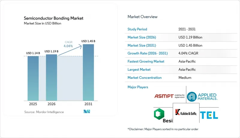
根據 Mordor Intelligence 預測,半導體鍵結市場規模將從 2025 年的 11.4 億美元成長到 2026 年的 11.9 億美元,到 2031 年將達到 14.5 億美元,2026 年至 2031 年的複合年成長率為 4.04%。
本報告按設備類型(晶片鍵合機、晶圓鍵合機等)、互連等級(晶片間互連等)、應用領域(MEMS和感測器等)、終端用戶產業(家用電子電器、汽車及出行等)以及地區(亞太地區、北美、歐洲、南美、中東和非洲)進行細分。市場預測以美元計價。
全球半導體鍵結市場趨勢及洞察
對先進封裝和小型化的需求日益成長
異構晶片組使代工廠能夠以小於 10微米的間距堆疊邏輯、記憶體和類比晶片,從而消除微凸塊並將寄生電容降低 80%。 UCIe 3.0 提供 64 GT/s 的連結,為 AI 加速器提供每平方毫米高達 4 TB/s 的頻寬。 Intel Foveros Direct 的互連密度是覆晶構裝的 15 倍,並支援資料中心模組 300 W 的熱設計功耗 (TDE)。玻璃基板正進入原型製作階段,其翹曲度僅為有機材料的十分之一,面板級成本降低了 30%。因此,半導體鍵合市場對整合等離子體活化、對準和熱壓縮叢集的混合鍵合機的訂單創下歷史新高。
家用電子電器和汽車產業的擴張
晶圓級晶片封裝技術使CMOS(互補型金屬氧化物半導體)影像感測器的高度降低了40%,從而實現了更薄的智慧型手機和多相機汽車。預計到2029年,汽車CIS(影像資訊系統)的出貨量將達到12億台,銷售額將達到84億美元。碳化矽(SiC)牽引逆變器需要能夠承受200 度C高溫的晶片貼裝技術,這使得燒結銀在新電動車平台的應用率超過了50%。銅線目前已佔汽車鍵合的38%,隨著AEC-Q006製程的成熟,預計到2027年這一比例將超過45%。隨著高功率模組和光學模組被納入先進封裝流程,這些趨勢正在擴大市場。
高資本投資及營運成本
混合鍵合設備的單價在500萬至800萬美元之間,整條生產線的成本超過3000萬美元,這給OSAT(半導體組裝外包商)平均10%的利潤率帶來了壓力。由於設計規則會持續演變以滿足客戶的認證要求,初始運轉率仍維持在50%左右,投資回收期長達三年以上。美國和歐洲的人事費用比亞洲高出40%至50%,而CMP(化學機械拋光)耗材的成本為每片晶圓15至20美元,是覆晶底部填充材料成本的三倍,這進一步增加了營運成本。這些因素限制了半導體鍵結市場短期內的擴張。
細分市場分析
預計到2025年,晶片鍵合設備將佔銷售額的36.77%,因為高精度共晶和環氧樹脂鍵合仍然是功率和射頻元件的核心。覆晶鍵合機可處理40至150微米的間距,產能超過每小時5000片;而引線鍵合機則在對成本敏感的組裝應用中佔據主導地位。晶圓鍵合機支援MEMS和3D NAND技術,與晶片級封裝相比,可節省30-40%的成本,從而支撐傳統裝置的半導體鍵合市場規模。
預計到2031年,混合鍵合機將以4.27%的最高複合年成長率成長,因為它們是實現HBM4、晶片組和共封裝光學元件10µm以下間距的必要設備。 EV集團的GEMINI平台可施加350 kN的力進行無助焊劑鍵合,而Applied-Besi Kinex叢集可將週期時間縮短40%。台積電的CoWoS量產涉及約250台設備,價值約15億美元,顯示市場擁有強大的投資意願。即使晶片貼裝線的運轉率很高,市場仍在將支出重新分配到混合叢集設備上。
UCIe 標準將頻寬提升至 4 TB/s mm²,使 AI 加速器能夠將邏輯晶片和 HBM4 晶片組合在一起,從而使晶片間鍵合技術在 2025 年佔據 53.91% 的市場佔有率。英特爾的 EMIB 技術無需使用完整的中介層即可連接間距為 55µm 的晶片,而 Amkor 目前在亞利桑那州和韓國提供 EMIB 技術。這種拓撲結構構成了 2026-2029 年藍圖的基礎,並確保了半導體鍵合市場的最大佔有率。
隨著3D NAND快閃記憶體層數突破400層,並向1000層堆疊結構邁進,晶圓間混合鍵結技術預計在預測期(2026-2031年)內將以4.52%的複合年成長率成長。三星、長江儲存和鎧俠等公司均在晶圓級將CMOS邏輯晶片鍵合到記憶體下方,將良率提高25%。晶片間晶圓鍵合技術支援CIS和射頻元件,將功能正常的晶片安裝到被動晶圓上。這些整合流程正在拓展半導體鍵結市場在記憶體、邏輯晶片和感測器節點上的覆蓋範圍。
區域分析
預計到2025年,亞太地區將佔全球銷售額的41.53%,並將在2031年之前以4.91%的複合年成長率成長,增速位居各地區之首。台積電計畫在2026年將其CoWoS晶圓產能從每月1.2萬片提升至每月5萬片,並已開始建造其位於嘉義的AI加速器工廠。韓國正投資2,300億美元用於三星電子位於龍仁的工廠和SK海力士位於P&T7的工廠,目標是到2028年將國內HBM產能提高三倍。中國的232層NAND快閃記憶體「XTacking」技術正在規避出口限制,而日本則向東京電子的研發部門投資93億美元(1.5兆日圓)。區域供應集中化透過整合熟練勞動力、供應商和補貼,正在重振半導體鍵合市場。
北美已從《晶片技術創新法案》(CHIPS Act)中獲得364億美元的津貼,其中安姆科(Amcor)位於亞利桑那州的工廠和SK海力士位於印第安納州的HBM生產線構成了其先進封裝能力的核心。英特爾將EMIB封裝外包給安姆科,而美光(Micron)已投資18億美元用於PSMC的P5晶圓廠,以擴大DRAM產能。墨西哥正利用其人事費用比美國低60%的優勢,吸引企業將引線焊線業務近岸外包,將其運往德克薩斯州晶圓廠的物流時間縮短了40%。這項政策著重於封裝而非光刻,為北美市場的強勁成長奠定了基礎。
歐洲透過IPCEI-ME計畫獲得了430億歐元(486.2億美元)的資金,其中25億歐元(28.3億美元)分配給了NanoIC混合鍵結套件。台積電正在德勒斯登投資100億歐元(113.1億美元)建造其300毫米晶圓廠,該晶圓廠計劃於2027年運作;英特爾則計劃於2029年在其馬格德堡工廠開始初步生產。儘管授權流程比亞洲市場落後18至24個月,但資金流入正在擴大當地的鍵結需求。南美洲仍專注於傳統技術,而中東的專案仍處於探索階段。綜上所述,這些因素表明,儘管半導體鍵結市場仍集中在亞洲,但其地緣政治格局正趨於多元化。
其他好處:
- Excel格式的市場預測(ME)表
- 3個月的分析師支持
目錄
第1章:引言
- 研究假設和市場定義
- 調查範圍
第2章:調查方法
第3章執行摘要
第4章 市場狀況
- 市場概覽
- 市場促進因素
- 對先進封裝和小型化的需求日益成長
- 家用電器和汽車產業的擴張
- 3D整合技術與MEMS裝置的廣泛應用
- 面向邊緣運算的AI主導異質整合
- 政府對半導體補貼的競爭正在重塑區域債券發行能力。
- 市場限制因素
- 高資本投資及營運成本
- 高階節點的製程複雜性
- 用於混合鍵結的超平晶圓供不應求
- 價值鏈分析
- 波特五力模型
第5章 市場規模與成長預測
- 依設備類型
- 晶片鍵合裝置
- 晶圓鍵合設備
- 覆晶鍵合裝置
- 引線鍵合裝置
- 混合鍵結系統
- 互連等級
- 晶片黏接
- 晶片到晶圓的鍵合
- 晶圓鍵合
- 透過使用
- 射頻設備
- 微機電系統和感測器
- CMOS影像感測器
- LED
- 3D NAND
- 產業最終用途
- 家用電子產品
- 汽車與出行
- 工業自動化
- 醫療保健和生命科學
- 電訊和資料通訊
- 航太/國防
- 其他終端用戶產業(能源及其他)
- 按地區
- 亞太地區
- 中國
- 日本
- 印度
- 韓國
- 台灣
- 其他亞太國家
- 北美洲
- 美國
- 加拿大
- 墨西哥
- 南美洲
- 巴西
- 阿根廷
- 其他南美國家
- 歐洲
- 德國
- 英國
- 法國
- 義大利
- 俄羅斯
- 其他歐洲國家
- 中東和非洲
- 沙烏地阿拉伯
- 南非
- 中東和非洲
- 亞太地區
第6章 競爭情勢
- 市場集中度
- 策略趨勢
- 市佔率和排名分析
- 公司簡介
- ADVANTEST CORPORATION
- Amkor Technology
- Applied Materials, Inc.
- ASMPT
- Besi
- EV Group(EVG)
- HANMI INCHEON
- Hesse GmbH
- Kulicke and Soffa Industries, Inc
- Mycronic
- Nitto Denko Corporation
- Nordson Corporation
- Onto Innovation
- Palomar Technologies
- SHINKO ELECTRIC INDUSTRIES
- SUSS MicroTec SE
- Tokyo Electron Limited
- TORAY ENGINEERING Co., Ltd.
- TPT Wire Bonder GmbH & Co KG
- Yamaha Robotics
第7章 市場機會與未來展望
According to Mordor Intelligence, the semiconductor bonding market size is expected to grow from USD 1.14 billion in 2025 to USD 1.19 billion in 2026 and is forecast to reach USD 1.45 billion by 2031 at 4.04% CAGR over 2026-2031.
This report is Segmented by Equipment Type (Die Bonder, Wafer Bonder, and More), Interconnect Level (Die-To-Die, and More), Application (MEMS and Sensors, and More), End-Use Industry (Consumer Electronics, Automotive and Mobility, and More), and Geography (Asia-Pacific, North America, Europe, South America, and Middle East and Africa). The Market Forecasts are Provided in Terms of Value (USD).
Global Semiconductor Bonding Market Trends and Insights
Growing Demand for Advanced Packaging and Miniaturization
Heterogeneous chiplets allow foundries to stack logic, memory, and analog dies at sub-10 micrometer pitches, removing micro-bumps and lowering parasitic capacitance by 80%. UCIe 3.0 enables 64 GT/s links, giving AI accelerators up to 4 TB/s bandwidth per square millimeter. Intel Foveros Direct reaches 15 times the interconnect density of flip-chip packaging, supporting 300 W thermal-design envelopes for datacenter tiles. Glass substrates enter pilot production with 10-times lower warpage than organic materials and cut panel-level cost by 30%. As a result, the semiconductor bonding market attracts record orders for hybrid bonders that integrate plasma activation, alignment, and thermocompression in one tool cluster.
Expansion of Consumer Electronics and Automotive Sectors
Wafer-level chip-scale packaging shrinks CMOS (Complementary Metal-Oxide-Semiconductor) image-sensor height by 40%, enabling thinner phones and multi-camera vehicles. Automotive CIS shipments are projected to hit 1.2 billion units by 2029, equivalent to USD 8.4 billion in revenue. Silicon carbide traction inverters need die-attach that survives 200°C, pushing adoption of sintered silver past 50% share in new EV platforms. Copper wire already represents 38% of automotive bonds and will pass 45% by 2027 as AEC-Q006 processes mature. These trends expand the market by drawing high-power and optical modules into advanced-packaging flows.
High Capital Investment and Operational Costs
Hybrid-bonding tools cost USD 5-8 million each, and a full line tops USD 30 million, straining OSAT (Outsourced Semiconductor Assembly and Test) margins that average 10%. Early utilization stays near 50% because design rules evolve alongside customer qualifications, stretching payback beyond three years. Labor in the United States and Europe is 40-50% pricier than in Asia, and CMP consumables run USD 15-20 per wafer, triple flip-chip underfill expense, pressuring opex. These factors temper near-term expansion of the semiconductor bonding market.
Other drivers and restraints analyzed in the detailed report include:
- Rising Adoption of 3D Integration and MEMS Devices
- AI-Driven Heterogeneous Integration for Edge Computing
- Process Complexity at Advanced Nodes
For complete list of drivers and restraints, kindly check the Table Of Contents.
Segment Analysis
Die Bonder Equipment retained 36.77% of 2025 revenue as high-precision eutectic and epoxy attach remain core for power and RF components. Flip-chip bonders address 40-150 µm pitches at volumes over 5,000 units per hour, while wire bonders dominate cost-sensitive assemblies. Wafer bonders enable MEMS and 3D NAND with 30-40% cost savings over die-level capping, anchoring the semiconductor bonding market size for legacy devices.
Hybrid bonders will post the quickest 4.27% CAGR through 2031 because HBM4, chiplets, and co-packaged optics require less than 10 µm pitches. EV Group's GEMINI platform applies 350 kN forces for flux-free bonding, and the Applied-Besi Kinex cluster cuts cycle time by 40%. TSMC's CoWoS ramp consumed about 250 tools valued at nearly USD 1.5 billion, confirming capital appetite. The market reallocates spend toward hybrid cluster tools even while die-attach lines run at high utilization.
Die-to-die bonding controlled 53.91% of 2025 revenue because UCIe standards lift bandwidth to 4 TB/s mm2, letting AI accelerators pair logic with HBM4 tiles. Intel EMIB connects dies at 55 µm pitch without full interposers, and Amkor now offers EMIB in Arizona and Korea. This topology anchors 2026-2029 roadmaps and secures the largest semiconductor bonding market share.
Wafer-to-wafer hybrid bonding is projcted to grow at 4.52% CAGR during the forecast period (2026-2031) as 3D NAND sails past 400 layers and targets 1,000-layer stacks. Samsung, YMTC, and Kioxia all bond CMOS logic under memory at the wafer level, improving yield by 25%. Die-to-wafer bonding supports CIS and RF devices where known-good dies mount onto passive wafers. These combined flows reinforce the semiconductor bonding market breadth across memory, logic, and sensor nodes.
Geography Analysis
Asia-Pacific generated 41.53% of 2025 revenue and is forecast to grow 4.91% CAGR through 2031, the highest regional pace. TSMC raised CoWoS capacity from 12,000 to 50,000 wafers per month by 2026 and broke ground on a Chiayi fab aimed at AI accelerators. South Korea's USD 230 billion plan funds Samsung Yongin and SK Hynix P&T7, tripling domestic HBM output by 2028. China's XTacking 232-layer NAND avoids restricted tools, while Japan funnels JPY 1.5 trillion (USD 9.3 billion) into Tokyo Electron research and development. Regional supply concentration feeds the semiconductor bonding market by pooling skilled labor, suppliers, and subsidies.
North America benefits from USD 36.4 billion CHIPS Act grants, with Amkor's Arizona plant and SK Hynix's Indiana HBM line anchoring advanced-packaging capacity. Intel outsources EMIB packaging to Amkor, and Micron paid USD 1.8 billion for PSMC's P5 fab to expand DRAM volume. Mexico draws nearshoring wire-bonding jobs at 60% lower labor cost, trimming logistics times to Texas fabs by 40%. The policy focuses on packaging, versus lithography, and positions the market for resilient North American growth.
Europe secured EUR 43 billion (USD 48.62 billion) under IPCEI-ME, with EUR 2.5 billion (USD 2.83 billion) for NanoIC hybrid-bonding kits. TSMC commits EUR 10 billion (USD 11.31 billion) for a 300 mm fab in Dresden, starting 2027, and Intel's Magdeburg site targets initial output by 2029. Although timelines extend 18-24 months longer than in Asia due to permitting, the capital inflow enlarges local bonding demand. South America remains legacy-focused, and Middle East projects are exploratory. Net impact keeps the semiconductor bonding market concentrated in Asia yet diversifies geopolitical footprints.
- ADVANTEST CORPORATION
- Amkor Technology
- Applied Materials, Inc.
- ASMPT
- Besi
- EV Group (EVG)
- HANMI INCHEON
- Hesse GmbH
- Kulicke and Soffa Industries, Inc
- Mycronic
- Nitto Denko Corporation
- Nordson Corporation
- Onto Innovation
- Palomar Technologies
- SHINKO ELECTRIC INDUSTRIES
- SUSS MicroTec SE
- Tokyo Electron Limited
- TORAY ENGINEERING Co., Ltd.
- TPT Wire Bonder GmbH & Co KG
- Yamaha Robotics
Additional Benefits:
- The market estimate (ME) sheet in Excel format
- 3 months of analyst support
TABLE OF CONTENTS
1 Introduction
- 1.1 Study Assumptions and Market Definition
- 1.2 Scope of the Study
2 Research Methodology
3 Executive Summary
4 Market Landscape
- 4.1 Market Overview
- 4.2 Market Drivers
- 4.2.1 Growing demand for advanced packaging and miniaturization
- 4.2.2 Expansion of consumer electronics and automotive sectors
- 4.2.3 Rising adoption of 3D integration and MEMS devices
- 4.2.4 AI-driven heterogeneous integration for edge computing
- 4.2.5 Government semiconductor subsidy races reshaping regional bonding capacity
- 4.3 Market Restraints
- 4.3.1 High capital investment and operational costs
- 4.3.2 Process complexity at advanced nodes
- 4.3.3 Limited availability of ultra-flat wafers for hybrid bonding
- 4.4 Value Chain Analysis
- 4.5 Porter's Five Forces
- 4.5.1 Threat of New Entrants
- 4.5.2 Bargaining Power of Buyers
- 4.5.3 Bargaining Power of Suppliers
- 4.5.4 Threat of Substitutes
- 4.5.5 Competitive Rivalry
5 Market Size and Growth Forecasts (Value)
- 5.1 By Equipment Type
- 5.1.1 Die Bonder Equipment
- 5.1.2 Wafer Bonder Equipment
- 5.1.3 Flip-Chip Bonder Equipment
- 5.1.4 Wire Bonder Equipment
- 5.1.5 Hybrid Bonder Equipment
- 5.2 By Interconnect Level
- 5.2.1 Die-to-Die Bonding
- 5.2.2 Die-to-Wafer Bonding
- 5.2.3 Wafer-to-Wafer Bonding
- 5.3 By Application
- 5.3.1 RF Devices
- 5.3.2 MEMS and Sensors
- 5.3.3 CMOS Image Sensors
- 5.3.4 LED
- 5.3.5 3D NAND
- 5.4 By End-use Industry
- 5.4.1 Consumer Electronics
- 5.4.2 Automotive and Mobility
- 5.4.3 Industrial and Automation
- 5.4.4 Healthcare and Life-Sciences
- 5.4.5 Telecommunications and Datacom
- 5.4.6 Aerospace and Defense
- 5.4.7 Other End-user Industries (Energy and More)
- 5.5 By Geography
- 5.5.1 Asia-Pacific
- 5.5.1.1 China
- 5.5.1.2 Japan
- 5.5.1.3 India
- 5.5.1.4 South Korea
- 5.5.1.5 Taiwan
- 5.5.1.6 Rest of APAC
- 5.5.2 North America
- 5.5.2.1 United States
- 5.5.2.2 Canada
- 5.5.2.3 Mexico
- 5.5.3 South America
- 5.5.3.1 Brazil
- 5.5.3.2 Argentina
- 5.5.3.3 Rest of South America
- 5.5.4 Europe
- 5.5.4.1 Germany
- 5.5.4.2 United Kingdom
- 5.5.4.3 France
- 5.5.4.4 Italy
- 5.5.4.5 Russia
- 5.5.4.6 Rest of Europe
- 5.5.5 Middle-East and Africa
- 5.5.5.1 Saudi Arabia
- 5.5.5.2 South Africa
- 5.5.5.3 Middle-East and Africa
- 5.5.1 Asia-Pacific
6 Competitive Landscape
- 6.1 Market Concentration
- 6.2 Strategic Moves
- 6.3 Market Share(%)/Ranking Analysis
- 6.4 Company Profiles (includes Global-level Overview, Market-level Overview, Core Segments, Financials as available, Strategic Information, Products and Services, Recent Developments)
- 6.4.1 ADVANTEST CORPORATION
- 6.4.2 Amkor Technology
- 6.4.3 Applied Materials, Inc.
- 6.4.4 ASMPT
- 6.4.5 Besi
- 6.4.6 EV Group (EVG)
- 6.4.7 HANMI INCHEON
- 6.4.8 Hesse GmbH
- 6.4.9 Kulicke and Soffa Industries, Inc
- 6.4.10 Mycronic
- 6.4.11 Nitto Denko Corporation
- 6.4.12 Nordson Corporation
- 6.4.13 Onto Innovation
- 6.4.14 Palomar Technologies
- 6.4.15 SHINKO ELECTRIC INDUSTRIES
- 6.4.16 SUSS MicroTec SE
- 6.4.17 Tokyo Electron Limited
- 6.4.18 TORAY ENGINEERING Co., Ltd.
- 6.4.19 TPT Wire Bonder GmbH & Co KG
- 6.4.20 Yamaha Robotics
7 Market Opportunities and Future Outlook
- 7.1 White-space and Unmet-Need Assessment
 半導體晶圓鍵合技術市場分析及預測至 2035 年:按類型、產品類型、技術、應用、材料類型、製程、最終用戶、設備和解決方案分類。
 半導體鍵合市場:2026-2032年全球市場預測(依設備類型、鍵結方法、封裝結構、基板材料、應用、最終用戶和產業分類)半導體鍵結市場分析及預測(至2035年):類型、產品、技術、應用、材料類型、裝置、製程、最終用戶、設備、解決方案
 半導體鍵結市場規模、佔有率、成長及全球產業分析:依類型、應用和地區劃分的洞察與預測(2026-2034年)
 半導體鍵結市場-全球產業規模、佔有率、趨勢、機會與預測:按類型、製程類型、鍵結技術、應用、地區和競爭格局分類,2021-2031年
 半導體鍵合設備:市場佔有率分析、產業趨勢與統計、成長預測(2026-2031)
 半導體鍵合市場,按鍵合技術、鍵結材料、最終用戶和地區分類
 全球混合鍵結市場按封裝架構、設備類型和整合度分類-預測至2032年
 TCB鍵合機:全球市佔率排名、總銷售額與需求預測(2025-2031年)
 全球半導體鍵結市場