

 |
市場調查報告書
商品編碼
2083266
半導體鍵結設備市場商機、成長要素、產業趨勢分析及2026-2035年預測。Semiconductor Bonding Equipment Market Opportunity, Growth Drivers, Industry Trend Analysis, and Forecast 2026 - 2035 |
||||||

全球半導體鍵合設備市場預計到 2025 年價值 23 億美元,預計到 2035 年將以 8.5% 的複合年成長率成長至 52 億美元。
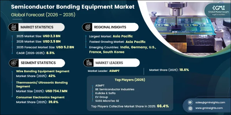
這項成長主要得益於全球晶圓廠產能的提升、7奈米以上先進製程節點的快速普及,以及對異構整合和先進封裝架構日益成長的需求。人工智慧、高效能運算和資料中心晶片生產的強勁投資勢頭持續推動著半導體前端和後端流程的設備需求。同時,政府主導的半導體本土化計畫正在重塑區域供應鏈,促進國內製造業的擴張,並降低對海外生產基地的依賴。向3D整合和晶片級設計的轉變也推動了對高精度鍵合技術的需求成長。整個製造生態系中的封裝技術日益複雜,對互連密度、散熱性能和電氣效率提出了更高的要求。所有這些都直接推動了邏輯、記憶體和特殊半導體應用領域對先進鍵合設備解決方案的需求。
| 市場範圍 | |
|---|---|
| 開始年份 | 2025 |
| 預測期 | 2026-2035 |
| 初始市場規模 | 23億美元 |
| 預測金額 | 52億美元 |
| 複合年成長率 | 8.5% |
預計到2025年,焊線設備市佔率將達到42%。其強勁的市場地位得益於其在高產量生產環境中的廣泛應用,在這些環境中,成本效益、產能和成熟製程的可靠性仍然至關重要。這項技術持續廣泛應用於汽車電子、消費性電子、LED模組、功率元件和類比積體電路等眾多領域。其對多種封裝形式的適應性確保了其持續的重要性,即使在新的互連技術不斷湧現的情況下,尤其是在需要可擴展且經濟高效的組裝解決方案的配置中,其重要性依然不減。
預計到2035年,混合鍵合產業將以21.3%的複合年成長率成長。其快速普及得益於3D整合和先進異構封裝技術的日益普及。直接銅對銅佈線技術正被廣泛採用,以實現更高的佈線密度、更優異的電氣性能和更小的尺寸。這些優勢使得混合鍵合成為實現下一代半導體架構的關鍵手段,而這些架構對極緻小型化和效能最佳化提出了更高的要求。
預計到2025年,北美半導體鍵結設備市佔率將達到18.3%。該地區的成長主要得益於大規模半導體產業回流計畫以及政府主導的旨在擴大國內封裝和組裝能力的投資。支持先進封裝技術開發的公共資金項目,在晶圓製造週期之外,也催生了對鍵合設備的額外需求,推動了全部區域長期裝置的成長。
競爭格局包括 Kulicke & Soffa、BE Semiconductor Industries、Shinkawa Ltd、Fasford Technology Co., Ltd、Hesse GmbH、F & K Delvotec Bondtechnik GmbH、KAIJO Corporation、Athlete FA Corporation、Micro Point Pro、F&S Bondintec Semiconductor GmbH、AConnPT、EVP . Co., Ltd. 和 Shibuya Corporation。半導體鍵合設備市場的企業正透過專注於滿足先進節點小型化和異質整合需求的下一代封裝解決方案來鞏固其市場地位。製造商正在加大對混合鍵合和 3D 鍵合技術的投資,以滿足對基於晶片組架構和高密度互連解決方案日益成長的需求。與半導體代工廠和 OSAT 供應商建立策略合作夥伴關係也是優先事項,以確保獲得長期的設備安裝合約和聯合開發項目。
目錄
第1章:調查方法和範圍
第2章執行摘要
第3章 行業洞察
- 產業生態系分析
- 供應商情況
- 利潤率
- 成本結構
- 每個階段增加的價值
- 影響價值鏈的因素
- 中斷
- 影響產業的因素
- 促進因素
- 擴大全球半導體製造能力並建造新工廠
- 過渡到7奈米以下的先進製程節點,並採用EUV光刻技術進行製造。
- 先進封裝和異質整合技術的廣泛應用
- 半導體製造在地化進程及政府主導的獎勵
- 高效能運算、人工智慧和資料中心晶片的生產成長。
- 產業潛在風險與挑戰
- 半導體製造設備屬於高資本密集和長投資回收期產業。
- 供應鏈中斷和對關鍵子部件的依賴
- 市場機遇
- 擴大半導體設備翻新與升級服務
- 半導體製造業在新興區域基地的擴張
- 促進因素
- 成長潛力分析
- 監理情勢
- 波特的分析
- PESTLE分析
- 技術與創新展望
- 最新科技趨勢
- 新興技術
- 價格趨勢
- 按地區
- 依產品
- 定價策略
- 新興經營模式
- 合規要求
- 專利和智慧財產權分析
第4章 競爭情勢
- 介紹
- 企業市佔率分析
- 按地區
- 市場集中度分析
- 主要公司的競爭標竿分析
- 財務績效比較
- 收入
- 利潤率
- R&D
- 產品系列比較
- 產品線寬度
- 科技
- 創新
- 區域擴張比較
- 全球擴張分析
- 服務網路覆蓋
- 按地區分類的市場滲透率
- 競爭定位矩陣
- 領導者
- 挑戰者
- 追蹤者
- 小眾玩家
- 戰略展望矩陣
- 財務績效比較
- 主要進展
- 併購
- 夥伴關係和聯盟
- 技術進步
- 擴張和投資策略
- 數位轉型計劃
- 新興企業競爭公司和新創企業的發展趨勢
第5章 市場估算與預測:依設備類型分類,2022-2035年
- 焊線設備
- 晶片黏合設備
- 傳統晶片鍵合機
- 覆晶合機
- 用於先進封裝的晶片鍵合機
- 取放/模具取放裝置
- 晶圓鍵合技術設備
- 混合鍵合設備
- 其他
- 透過鍵合技術
- 熱壓黏合
- 熱聲/超音波鍵合
- 共晶/焊料鍵合
- 黏合劑
- 熔合
- 陽極鍵合
- 混合鍵合
- 其他
- 透過使用
- 邏輯裝置
- 儲存裝置
- DRAM
- NAND快閃記憶體
- 高頻寬體(HBM)
- 半導體鍵合設備
- MEMS元件
- CMOS影像感測器(CIS)
- 射頻和微波設備
- 光電和光電子學
- 先進感測器設備
- 其他
- 產業最終用途
- 家用電子產品
- 車
- 資料中心和高效能運算 (HPC)
- 電訊
- 工業自動化
- 醫療保健和生命科學
- 航太/國防
- 其他
第6章 市場估算與預測:依黏合技術分類,2022-2035年
- 熱壓黏接
- 熱超音波/超音波粘合
- 共晶/焊料鍵合
- 黏合劑
- 熔合
- 陽極鍵合
- 混合鍵合
- 其他
第7章 市場估計與預測:依應用領域分類,2022-2035年
- 邏輯裝置
- 儲存裝置
- DRAM
- NAND快閃記憶體
- 高頻寬體(HBM)
- 半導體鍵合設備
- MEMS元件
- CMOS影像感測器(CIS)
- 射頻和微波設備
- 光電和光電子學
- 先進感測器設備
- 其他
第8章 市場估算與預測:依最終用途產業分類,2022-2035年
- 家用電子產品
- 車
- 資料中心和高效能運算 (HPC)
- 電訊
- 工業自動化
- 醫療保健和生命科學
- 航太/國防
- 其他
第9章 市場估計與預測:依地區分類,2022-2035年
- 北美洲
- 美國
- 加拿大
- 歐洲
- 德國
- 英國
- 法國
- 西班牙
- 義大利
- 俄羅斯
- 亞太地區
- 中國
- 印度
- 日本
- 澳洲
- 韓國
- 拉丁美洲
- 巴西
- 墨西哥
- 阿根廷
- 中東和非洲
- 南非
- 沙烏地阿拉伯
- UAE
第10章:公司簡介
- 全球主要公司
- ASMPT
- BE Semiconductor Industries
- Kulicke & Soffa
- EV Group
- SUSS MicroTec SE
- 該地區的主要公司
- 北美洲
- Micro Point Pro(MPP)Ltd
- 亞太地區
- Shinkawa Ltd
- Fasford Technology Co., Ltd
- KAIJO Corporation
- Athlete FA Corporation
- Panasonic Connect Co., Ltd
- Canon Machinery Inc
- Toray Engineering Co., Ltd
- Shibuya Corporation
- 歐洲
- Hesse GmbH
- F&K Delvotec Bondtechnik GmbH
- F&S Bondtec Semiconductor GmbH
- 北美洲
The Global Semiconductor Bonding Equipment Market was valued at USD 2.3 billion in 2025 and is estimated to grow at a CAGR of 8.5% to reach USD 5.2 billion by 2035.
Growth is supported by rising global fab capacity additions, rapid adoption of advanced nodes below 7nm, and increasing demand for heterogeneous integration and advanced packaging architectures. Strong investment momentum from artificial intelligence, high-performance computing, and data center chip production continues to reinforce equipment demand across front-end and back-end semiconductor processes. In parallel, government-led semiconductor localization programs are reshaping regional supply chains, encouraging domestic manufacturing expansion and reducing reliance on offshore production hubs. The ongoing transition toward 3D integration and chiplet-based designs is also intensifying the need for high-precision bonding technologies. Across fabrication ecosystems, packaging sophistication is increasing, requiring tighter interconnect density, improved thermal performance, and higher electrical efficiency, all of which directly elevate demand for advanced bonding equipment solutions across logic, memory, and specialty semiconductor applications.
| Market Scope | |
|---|---|
| Start Year | 2025 |
| Forecast Year | 2026-2035 |
| Start Value | $2.3 Billion |
| Forecast Value | $5.2 Billion |
| CAGR | 8.5% |
The wire bonding equipment segment accounted for 42% share in 2025. Its strong position is supported by extensive use in high-volume production environments where cost efficiency, throughput, and mature process reliability remain critical. This technology continues to be widely used in applications across automotive electronics, consumer devices, LED modules, power devices, and analog integrated circuits. Its adaptability across multiple packaging formats ensures continued relevance even as newer interconnect technologies emerge, particularly in configurations requiring scalable and cost-effective assembly solutions.
The hybrid bonding segment is expected to grow at a CAGR of 21.3% through 2035. Its rapid adoption is driven by the growing shift toward 3D integration and advanced heterogeneous packaging approaches. Copper-to-copper direct interconnection techniques are increasingly being adopted to achieve higher interconnect density, improved electrical performance, and reduced form factor. These capabilities are making hybrid bonding a key enabler for next-generation semiconductor architectures that require extreme miniaturization and performance optimization.
North America Semiconductor Bonding Equipment Market held 18.3% share in 2025. Regional growth is strongly influenced by large-scale semiconductor reshoring initiatives and government-backed investments aimed at expanding domestic packaging and assembly capabilities. Public funding programs supporting advanced packaging development are creating incremental demand for bonding equipment independent of wafer fabrication cycles, strengthening long-term installed base growth across the region.
The competitive landscape includes key industry participants such as Kulicke & Soffa, BE Semiconductor Industries, Shinkawa Ltd, Fasford Technology Co., Ltd, Hesse GmbH, F&K Delvotec Bondtechnik GmbH, KAIJO Corporation, Athlete FA Corporation, Micro Point Pro, F&S Bondtec Semiconductor GmbH, ASMPT, EV Group, SUSS MicroTec SE, Panasonic Connect Co., Ltd, Canon Machinery Inc, Toray Engineering Co., Ltd, and Shibuya Corporation. Companies in the semiconductor bonding equipment market are strengthening their market position by focusing on next-generation packaging solutions that support advanced node scaling and heterogeneous integration requirements. Manufacturers are increasing investment in hybrid and 3D bonding technologies to address rising demand for chiplet-based architectures and high-density interconnect solutions. Strategic collaborations with semiconductor foundries and OSAT providers are being prioritized to secure long-term equipment deployment contracts and co-development programs.
Table of Contents
Chapter 1 Methodology and Scope
- 1.1 Market scope and definition
- 1.2 Research design
- 1.2.1 Research approach
- 1.2.2 Data collection methods
- 1.3 Data mining sources
- 1.3.1 Global
- 1.3.2 Regional/Country
- 1.4 Base estimates and calculations
- 1.4.1 Base year calculation
- 1.4.2 Key trends for market estimation
- 1.5 Primary research and validation
- 1.5.1 Primary sources
- 1.6 Forecast model
- 1.7 Research assumptions and limitations
Chapter 2 Executive Summary
- 2.1 Industry 360° synopsis, 2022 - 2035
- 2.2 Key market trends
- 2.2.1 Equipment type trends
- 2.2.2 Bonding technology trends
- 2.2.3 Application trends
- 2.2.4 End-use industry trends
- 2.2.5 Regional trends
- 2.3 TAM Analysis, 2026-2035
- 2.4 CXO perspectives: Strategic imperatives
Chapter 3 Industry Insights
- 3.1 Industry ecosystem analysis
- 3.1.1 Supplier Landscape
- 3.1.2 Profit Margin
- 3.1.3 Cost structure
- 3.1.4 Value addition at each stage
- 3.1.5 Factor affecting the value chain
- 3.1.6 Disruptions
- 3.2 Industry impact forces
- 3.2.1 Growth drivers
- 3.2.1.1 Expansion of global semiconductor fabrication capacity and new fab construction
- 3.2.1.2 Transition to advanced process nodes below 7nm and EUV-based manufacturing
- 3.2.1.3 Rising adoption of advanced packaging and heterogeneous integration
- 3.2.1.4 Increasing semiconductor manufacturing localization and government-backed incentives
- 3.2.1.5 Growth in high-performance computing, AI, and data center chip production
- 3.2.2 Industry pitfalls and challenges
- 3.2.2.1 High capital intensity and long payback cycles of semiconductor equipment
- 3.2.2.2 Supply chain disruptions and dependence on critical sub-components
- 3.2.3 Market opportunities
- 3.2.3.1 Rising adoption of semiconductor equipment refurbishment and upgrade services
- 3.2.3.2 Expansion of semiconductor manufacturing in emerging regional hubs
- 3.2.1 Growth drivers
- 3.3 Growth potential analysis
- 3.4 Regulatory landscape
- 3.4.1 North America
- 3.4.2 Europe
- 3.4.3 Asia Pacific
- 3.4.4 Latin America
- 3.4.5 Middle East & Africa
- 3.5 Porter's analysis
- 3.6 PESTEL analysis
- 3.7 Technology and Innovation landscape
- 3.7.1 Current technological trends
- 3.7.2 Emerging technologies
- 3.8 Price trends
- 3.8.1 By region
- 3.8.2 By product
- 3.9 Pricing Strategies
- 3.10 Emerging Business Models
- 3.11 Compliance Requirements
- 3.12 Patent and IP analysis
Chapter 4 Competitive Landscape, 2025
- 4.1 Introduction
- 4.2 Company market share analysis
- 4.2.1 By region
- 4.2.1.1 North America
- 4.2.1.2 Europe
- 4.2.1.3 Asia Pacific
- 4.2.1.4 Latin America
- 4.2.1.5 Middle East & Africa
- 4.2.2 Market concentration analysis
- 4.2.1 By region
- 4.3 Competitive benchmarking of key players
- 4.3.1 Financial performance comparison
- 4.3.1.1 Revenue
- 4.3.1.2 Profit margin
- 4.3.1.3 R&D
- 4.3.2 Product portfolio comparison
- 4.3.2.1 Product range breadth
- 4.3.2.2 Technology
- 4.3.2.3 Innovation
- 4.3.3 Geographic presence comparison
- 4.3.3.1 Global footprint analysis
- 4.3.3.2 Service network coverage
- 4.3.3.3 Market penetration by region
- 4.3.4 Competitive positioning matrix
- 4.3.4.1 Leaders
- 4.3.4.2 Challengers
- 4.3.4.3 Followers
- 4.3.4.4 Niche players
- 4.3.5 Strategic outlook matrix
- 4.3.1 Financial performance comparison
- 4.4 Key developments
- 4.4.1 Mergers and acquisitions
- 4.4.2 Partnerships and collaborations
- 4.4.3 Technological advancements
- 4.4.4 Expansion and investment strategies
- 4.4.5 Digital transformation initiatives
- 4.5 Emerging/ startup competitors landscape
Chapter 5 Market Estimates and Forecast, By Equipment Type, 2022 - 2035 (USD Million)
- 5.1 Key trends
- 5.2 Wire bonding equipment
- 5.3 Die bonding equipment
- 5.3.1 Conventional die bonders
- 5.3.2 Flip-chip bonders
- 5.3.3 Advanced packaging die bonders
- 5.3.4 Pick-and-place / Die-picking equipment
- 5.4 Wafer bonding equipment
- 5.5 Hybrid bonding equipment
- 5.6 Others
- 5.7 By Bonding Technology
- 5.8 Thermocompression bonding
- 5.9 Thermosonic / ultrasonic bonding
- 5.10 Eutectic / solder bonding
- 5.11 Adhesive bonding
- 5.12 Fusion bonding
- 5.13 Anodic bonding
- 5.14 Hybrid bonding
- 5.15 Others
- 5.16 By Application
- 5.17 Logic devices
- 5.18 Memory devices
- 5.19 DRAM
- 5.20 NAND flash
- 5.21 High-bandwidth memory (HBM)
- 5.22 Semiconductor bonding equipments
- 5.23 MEMS devices
- 5.24 CMOS image sensors (CIS)
- 5.25 RF & microwave devices
- 5.26 Photonics & optoelectronics
- 5.27 Advanced sensor devices
- 5.28 Others
- 5.29 By End-Use Industry
- 5.30 Consumer electronics
- 5.31 Automotive
- 5.32 Data centers & high-performance computing (HPC)
- 5.33 Telecommunications
- 5.34 Industrial & automation
- 5.35 Healthcare & life sciences
- 5.36 Aerospace & defense
- 5.37 Others
Chapter 6 Market Estimates and Forecast, By Bonding Technology, 2022 - 2035 (USD Million)
- 6.1 Key trends
- 6.2 Thermocompression bonding
- 6.3 Thermosonic / ultrasonic bonding
- 6.4 Eutectic / solder bonding
- 6.5 Adhesive bonding
- 6.6 Fusion bonding
- 6.7 Anodic bonding
- 6.8 Hybrid bonding
- 6.9 Others
Chapter 7 Market Estimates and Forecast, By Application, 2022 - 2035 (USD Million)
- 7.1 Key trends
- 7.2 Logic devices
- 7.3 Memory devices
- 7.3.1 DRAM
- 7.3.2 NAND flash
- 7.3.3 High-bandwidth memory (HBM)
- 7.4 Semiconductor bonding equipments
- 7.5 MEMS devices
- 7.6 CMOS image sensors (CIS)
- 7.7 RF & microwave devices
- 7.8 Photonics & optoelectronics
- 7.9 Advanced sensor devices
- 7.10 Others
Chapter 8 Market Estimates and Forecast, By End-Use Industry, 2022 - 2035 (USD Million)
- 8.1 Key trends
- 8.2 Consumer electronics
- 8.3 Automotive
- 8.4 Data centers & high-performance computing (HPC)
- 8.5 Telecommunications
- 8.6 Industrial & automation
- 8.7 Healthcare & life sciences
- 8.8 Aerospace & defense
- 8.9 Others
Chapter 9 Market Estimates and Forecast, By Region, 2022 - 2035 (USD Million)
- 9.1 Key trends
- 9.2 North America
- 9.2.1 U.S.
- 9.2.2 Canada
- 9.3 Europe
- 9.3.1 Germany
- 9.3.2 UK
- 9.3.3 France
- 9.3.4 Spain
- 9.3.5 Italy
- 9.3.6 Russia
- 9.4 Asia Pacific
- 9.4.1 China
- 9.4.2 India
- 9.4.3 Japan
- 9.4.4 Australia
- 9.4.5 South Korea
- 9.5 Latin America
- 9.5.1 Brazil
- 9.5.2 Mexico
- 9.5.3 Argentina
- 9.6 Middle East and Africa
- 9.6.1 South Africa
- 9.6.2 Saudi Arabia
- 9.6.3 UAE
Chapter 10 Company Profiles
- 10.1 Global Key Players
- 10.1.1 ASMPT
- 10.1.2 BE Semiconductor Industries
- 10.1.3 Kulicke & Soffa
- 10.1.4 EV Group
- 10.1.5 SUSS MicroTec SE
- 10.2 Regional key players
- 10.2.1 North America
- 10.2.1.1 Micro Point Pro (MPP) Ltd
- 10.2.2 Asia Pacific
- 10.2.2.1 Shinkawa Ltd
- 10.2.2.2 Fasford Technology Co., Ltd
- 10.2.2.3 KAIJO Corporation
- 10.2.2.4 Athlete FA Corporation
- 10.2.2.5 Panasonic Connect Co., Ltd
- 10.2.2.6 Canon Machinery Inc
- 10.2.2.7 Toray Engineering Co., Ltd
- 10.2.2.8 Shibuya Corporation
- 10.2.3 Europe
- 10.2.3.1 Hesse GmbH
- 10.2.3.2 F&K Delvotec Bondtechnik GmbH
- 10.2.3.3 F&S Bondtec Semiconductor GmbH
- 10.2.1 North America

 半導體鍵結:市場佔有率分析、產業趨勢與統計、成長預測(2026-2031)
 半導體晶圓鍵合技術市場分析及預測至 2035 年:按類型、產品類型、技術、應用、材料類型、製程、最終用戶、設備和解決方案分類。
 半導體鍵合市場:2026-2032年全球市場預測(依設備類型、鍵結方法、封裝結構、基板材料、應用、最終用戶和產業分類)半導體鍵結市場分析及預測(至2035年):類型、產品、技術、應用、材料類型、裝置、製程、最終用戶、設備、解決方案
 半導體鍵結市場規模、佔有率、成長及全球產業分析:依類型、應用和地區劃分的洞察與預測(2026-2034年)
 半導體鍵結市場-全球產業規模、佔有率、趨勢、機會與預測:按類型、製程類型、鍵結技術、應用、地區和競爭格局分類,2021-2031年半導體鍵合設備:市場佔有率分析、產業趨勢與統計、成長預測(2026-2031)
 半導體鍵合市場,按鍵合技術、鍵結材料、最終用戶和地區分類
 全球混合鍵結市場按封裝架構、設備類型和整合度分類-預測至2032年
 TCB鍵合機:全球市佔率排名、總銷售額與需求預測(2025-2031年)