


 |
市場調查報告書
商品編碼
2099437
GPU晶片封裝:市佔率分析、產業趨勢與統計、成長預測(2026-2031年)GPU Chiplet Packaging - Market Share Analysis, Industry Trends & Statistics, Growth Forecasts (2026 - 2031) |
||||||

※ 本網頁內容可能與最新版本有所差異。詳細情況請與我們聯繫。
根據 Mordor Intelligence 預測,GPU 晶片封裝市場預計將從 2025 年的 76 億美元成長到 2026 年的 112 億美元,到 2031 年達到 298.9 億美元,2026 年至 2031 年的複合年成長率預計為 21.69%。
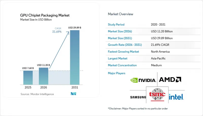
本報告按GPU平台(包括資料中心GPU和AI GPU)、封裝技術(包括2.5D中介層封裝和橋接封裝)、晶片功能(包括用於GPU運算的晶片)、應用(包括AI訓練和推理、雲端運算)、最終用戶(包括超大規模資料中心業者和雲端服務供應商)以及地區進行細分。市場預測以美元(USD)為單位。
全球GPU晶片封裝市場趨勢與洞察
配備 HBM 顯存的 AI GPU 封裝的需求不斷成長
超大規模資料中心業者資料中心營運商對人工智慧基礎設施的投資仍是GPU晶片封裝市場最明顯的短期需求推動要素。 NVIDIA資料中心部門累計,截至2026年4月的第一季營收為752億美元,年增92%。 2027會計年度第二季的預測營收為910億美元。草案指出,產品產量的增加與封裝的複雜性直接相關,因為每個Blackwell B200封裝都將兩個運算晶片和八個HBM3E堆疊整合在CoWoS-L基板上。這種配置使得每筆新的AI GPU訂單都直接需要先進的封裝生產線、先進的基板以及高密度記憶體整合。因此,GPU晶片封裝市場不再主要受半導體週期影響,而是更取決於大規模加速器部署的時機。這也解釋了為什麼封裝能力已成為策略性瓶頸,而不僅僅是日常的後端製造流程。
資料中心效能擴展的異質整合
由於僅靠簡單的製程小型化已不足以在系統級性能上與最先進的加速器相媲美,異質整合已成為提升性能的核心手段。據英特爾稱,Foveros Direct 3D 透過直接銅對銅鍵合實現了小於 10µm 的互連間距,互連密度比傳統的微凸塊方法高出 10 倍。這種高密度支援晶片的垂直堆疊佈局,而這種佈局對於需要在極窄的物理距離內運行的計算、記憶體和 I/O 功能至關重要。此架構的邏輯不僅限於旗艦 GPU,還延伸至超大規模超大規模資料中心業者團隊設計的客製化 AI 推理晶片程式。這擴大了 GPU 晶片封裝市場的潛在需求範圍,使其超越了標準 GPU 供應商的藍圖。同時,這也凸顯了能夠同時考慮並解決設計、散熱和組裝限制的封裝團隊的重要性。
包裝成本高且大規模生產能力有限
高昂的封裝成本持續限制尖端配置的應用,使其僅限於高附加價值計算項目。根據草案,與更簡單的CoWoS-S設計相比,用於當前一代AI GPU的CoWoS-L封裝需要額外的局部矽橋接元件、更多的微凸塊以及更低的初始組裝良率。這種成本差異意義重大,因為推動市場成長的客戶掌握著大部分可用的認證產能。供應問題不僅限於組裝流程;為了順利實現商業化生產並擴大規模,基板、特殊材料和鍵合設備都需要協同工作。此外,每種新的封裝都需要GPU、HBM和基板供應商之間進行協調的認證流程,才能實現收入規模化成長。因此,GPU晶片封裝市場面臨結構性錯配:需求前景光明,但供應鏈卻落後。
細分市場分析
截至2025年,資料中心和人工智慧領域的GPU將佔據GPU晶片封裝市場佔有率的86.11%,預計到2031年將以23.21%的複合年成長率成長。這種市場集中度反映出,超大規模資料中心業者和企業級人工智慧專案訂購的是封裝複雜度最高的裝置,而非銷量最高的裝置。這些平台需要採用CoWoS-L、先進有機基板覆晶或3D整合技術,因此其單晶片封裝價值遠高於面向客戶端的標準圖形產品。 NVIDIA 2027年第一季資料中心業務營收達752億美元,顯示該領域的需求強勁。因此,GPU晶片封裝市場的發展主要由那些兼具最高記憶體頻寬需求和最高封裝複雜性的平台類型所驅動。
高效能運算 (HPC) GPU 是本次草案中第二大平台,仍服務於需要高效能 2.5D 封裝的科學運算、氣候建模和國防工作負載。雖然其出貨量小於 AI 加速器,但對性能和可靠性的要求仍然很高。專業和工作站 GPU 佔據中階市場,在這個市場中,先進的有機基板解決方案比全矽中介層整合更為常見。客戶端和遊戲 GPU 的出貨量仍然很大,但由於其封裝密度和記憶體使用量較低,導致先進封裝帶來的單晶片收益較低。隨著 AI 加速器朝向更大的封裝尺寸和更多的 HBM 堆疊發展,出貨量和封裝價值之間的差距正在擴大。這種差距的擴大進一步鞏固了資料中心 GPU 在 GPU 晶片封裝市場的高階地位。
到2025年,基於2.5D中介層和橋接技術的封裝將佔據GPU晶片封裝市場68.33%的佔有率,而3D堆疊和混合鍵合封裝預計到2031年將以23.62%的複合年成長率成長。 2.5D封裝目前的主導地位反映了市場上現有AI加速器成熟的製造基礎設施。台積電的CoWoS系列和英特爾的EMIB平台已建立成熟的生產基地,其大規模生產供應和封裝可靠性已獲得現有客戶的信賴。英特爾也將Foveros Direct 3D定位為新一代更精確的直接接合和高密度垂直整合方案。這意味著,儘管3D技術的戰略重要性日益凸顯,但GPU晶片封裝市場仍主要依靠2.5D封裝的銷售來支撐。
根據這份草案,未來的記憶體和邏輯設計將需要極其精細的互連幾何結構,傳統的微凸塊製程無法滿足這項需求,進而推動了3D堆疊和混合鍵結技術的發展。扇出型和基於RDL的封裝為那些需要高整合度但又不想承擔矽中介層方法全部成本的客戶提供了一種替代方案。基於有機基板的多晶片封裝在頻寬密度和熱負載相對較低的客戶端GPU和入門級工作站應用中仍然發揮著重要作用。此外,隨著高頻寬記憶體介面和晶片間連接必須在更嚴格的電氣和熱限制下進行認證,符合標準變得越來越重要。因此,製程成熟度(而不僅僅是創新性)將成為商業性應用的關鍵因素。因此,GPU晶片封裝市場預計將分階段發展,2.5D封裝仍將在量產中佔據主導地位,而3D封裝最初將在高價值項目中擴展。
區域分析
到2025年,亞太地區將佔據GPU晶片封裝市場88.44%的佔有率,這反映出該地區晶圓代工廠、OSAT廠商、基板供應商和記憶體製造商的高度集中。台灣憑藉台積電的先進封裝設施和日月光科技在半導體組裝測試(OSAT)業務方面的規模優勢,在該生態系統中扮演關鍵角色。台灣的優勢不僅在於其產能,還在於其供應鏈的接近性,涵蓋封裝材料、基板和工程人才。韓國憑藉其在HBM記憶體領域的領先地位以及整合相關封裝的能力,鞏固了其在該地區的地位,而封裝對於人工智慧加速器仍然至關重要。日本也保持著重要的戰略地位,因為日本本土供應商生產的ABF基板是整個封裝產業鏈中的重要瓶頸。
預計到2031年,北美將以23.42%的複合年成長率成長,成為GPU晶片封裝市場成長最快的區域叢集。根據美國國會研究服務處(CRS)報告顯示,《晶片與科學法案》正在為國內製造和封裝產業建立更強大的投資基礎,公共和獎勵總額達467億美元。安靠(Amkor)位於亞利桑那州的先進封裝園區和格羅方德(GlobalFoundries)位於紐約的先進封裝與光電中心是這些政策支持的擴張中最突出的例證。格羅方德表示,其紐約中心於2025年1月開業,投資額達5.75億美元,其中7,500萬美元直接來自《晶片與科學法案》。該地區強勁的成長並非源自於其運作即將超越亞太地區,而是因為其起步基數較低。
儘管歐洲在GPU晶片封裝市場的商業性佔有率不大,但在3D整合和異構封裝的研究領域仍舉足輕重。該地區的重要性更源自於imec、弗勞恩霍夫研究所和CEA-Leti等機構的研發投入,而非大規模量產。南美、中東和非洲的需求仍處於起步階段,目前缺乏足夠先進的封裝製造地。中東正透過政府的人工智慧投資計畫崛起為需求中心,而非洲的角色則主要依賴更大規模資料中心的建設和進口加速器的供應。
其他好處:
- Excel格式的市場預測(ME)表
- 3個月的分析師支持
目錄
第1章:引言
- 研究假設和市場定義
- 調查範圍
第2章:調查方法
第3章執行摘要
第4章 市場狀況
- 市場概覽
- 市場促進因素
- 配備 HBM 顯存的 AI GPU 封裝的需求不斷成長
- 與單晶片相比,小型GPU晶片具有良率優勢
- 異質整合以擴展資料中心效能
- 彈性供應鏈:向基於晶片的設計復用轉型
- 晶圓代工廠及OSAT廠商對先進封裝生產能力的投資
- GPU藍圖需要多晶片散熱和功耗最佳化
- 市場限制因素
- 包裝成本高且大規模生產能力不足
- 高密度佈線中熱完整性和訊號完整性的複雜性。
- 圍繞專有包裝平台的生態系統鎖定
- GPU、記憶體和基板供應商的認證風險
- 產業價值鏈分析
- 原料和基礎材料
- 設計與智慧財產權(IP)開發
- 晶圓製造
- 組裝和先進包裝
- 測試與檢驗
- 按最終用戶分類的部署狀態
- 監理情勢
- 技術展望
- 2.5D中介層和橋接封裝
- 3D堆疊和混合黏合包裝
- 扇出型和基於 RDL 的封裝
- 整合式高頻寬記憶體
- 溫度控管和協同設計
- 波特五力分析
- 價格分析
- 宏觀經濟因素對市場的影響
第5章 市場規模與成長預測
- 透過GPU平台
- 用於資料中心和人工智慧的GPU
- 用於高效能運算的GPU
- 專業級與工作站級GPU
- 客戶端和遊戲 GPU
- 其他GPU平台
- 生產力
- 2.5D中介層和橋接封裝
- 3D堆疊和混合黏合包裝
- 扇出型和基於 RDL 的封裝
- 採用有機基板的多晶片封裝
- 其他包裝技術
- 晶片組按功能
- GPU運算晶片
- 記憶體晶片
- I/O 和基片晶片
- 用於連接和介面的晶片
- 其他晶片組
- 透過使用
- 人工智慧訓練和推理
- 高效能運算
- 雲端運算
- 商用視覺化
- 遊戲和消費圖形
- 其他用途
- 最終用戶
- 超大規模資料中心業者和雲端服務供應商
- 企業資料中心
- 研究機構及政府附屬高效能運算中心
- 原始設備製造商和系統整合商
- 其他最終用戶
- 按地區
- 北美洲
- 美國
- 加拿大
- 墨西哥
- 歐洲
- 德國
- 英國
- 法國
- 義大利
- 其他歐洲國家
- 亞太地區
- 中國
- 日本
- 韓國
- 印度
- 東南亞
- 其他亞太國家
- 南美洲
- 中東
- 非洲
- 北美洲
第6章 競爭情勢
- 市場集中度
- 策略趨勢
- 市佔率分析
- 公司簡介
- NVIDIA Corporation
- Advanced Micro Devices, Inc.
- Taiwan Semiconductor Manufacturing Company Limited
- Intel Corporation
- Samsung Electronics Co., Ltd.
- SK hynix Inc.
- Micron Technology, Inc.
- Amkor Technology, Inc.
- ASE Technology Holding Co., Ltd.
- JCET Group Co., Ltd.
- Tongfu Microelectronics Co., Ltd.
- SPIL, Siliconware Precision Industries Co., Ltd.
- Powertech Technology Inc.
- Unimicron Technology Corporation
- Shinko Electric Industries Co., Ltd.
- Murata Manufacturing Co., Ltd.
- Ibiden Co., Ltd.
- Kyocera Corporation
- ASE Group
- TSMC
- GlobalFoundries Inc.
第7章 市場機會與未來展望
According to Mordor Intelligence, the GPU chiplet packaging market size is expected to increase from USD 7.60 billion in 2025 to USD 11.20 billion in 2026 and reach USD 29.89 billion by 2031, growing at a CAGR of 21.69% over 2026-2031.
This report is Segmented by GPU Platform (Data Center and AI GPUs, and More), Packaging Technology (2. 5D Interposer and Bridge-Based Packaging, and More), Chiplet Function (GPU Compute Chiplets, and More), Application (AI Training and Inference, Cloud Computing, and More), End User (Hyperscalers and Cloud Providers, and More), and Geography. The Market Forecasts are Provided in Terms of Value (USD).
Global GPU Chiplet Packaging Market Trends and Insights
Rising AI GPU Demand for HBM-Attached Packages
Hyperscaler AI infrastructure spending remains the clearest near-term demand driver for the GPU chiplet packaging market. NVIDIA's data center segment generated USD 75.2 billion in Q1 FY2027, the quarter ending April 2026, and this was 92% higher than the prior year, while Q2 FY2027 guidance was set at USD 91.0 billion. The draft links that product ramp directly to package complexity, because each Blackwell B200 package combines 2 compute dies with 8 HBM3E stacks on a CoWoS-L substrate. That configuration means each new AI GPU order translates into direct demand for advanced packaging lines, advanced substrates, and high-density memory integration. The result is that the GPU chiplet packaging market is no longer being shaped mainly by broad semiconductor cycles, but by the timing of very large accelerator deployments. This also explains why packaging capacity has become a strategic bottleneck rather than a routine back-end manufacturing step.
Heterogeneous Integration for Datacenter Performance Scaling
Heterogeneous integration has become a core performance lever because simple process shrinks no longer deliver enough system-level gain for leading accelerators. Intel stated that Foveros Direct 3D achieves sub-10 µm interconnect pitch through direct copper-to-copper bonding and can provide up to 10x finer interconnect density than conventional microbump approaches. That level of density supports the vertical die-stacking layouts needed when compute, memory, and I/O functions must operate within a very small physical distance. The same architectural logic is moving beyond flagship GPUs and into custom AI inference silicon programs designed by hyperscaler teams. This broadens the addressable volume base for the GPU chiplet packaging market beyond the standard GPU vendor roadmap. It also raises the importance of packaging teams that can work across design, thermal, and assembly constraints at the same time.
High Packaging Cost and Limited High-Volume Capacity
High package cost still limits the broad adoption of leading-edge configurations to the highest-value compute programs. The draft states that CoWoS-L packaging for current-generation AI GPUs requires added local silicon bridge elements, higher microbump counts, and lower early-stage assembly yields than simpler CoWoS-S designs. That cost difference matters because the same customers driving market growth are also reserving much of the available qualified capacity. The supply issue is wider than assembly alone, since substrates, specialty materials, and bonding tools all have to scale together for commercial output to increase smoothly. Each new package also needs coordinated qualification across GPU, HBM, and substrate suppliers before revenue can ramp. As a result, the GPU chiplet packaging market faces a structural mismatch between strong demand visibility and slower supply readiness.
Other drivers and restraints analyzed in the detailed report include:
- Yield Advantage of Smaller GPU Chiplets Versus Monolithic Dies
- Advanced Packaging Capacity Investments by Foundries and OSATs
- Thermal and Signal Integrity Complexity in Dense Interconnects
For complete list of drivers and restraints, kindly check the Table Of Contents.
Segment Analysis
Data Center and AI GPUs held 86.11% of GPU chiplet packaging market share in 2025 and are projected to expand at a 23.21% CAGR through 2031. This concentration reflects the fact that hyperscalers and enterprise AI programs are ordering the most packaging-intensive devices, not the highest historical unit-volume devices. These platforms require CoWoS-L, advanced organic substrate flip-chip, or 3D integration methods that carry far more packaging value per chip than standard client graphics products. NVIDIA's data center segment revenue of USD 75.2 billion in Q1 FY2027 provides a current-year anchor for the demand intensity behind this category. The GPU chiplet packaging market is therefore being led by the platform class that combines the greatest memory bandwidth needs with the greatest package complexity.
HPC GPUs form the second-largest platform in the draft and serve scientific computing, climate modeling, and defense workloads that still require highly capable 2.5D packaging. Their volumes are lower than the AI accelerator class, but their performance and reliability needs remain demanding. Professional and workstation GPUs sit in a middle tier, where advanced organic substrate solutions are more common than full silicon interposer integration. Client and gaming GPUs still represent a large unit base, but they produce less advanced packaging revenue per chip because their package structures are less dense and less memory intensive. This gap between unit volume and packaging value is widening as AI accelerators move to larger package footprints and higher HBM stack counts. That widening gap reinforces the premium position of data center GPUs within the GPU chiplet packaging market.
2.5D Interposer and Bridge-Based Packaging accounted for 68.33% of GPU chiplet packaging market size in 2025, while 3D Stacked and Hybrid-Bonded Packaging is forecast to grow at a 23.62% CAGR through 2031. The present leadership of 2.5D formats reflects proven manufacturing readiness across current AI accelerators in commercial shipment. TSMC's CoWoS family and Intel's EMIB platform established a production base that current customers already trust for volume delivery and package reliability. Intel also positioned Foveros Direct 3D as a next-stage path for tighter direct bonding and denser vertical integration. This means the GPU chiplet packaging market is still anchored by 2.5D revenue even as 3D technologies gain strategic importance.
The draft shows that 3D stacked and hybrid-bonded formats are gaining momentum because future memory and logic designs need much finer interconnect geometry than conventional microbump flows can support. Fan-Out and RDL-based packaging provides an alternative path for customers that need advanced integration without the full cost profile of silicon interposer approaches. Organic substrate-based multi-die packaging remains relevant for client GPU and entry workstation programs where bandwidth density and thermal load are more moderate. Standards compliance is also becoming more important because high-bandwidth memory interfaces and die-to-die connections have to qualify within tighter electrical and thermal limits. This puts process maturity, not just novelty, at the center of commercial adoption. As a result, the GPU chiplet packaging market is likely to move in stages, with 2.5D staying dominant in volume while 3D expands first in the highest-value programs.
Complete Report Scope:
- By GPU Platform
- Data Center and AI GPUs
- HPC GPUs
- Professional and Workstation GPUs
- Client and Gaming GPUs
- Other GPU Platforms
- By Packaging Technology
- 2.5D Interposer and Bridge-Based Packaging
- 3D Stacked and Hybrid-Bonded Packaging
- Fan-Out and RDL-Based Packaging
- Organic Substrate-Based Multi-Die Packaging
- Other Packaging Technologies
- By Chiplet Function
- GPU Compute Chiplets
- Memory Chiplets
- I/O and Base Die Chiplets
- Connectivity and Interface Chiplets
- Other Chiplets
- By Application
- AI Training and Inference
- High-Performance Computing
- Cloud Computing
- Professional Visualization
- Gaming and Consumer Graphics
- Other Applications
- By End User
- Hyperscalers and Cloud Providers
- Enterprise Data Centers
- Research and Government HPC Centers
- OEMs and System Integrators
- Other End Users
- By Geography
- North America
- United States
- Canada
- Mexico
- Europe
- Germany
- United Kingdom
- France
- Italy
- Rest of Europe
- Asia-Pacific
- China
- Japan
- South Korea
- India
- Southeast Asia
- Rest of Asia-Pacific
- South America
- Middle East
- Africa
- North America
Geography Analysis
Asia-Pacific held 88.44% of the GPU chiplet packaging market share in 2025, which reflects the region's deep concentration of foundries, OSATs, substrate suppliers, and memory producers. Taiwan anchors this ecosystem through TSMC's advanced packaging base and ASE Technology Holding's scale in outsourced semiconductor assembly and test. Taiwan's advantage is not only production capacity, but also supply chain proximity across packaging materials, substrates, and engineering talent. South Korea supports the regional position through HBM memory leadership and related package integration capabilities that remain critical for AI accelerators. Japan also retains strategic relevance because ABF substrate production from local suppliers sits at a key chokepoint in the wider packaging chain.
North America is forecast to grow at a 23.42% CAGR through 2031, making it the fastest-growing regional cluster in the GPU chiplet packaging market. The CHIPS and Science Act created a stronger investment base for domestic manufacturing and packaging, with public and private incentives totaling USD 46.7 billion in the cited CRS report. Amkor's Arizona advanced packaging campus and GlobalFoundries' New York Advanced Packaging and Photonics Center are the clearest operating examples of that policy-backed buildout. GlobalFoundries said its New York center opened in January 2025 with USD 575 million in investment and USD 75 million in direct CHIPS Act support. The region's growth rate is strong because it is starting from a low base, not because it is close to displacing Asia-Pacific in current installed capacity.
Europe holds a modest commercial position in the GPU chiplet packaging market, but it remains important in 3D integration and heterogeneous packaging research. The region's relevance comes more from technology development at centers such as imec, Fraunhofer institutes, and CEA-Leti than from large qualified production volumes. South America, the Middle East, and Africa remain early-stage demand regions and do not yet have material leading-edge packaging manufacturing bases. The Middle East is emerging as a demand node through sovereign AI investment programs, while Africa's role remains tied to broader data center buildout and imported accelerator supply.
- NVIDIA Corporation
- Advanced Micro Devices, Inc.
- Taiwan Semiconductor Manufacturing Company Limited
- Intel Corporation
- Samsung Electronics Co., Ltd.
- SK hynix Inc.
- Micron Technology, Inc.
- Amkor Technology, Inc.
- ASE Technology Holding Co., Ltd.
- JCET Group Co., Ltd.
- Tongfu Microelectronics Co., Ltd.
- SPIL, Siliconware Precision Industries Co., Ltd.
- Powertech Technology Inc.
- Unimicron Technology Corporation
- Shinko Electric Industries Co., Ltd.
- Murata Manufacturing Co., Ltd.
- Ibiden Co., Ltd.
- Kyocera Corporation
- ASE Group
- TSMC
- GlobalFoundries Inc.
Additional Benefits:
- The market estimate (ME) sheet in Excel format
- 3 months of analyst support
TABLE OF CONTENTS
1 INTRODUCTION
- 1.1 Study Assumptions and Market Definition
- 1.2 Scope of the Study
2 RESEARCH METHODOLOGY
3 EXECUTIVE SUMMARY
4 MARKET LANDSCAPE
- 4.1 Market Overview
- 4.2 Market Drivers
- 4.2.1 Rising AI GPU Demand for HBM-Attached Packages
- 4.2.2 Yield Advantage of Smaller GPU Chiplets Versus Monolithic Dies
- 4.2.3 Heterogeneous Integration for Datacenter Performance Scaling
- 4.2.4 Resilient Supply Chain Shift Toward Chiplet-Based Design Reuse
- 4.2.5 Advanced Packaging Capacity Investments by Foundries and OSATs
- 4.2.6 GPU Roadmaps Requiring Multi-Die Thermal and Power Optimization
- 4.3 Market Restraints
- 4.3.1 High Packaging Cost and Limited High-Volume Capacity
- 4.3.2 Thermal and Signal Integrity Complexity in Dense Interconnects
- 4.3.3 Ecosystem Lock-In Around Proprietary Packaging Platforms
- 4.3.4 Qualification Risk Across GPU, Memory, and Substrate Suppliers
- 4.4 Industry Value Chain Analysis
- 4.4.1 Raw Materials and Substrates
- 4.4.2 Design and IP Development
- 4.4.3 Wafer Fabrication
- 4.4.4 Assembly and Advanced Packaging
- 4.4.5 Test and Validation
- 4.4.6 End-Use Deployment
- 4.5 Regulatory Landscape
- 4.6 Technological Outlook
- 4.6.1 2.5D Interposer and Bridge-Based Packaging
- 4.6.2 3D Stacked and Hybrid-Bonded Packaging
- 4.6.3 Fan-Out and RDL-Based Packaging
- 4.6.4 High Bandwidth Memory Integration
- 4.6.5 Thermal Management and Co-Design
- 4.7 Porter's Five Forces Analysis
- 4.7.1 Bargaining Power of Suppliers
- 4.7.2 Bargaining Power of Buyers
- 4.7.3 Threat of New Entrants
- 4.7.4 Threat of Substitutes
- 4.7.5 Intensity of Competitive Rivalry
- 4.8 Pricing Analysis
- 4.9 Impact of Macroeconomic Factors on the Market
5 MARKET SIZE AND GROWTH FORECASTS (VALUE)
- 5.1 By GPU Platform
- 5.1.1 Data Center and AI GPUs
- 5.1.2 HPC GPUs
- 5.1.3 Professional and Workstation GPUs
- 5.1.4 Client and Gaming GPUs
- 5.1.5 Other GPU Platforms
- 5.2 By Packaging Technology
- 5.2.1 2.5D Interposer and Bridge-Based Packaging
- 5.2.2 3D Stacked and Hybrid-Bonded Packaging
- 5.2.3 Fan-Out and RDL-Based Packaging
- 5.2.4 Organic Substrate-Based Multi-Die Packaging
- 5.2.5 Other Packaging Technologies
- 5.3 By Chiplet Function
- 5.3.1 GPU Compute Chiplets
- 5.3.2 Memory Chiplets
- 5.3.3 I/O and Base Die Chiplets
- 5.3.4 Connectivity and Interface Chiplets
- 5.3.5 Other Chiplets
- 5.4 By Application
- 5.4.1 AI Training and Inference
- 5.4.2 High-Performance Computing
- 5.4.3 Cloud Computing
- 5.4.4 Professional Visualization
- 5.4.5 Gaming and Consumer Graphics
- 5.4.6 Other Applications
- 5.5 By End User
- 5.5.1 Hyperscalers and Cloud Providers
- 5.5.2 Enterprise Data Centers
- 5.5.3 Research and Government HPC Centers
- 5.5.4 OEMs and System Integrators
- 5.5.5 Other End Users
- 5.6 By Geography
- 5.6.1 North America
- 5.6.1.1 United States
- 5.6.1.2 Canada
- 5.6.1.3 Mexico
- 5.6.2 Europe
- 5.6.2.1 Germany
- 5.6.2.2 United Kingdom
- 5.6.2.3 France
- 5.6.2.4 Italy
- 5.6.2.5 Rest of Europe
- 5.6.3 Asia-Pacific
- 5.6.3.1 China
- 5.6.3.2 Japan
- 5.6.3.3 South Korea
- 5.6.3.4 India
- 5.6.3.5 Southeast Asia
- 5.6.3.6 Rest of Asia-Pacific
- 5.6.4 South America
- 5.6.5 Middle East
- 5.6.6 Africa
- 5.6.1 North America
6 COMPETITIVE LANDSCAPE
- 6.1 Market Concentration
- 6.2 Strategic Moves
- 6.3 Market Share Analysis
- 6.4 Company Profiles (includes Global Level Overview, Market Level Overview, Core Segments, Financials as available, Strategic Information, Market Rank/Share, Products and Services, Recent Developments)
- 6.4.1 NVIDIA Corporation
- 6.4.2 Advanced Micro Devices, Inc.
- 6.4.3 Taiwan Semiconductor Manufacturing Company Limited
- 6.4.4 Intel Corporation
- 6.4.5 Samsung Electronics Co., Ltd.
- 6.4.6 SK hynix Inc.
- 6.4.7 Micron Technology, Inc.
- 6.4.8 Amkor Technology, Inc.
- 6.4.9 ASE Technology Holding Co., Ltd.
- 6.4.10 JCET Group Co., Ltd.
- 6.4.11 Tongfu Microelectronics Co., Ltd.
- 6.4.12 SPIL, Siliconware Precision Industries Co., Ltd.
- 6.4.13 Powertech Technology Inc.
- 6.4.14 Unimicron Technology Corporation
- 6.4.15 Shinko Electric Industries Co., Ltd.
- 6.4.16 Murata Manufacturing Co., Ltd.
- 6.4.17 Ibiden Co., Ltd.
- 6.4.18 Kyocera Corporation
- 6.4.19 ASE Group
- 6.4.20 TSMC
- 6.4.21 GlobalFoundries Inc.
7 MARKET OPPORTUNITIES AND FUTURE OUTLOOK
- 7.1 White-Space and Unmet-Need Assessment

 2026年全球先進封裝技術市場報告2026年全球先進半導體封裝市場報告
 下一代晶片和先進封裝架構:重新定義人工智慧和高效能運算的效能和可擴展性
 先進封裝:市場佔有率分析、產業趨勢與統計、成長預測(2026-2031)
 先進半導體封裝市場-2026-2032年全球市場預測
 全球先進半導體封裝市場:按技術、產品、應用和最終用戶分類-市場規模、產業動態、機會分析和預測(2026-2035 年)2026-2034年全球食品飲料先進包裝市場規模、佔有率、趨勢和成長分析報告全球先進半導體封裝市場(2027-2037 年)
 半導體先進封裝市場預測至2034年-按封裝類型、材料、應用、最終用戶和地區分類的全球分析
 從 2026 年到 2035 年,採用玻璃基板的先進封裝市場的商業機會、成長要素、產業趨勢分析和預測。