


 |
市場調查報告書
商品編碼
2099424
GPU代工廠:市佔率分析、產業趨勢與統計、成長預測(2026-2031年)GPU Foundry - Market Share Analysis, Industry Trends & Statistics, Growth Forecasts (2026 - 2031) |
||||||

※ 本網頁內容可能與最新版本有所差異。詳細情況請與我們聯繫。
根據 Mordor Intelligence 預測,GPU 代工市場預計將從 2025 年的 137.8 億美元成長到 2026 年的 177.3 億美元,到 2031 年達到 548.6 億美元,2026 年至 2031 年的複合年成長率預計為 25.35%。
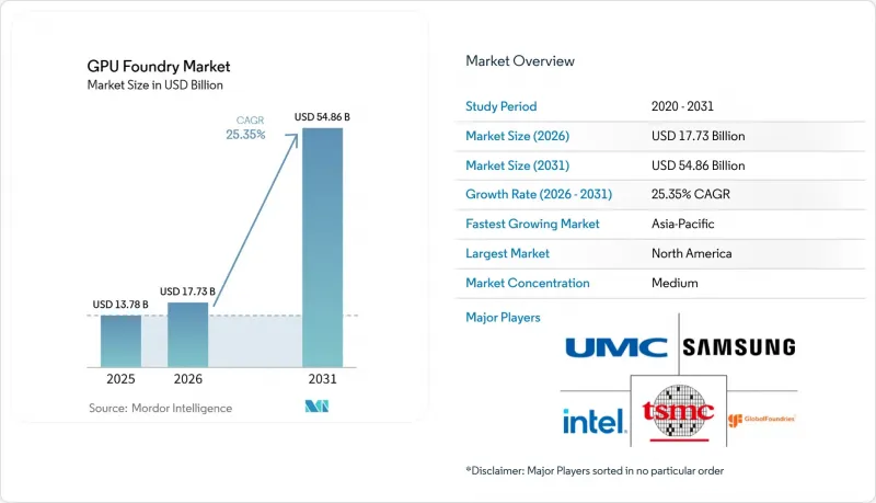
本報告按技術節點(3奈米及以下、4/5奈米、6/7奈米、8/10/12奈米、14/16奈米、20/22/28奈米及其他)、晶圓尺寸(300毫米、200毫米及其他)、代工經營模式(純晶圓代工市場預測以美元(USD)為單位。
全球GPU代工市場趨勢與洞察
超大規模人工智慧訓練與推理叢集擴展
隨著雲端平台人工智慧處理能力的提升和企業客戶推理應用場景的拓展,對超大規模領域的投資持續推動GPU代工市場的需求成長。現今,GPU代工市場既支援大規模訓練叢集,也支援持續推理部署,從而形成更穩定的產能補充週期,而非以往高階晶圓需求出現間歇性採購高峰。這一點至關重要,因為隨著效能要求的提高和服務延遲的日益關鍵化,人工智慧系統部署基地需要進行更新、擴展和區域複製。大型雲端公司內部加速器的擴張意味著GPU代工市場不再依賴單一晶片設計公司,越來越多的客製化晶片專案正在爭奪先進節點的產能。 NVIDIA宣布,位於鳳凰城的Blackwell晶圓生產已啟動,並計劃與合作夥伴在美國生產價值高達5000億美元的人工智慧基礎設施。這表明,人工智慧的需求正在推動尖端晶圓的啟動和下游系統製造產能的成長。
企業人工智慧工廠和主權運算採購
企業人工智慧工廠計畫和自主運算計畫正在為GPU代工市場創造更廣泛的需求基礎,使其不再完全依賴商業性最佳化。採購決策越來越受到彈性需求、對本土生產的偏好以及可靠供應鏈的限制,這提升了能夠跨多個地區提供認證生產能力的代工廠的價值。 2025年3月,台積電將其在美國的投資計畫擴大至1,650億美元,包括在亞利桑那州新建三座晶圓廠、兩座先進封裝廠和大規模研發中心。英偉達也表示,其在美國的人工智慧基礎設施製造網路現已擴展至半導體、基板、系統和機架等各個領域的合作夥伴,這印證了主權國家和企業買家正在尋求對其人工智慧硬體堆疊擁有更大的本地控制權。全球晶圓代工廠宣佈在美國投資160億美元,重點用於工廠擴建、封裝技術創新、矽光電和下一代氮化鎵技術,這表明它們正進一步積極參與美國國內市場。這證實了GPU晶圓代工廠市場採購方式的多元化,即使在最尖端科技仍然集中的領域也是如此。
出口限制和關稅波動
出口限制仍然是GPU代工市場面臨的最大外部限制因素,因為它同時影響最終目的地批准、客戶畫像和配額分配計畫。 2026年1月,美國工業與安全局(BIS)修改了對某些先進運算晶片出口到中國大陸和澳門的政策,將先前的「原則性拒絕」改為針對特定產品的「個案審查」。這項政策要求出口商證明,不會挪用面向美國終端用戶的類似或更先進晶片的全球代工廠產能,從而將代工廠配額與出口合規性直接掛鉤。因此,GPU代工市場面臨更繁瑣的文件和審查流程,以及哪些先進產品能夠順利進入生產線的不不確定性增加。雖然這種不確定性不會抑制需求,但卻讓整個GPU代工市場更難管理客戶優先順序、生產計畫和收入時間表。
細分市場分析
到2025年,4/5奈米製程將佔據GPU代工市場42.11%的佔有率,這一地位反映了目前AI加速器、高性能推理晶片和主要雲端客戶客製化晶片的主要生產階段。在GPU代工市場中,由於其電晶體密度、良率成熟度和生態系統發展相較於舊款和早期下一代製程節點具有更優的平衡性,該過程節點仍是商業性中心。此外,旗艦級AI產品在該製程節點下可以實現量產,而無需所有客戶在封裝、軟體和系統設計準備就緒之前就使用成本最高的製程節點。隨著遊戲產品、客戶端圖形、汽車控制器和工業推理設備等產品不斷延長更新週期,成熟的6/7奈米和8/10/12奈米等製程節點在GPU代工市場中繼續發揮重要作用。
預計到2031年,3nm以下製程製程將以26.21%的複合年成長率成長,成為成長最快的製程節點類別,因為GPU代工市場正向更節能的AI運算轉型。 NVIDIA和台積電宣布,首批Blackwell晶圓已在鳳凰城生產,台積電亞利桑那州工廠將生產2nm、3nm、4nm和A16製程的晶片。這證實了尖端AI產品與不斷擴大的5nm以下製造地之間存在著密切聯繫。英特爾進一步徵兆,Intel 18A將於2025年量產,Intel 18A-P將於2026年進入風險生產階段。這表明,儘管目前的GPU代工市場仍然集中,但未來最尖端科技的競爭正在日益激烈。實際上,GPU代工產業很可能採用分級節點結構,其中4/5nm仍是主要的商業基礎,3nm及以下節點則滿足高階AI的需求,而成熟節點則繼續用於處理對成本敏感且要求極高的產品。這意味著,儘管GPU代工市場尚未完全放棄舊節點,但其價值成長的更大佔有率正集中在先進節點層級,因為該層級的設計複雜性和定價能力都更強。
至2025年,300mm晶圓將佔GPU代工市場規模的96.33%,並將成為成長最快的晶圓尺寸細分市場,到2031年複合年成長率將達到26.62%。 GPU代工市場之所以能夠佔據主導地位,是因為300mm晶圓在更大晶片設計、提高單次生產良率以及在高成本先進製程節點上高效利用產能方面具有顯著的經濟優勢。在GPU代工產業,200mm晶圓仍用於生產專用控制器、電源組件和一些較老的圖形相關設備,因為轉向更大尺寸晶圓並不能帶來足夠的獲利。 150mm及以下尺寸的晶圓在GPU代工市場中仍佔較小佔有率,主要限於基板及相關組件的製造,而非主流GPU晶圓製造。
300mm晶圓在GPU代工市場的重要性不僅限於前端邏輯製造,還延伸至支撐最新AI設備的更廣泛的封裝生態系統。台積電宣佈在亞利桑那州的擴建計畫包括兩座先進封裝工廠,這標誌著其在晶圓製造和後端整合方面的300mm基礎得到加強。全球晶圓代工廠也致力於投資美國的封裝創新和矽光電,這表明美國的半導體策略正圍繞著更廣泛的製造鏈構建,而不僅僅是孤立的晶圓廠。因此,GPU代工市場很可能繼續高度依賴300mm基礎設施,而製程成熟度、封裝相容性和產能投資都在同步推進。
區域分析
到2025年,北美將佔據GPU代工市場68.44%的佔有率,這一主導地位主要歸功於該地區聚集了大量無晶圓廠AI晶片設計公司、超大規模資料中心業者和系統開發公司,這些公司推動了大部分尖端需求。因此,儘管晶圓製造歷來集中在東亞,但北美GPU代工市場仍以需求和設計為中心。 2025年3月,台積電將其在美國的投資計畫擴大至1,650億美元,包括在亞利桑那州新建三座晶圓廠、兩座先進封裝廠和大規模研發中心。英偉達也宣布,位於鳳凰城的Blackwell晶圓廠已開始投產,並計畫與合作夥伴在美國生產價值高達5,000億美元的AI基礎設施。這表明該地區的企業發展正在從晶片設計擴展到物理製造和系統構建。這使得北美成為GPU代工市場的商業性中心,儘管依賴跨國製造仍然是一個重大的策略風險。
預計到2031年,亞太地區GPU代工市場將以26.42%的複合年成長率成長,成為全球GPU代工市場規模成長最快的地區。台灣在尖端製造領域的核心地位是該地區GPU代工市場發展的基石,而來自日本、韓國和印度的投資也進一步擴大了其市場規模。 Cadence和三星晶圓代工計畫於2026年深化在2nm和3D-IC領域的合作,協助韓國在下一代人工智慧設計和製造領域保持領先地位。推動亞太地區GPU代工市場成長的關鍵因素包括其龐大的市場規模、穩健的供應鏈,以及該地區大部分先進節點製造產能的集中。
儘管歐洲在GPU代工市場中所佔佔有率仍然相對較小,但憑藉政策支援、可靠的製造系統和專業的半導體技術能力,其重要性正在不斷提升。全球晶圓代工廠已宣布將在2025年投資160億美元,用於擴大封裝和光電業務,這反映出歐洲為確保全部區域擁有強大的半導體產能而做出的更廣泛努力。南美和中東及非洲在GPU代工市場中所佔佔有率仍然有限,但中東作為國家主導的人工智慧基礎設施需求中心,其重要性日益凸顯。這些地區在GPU代工市場中將扮演的長期角色,可能更取決於運算能力的普及、互聯互通的改善以及可靠的採購夥伴關係,而非短期內在其各自國家建設大規模、最先進的晶圓廠產能。
其他好處:
- Excel格式的市場預測(ME)表
- 3個月的分析師支持
目錄
第1章:引言
- 研究假設和市場定義
- 調查範圍
第2章:調查方法
第3章執行摘要
第4章 市場狀況
- 市場概覽
- 市場促進因素
- 規模化超大規模人工智慧訓練與推理集群
- 企業人工智慧工廠和主權運算採購
- 基於晶片組的GPU藍圖提高了良率和產品擴展性。
- 利用低於5奈米的先進製程的人工智慧加速器競爭
- 產業對高可靠性國產晶圓廠的需求
- 透過長期人工智慧供應合約固定代工廠產能
- 市場限制因素
- 出口限制和關稅波動
- GPU 和記憶體的平均售價 (ASP) 持續居高不下,減緩了它們在主流市場的普及。
- HBM 和先進封裝的分配嚴重偏向 AI 機架。
- 高密度GPU園區電網連接延遲
- 產業價值鏈分析
- 產業供應鏈分析
- 宏觀經濟因素對市場的影響
- 監理情勢
- 技術展望
- 波特五力分析
第5章 市場規模與成長預測
- 依技術節點
- 3牛頓米或更小
- 4/5 Nm
- 6/7 Nm
- 8/10/12 Nm
- 14/16 Nm
- 20/22/28 Nm
- 40/45/55 Nm
- 65牛頓米或以上
- 按晶圓尺寸
- 300 mm
- 200 mm
- 150毫米或更小
- 鑄造經營模式
- 專業鑄造廠
- IDM商戶代工服務
- 透過使用
- 資料中心、人工智慧、高效能運算
- 客戶端計算和遊戲
- 商用的可視化和工作站
- 車
- 工業、邊緣人工智慧、物聯網、機器人
- 消費性電子產品和行動圖形
- 其他用途
- 按地區
- 北美洲
- 美國
- 加拿大
- 墨西哥
- 歐洲
- 德國
- 英國
- 法國
- 義大利
- 其他歐洲國家
- 俄羅斯
- 亞太地區
- 中國
- 日本
- 韓國
- 印度
- 東南亞
- 其他亞太國家
- 南美洲
- 巴西
- 阿根廷
- 其他南美國家
- 中東
- 沙烏地阿拉伯
- 阿拉伯聯合大公國
- 土耳其
- 其他中東國家
- 非洲
- 南非
- 其他非洲國家
- 北美洲
第6章 競爭情勢
- 市場集中度
- 策略趨勢
- Market Positioning Analysis
- 公司簡介
- Taiwan Semiconductor Manufacturing Company Limited
- Samsung Electronics Co., Ltd.
- Intel Corporation
- GlobalFoundries Inc.
- United Microelectronics Corporation
- Semiconductor Manufacturing International Corporation
- Tower Semiconductor Ltd.
- Hua Hong Semiconductor Limited
- Powerchip Semiconductor Manufacturing Corporation
- Vanguard International Semiconductor Corporation
- X-FAB Silicon Foundries SE
- SkyWater Technology, Inc.
- STMicroelectronics NV
- Renesas Electronics Corporation
- Dongbu HiTek Co., Ltd.
- PSMC Group
- ASE Technology Holding Co., Ltd.
- Amkor Technology, Inc.
- JCET Group Co., Ltd.
- SMIC Shanghai Manufacturing Co.
第7章 市場機會與未來展望
According to Mordor Intelligence, the GPU foundry market size is expected to increase from USD 13.78 billion in 2025 to USD 17.73 billion in 2026 and reach USD 54.86 billion by 2031, growing at a CAGR of 25.35% over 2026-2031.
This report is Segmented by Technology Node (3 Nm and Below, 4/5 Nm, 6/7 Nm, 8/10/12 Nm, 14/16 Nm, 20/22/28 Nm, and More), Wafer Size (300 Mm, 200 Mm, and More), Foundry Business Model (Pure-Play Foundry, and IDM Merchant Foundry Services), Application (Data Center AI and HPC, Client Computing and Gaming, Automotive, Industrial, and More), and Geography. The Market Forecasts are Provided in Terms in Value (USD).
Global GPU Foundry Market Trends and Insights
Hyperscale AI Training and Inference Cluster Expansion
Hyperscale spending remains the main demand engine for the GPU foundry market because cloud platforms are building AI capacity at the same time that enterprise customers are broadening inference use cases. The GPU foundry market now supports both large training clusters and recurring inference deployments, and that creates a steadier replenishment cycle for high-end wafer demand than one-off procurement waves. This matters because the installed base of AI systems has to be refreshed, expanded, and regionally duplicated as performance requirements rise and service latency becomes more important. The growth of in-house accelerators at major cloud firms also means the GPU foundry market is no longer tied to a single chip designer, since more custom silicon programs now compete for advanced-node capacity. NVIDIA stated that Blackwell wafer production is underway in Phoenix and that it plans to produce up to USD 500 billion of AI infrastructure in the US with partners, which shows how AI demand is now pulling on both leading-edge wafer starts and downstream system manufacturing capacity.
Enterprise AI Factory and Sovereign Compute Procurement
Enterprise AI factory programs and sovereign compute plans are giving the GPU foundry market a broader demand base that is less dependent on pure commercial optimization. Procurement is increasingly shaped by resilience, domestic production preferences, and the need for trusted supply, which raises the value of foundries that can point to certified capacity across more than one geography. TSMC expanded its planned US investment to USD 165 billion in March 2025, and that package includes three new fabs, two advanced packaging facilities, and a major R&D center in Arizona.NVIDIA also said its US manufacturing network for AI infrastructure now spans partners across semiconductors, boards, systems, and racks, which supports the view that sovereign and enterprise buyers want more local control over the AI hardware stack. GlobalFoundries added another domestic signal with a USD 16 billion US investment focused on facility expansion, packaging innovation, silicon photonics, and next-generation GaN, and that supports a wider sourcing field inside the GPU foundry market even where leading-edge share remains concentrated.
Export Controls and Tariff Volatility
Export controls remain the most disruptive external restraint for the GPU foundry market because they affect end-destination approval, customer mix, and allocation planning at the same time. The US Bureau of Industry and Security changed its policy on certain advanced computing chip exports to China and Macau in January 2026, shifting from a presumption of denial to a case-by-case review for specified products. That policy also requires exporters to certify that global foundry capacity for similar or more advanced chips for US end users will not be diverted, which ties foundry allocation directly to export compliance. The result is that the GPU foundry market faces more documentation, more screening, and less certainty around which advanced products can move through the pipeline without delay. This uncertainty does not stop demand, but it does make customer prioritization, production planning, and revenue timing harder to manage across the GPU foundry market.
Other drivers and restraints analyzed in the detailed report include:
- AI Accelerator Race for Sub-5 Nm Advanced Nodes
- Chiplet-Based GPU Roadmaps Improving Yield and Product Scaling
- HBM and Advanced Packaging Allocation Bias Toward AI Racks
For complete list of drivers and restraints, kindly check the Table Of Contents.
Segment Analysis
The 4/5 nm segment held 42.11% of the GPU foundry market share in 2025, and that position reflected the main production generation for current AI accelerators, high-performance inference chips, and custom silicon from large cloud customers. In the GPU foundry market, this node band remains the commercial center because it balances transistor density, yield maturity, and ecosystem readiness better than older nodes and better than very early next-generation ramps. It also sits at the point where flagship AI products can be produced at scale without forcing every customer onto the highest-cost node before packaging, software, and system design are ready. Mature clusters such as 6/7 nm and 8/10/12 nm still matter in the GPU foundry market because gaming products, client graphics, automotive controllers, and industrial inference devices continue to ship on longer refresh cycles.
The 3 nm and below segment is projected to expand at a 26.21% CAGR through 2031, and that makes it the fastest node category as the GPU foundry market moves toward more power-efficient AI compute. NVIDIA and TSMC said the first Blackwell wafer was produced in Phoenix and that TSMC Arizona will produce 2 nm, 3 nm, 4 nm, and A16 technologies, which reinforces the practical link between advanced AI products and a widening sub-5 nm manufacturing footprint. Intel added another signal when it said Intel 18A entered production in 2025 and Intel 18A-P entered risk production in 2026, which shows that future leading-edge competition is becoming more credible even if the current GPU foundry market remains concentrated. In practice, the GPU foundry industry is likely to run with a layered node structure where 4/5 nm remains a large commercial base, 3 nm and below captures the premium AI migration, and mature nodes keep serving cost-sensitive and qualification-heavy products. This means the GPU foundry market is not moving away from older nodes entirely, but it is placing more of its value growth in the advanced-node tier where design complexity and pricing power are strongest.
The 300 mm segment commanded 96.33% of GPU foundry market size in 2025, and it also stands as the fastest-growing wafer size segment with a 26.62% CAGR through 2031. That dominance is expected because the GPU foundry market relies on 300 mm economics for large die designs, better output per run, and more efficient use of expensive advanced-node capacity. In the GPU foundry industry, 200 mm production still has a role in specialty controllers, power components, and older graphics-related devices where migration to larger wafers would not improve returns enough to justify the shift. The 150 mm and below tier remains marginal in the GPU foundry market and is mainly tied to supporting substrates or adjacent components rather than mainstream GPU wafer fabrication.
The importance of 300 mm wafers in the GPU foundry market extends beyond front-end logic production and into the broader packaging ecosystem that supports modern AI devices. TSMC said its Arizona expansion includes two advanced packaging facilities, which means the 300 mm footprint is being reinforced across both wafer fabrication and back-end integration. GlobalFoundries also committed funding to packaging innovation and silicon photonics in the US, which shows that domestic semiconductor strategy is being built around broader manufacturing chains and not just standalone fab shells. As a result, the GPU foundry market is likely to remain overwhelmingly tied to 300 mm infrastructure because that is where process maturity, packaging compatibility, and capacity investment are all moving together.
Complete Report Scope:
- By Technology Node
- 3 Nm and Below
- 4/5 Nm
- 6/7 Nm
- 8/10/12 Nm
- 14/16 Nm
- 20/22/28 Nm
- 40/45/55 Nm
- 65 Nm and Above
- By Wafer Size
- 300 Mm
- 200 Mm
- 150 Mm and Below
- By Foundry Business Model
- Pure-Play Foundry
- IDM Merchant Foundry Services
- By Application
- Data Center AI and HPC
- Client Computing and Gaming
- Professional Visualization and Workstations
- Automotive
- Industrial, Edge AI, IoT, and Robotics
- Consumer Electronics and Mobile Graphics
- Other Applications
- By Geography
- North America
- United States
- Canada
- Mexico
- Europe
- Germany
- United Kingdom
- France
- Italy
- Rest of Europe
- Russia
- Asia-Pacific
- China
- Japan
- South Korea
- India
- Southeast Asia
- Rest of Asia-Pacific
- South America
- Brazil
- Argentina
- Rest of South America
- Middle East
- Saudi Arabia
- United Arab Emirates
- Turkey
- Rest of Middle East
- Africa
- South Africa
- Rest of Africa
- North America
Geography Analysis
North America held 68.44% of the GPU foundry market share in 2025, and that lead came from the region's concentration of fabless AI chip designers, hyperscalers, and system developers that drive most leading-edge demand. The GPU foundry market in North America is therefore demand-heavy and design-heavy, even though a large share of wafer fabrication has historically remained concentrated in East Asia. TSMC expanded its planned US investment to USD 165 billion in March 2025, and the package covers three new fabs, two advanced packaging facilities, and a major RandD center in Arizona. NVIDIA also said Blackwell wafer production is underway in Phoenix and that it plans to produce up to USD 500 billion of AI infrastructure in the US with partners, which shows that the regional footprint is extending from silicon design into physical manufacturing and system buildout. This makes North America the commercial center of the GPU foundry market even as cross-border manufacturing dependence remains an important strategic risk.
Asia-Pacific is projected to expand at a 26.42% CAGR, making it the fastest-growing contributor to GPU foundry market size through 2031. The GPU foundry market in this region remains anchored by Taiwan's central role in leading-edge fabrication, but it is also being widened by investment paths linked to Japan, South Korea, and India. Cadence and Samsung Foundry deepened their 2 nm and 3D-IC collaboration in 2026, which supports South Korea's effort to stay relevant in next-generation AI design and manufacturing flows. The region's growth profile in the GPU foundry market comes from scale, supply chain depth, and the fact that most practical advanced-node manufacturing capacity is still clustered there.
Europe remains a smaller part of the GPU foundry market, but it is gaining relevance through policy support, trusted manufacturing, and specialty semiconductor capabilities. GlobalFoundries announced a USD 16 billion US investment in 2025 that included packaging and photonics expansion, and that kind of industrial policy response mirrors the broader push for resilient semiconductor capacity across allied regions. South America, the Middle East, and Africa still represent a limited share of the GPU foundry market, although the Middle East is becoming more important as a demand center for sovereign AI infrastructure. The long-term role of these regions in the GPU foundry market is likely to depend more on compute deployment, connectivity upgrades, and trusted sourcing partnerships than on near-term creation of large domestic leading-edge fab capacity.
- Taiwan Semiconductor Manufacturing Company Limited
- Samsung Electronics Co., Ltd.
- Intel Corporation
- GlobalFoundries Inc.
- United Microelectronics Corporation
- Semiconductor Manufacturing International Corporation
- Tower Semiconductor Ltd.
- Hua Hong Semiconductor Limited
- Powerchip Semiconductor Manufacturing Corporation
- Vanguard International Semiconductor Corporation
- X-FAB Silicon Foundries SE
- SkyWater Technology, Inc.
- STMicroelectronics N.V.
- Renesas Electronics Corporation
- Dongbu HiTek Co., Ltd.
- PSMC Group
- ASE Technology Holding Co., Ltd.
- Amkor Technology, Inc.
- JCET Group Co., Ltd.
- SMIC Shanghai Manufacturing Co.
Additional Benefits:
- The market estimate (ME) sheet in Excel format
- 3 months of analyst support
TABLE OF CONTENTS
1 INTRODUCTION
- 1.1 Study Assumptions and Market Definition
- 1.2 Scope of the Study
2 RESEARCH METHODOLOGY
3 EXECUTIVE SUMMARY
4 MARKET LANDSCAPE
- 4.1 Market Overview
- 4.2 Market Drivers
- 4.2.1 Hyperscale AI Training and Inference Cluster Expansion
- 4.2.2 Enterprise AI Factory and Sovereign Compute Procurement
- 4.2.3 Chiplet-Based GPU Roadmaps Improving Yield and Product Scaling
- 4.2.4 AI Accelerator Race for Sub-5 Nm Advanced Nodes
- 4.2.5 Industry Demand for Trusted Domestic Fabs
- 4.2.6 Foundry Capacity Lock-In Through Long-Term AI Supply Agreements
- 4.3 Market Restraints
- 4.3.1 Export Controls and Tariff Volatility
- 4.3.2 Elevated GPU and Memory ASPs Slowing Mainstream Adoption
- 4.3.3 HBM and Advanced Packaging Allocation Bias Toward AI Racks
- 4.3.4 Grid Interconnection Delays for High-Density GPU Campuses
- 4.4 Industry Value Chain Analysis
- 4.5 Industry Supply Chain Analysis
- 4.6 Impact of Macroeconomic Factors on the Market
- 4.7 Regulatory Landscape
- 4.8 Technological Outlook
- 4.9 Porter's Five Forces Analysis
- 4.9.1 Bargaining Power of Suppliers
- 4.9.2 Bargaining Power of Buyers
- 4.9.3 Threat of New Entrants
- 4.9.4 Threat of Substitutes
- 4.9.5 Intensity of Competitive Rivalry
5 MARKET SIZE AND GROWTH FORECASTS (VALUE)
- 5.1 By Technology Node
- 5.1.1 3 Nm and Below
- 5.1.2 4/5 Nm
- 5.1.3 6/7 Nm
- 5.1.4 8/10/12 Nm
- 5.1.5 14/16 Nm
- 5.1.6 20/22/28 Nm
- 5.1.7 40/45/55 Nm
- 5.1.8 65 Nm and Above
- 5.2 By Wafer Size
- 5.2.1 300 Mm
- 5.2.2 200 Mm
- 5.2.3 150 Mm and Below
- 5.3 By Foundry Business Model
- 5.3.1 Pure-Play Foundry
- 5.3.2 IDM Merchant Foundry Services
- 5.4 By Application
- 5.4.1 Data Center AI and HPC
- 5.4.2 Client Computing and Gaming
- 5.4.3 Professional Visualization and Workstations
- 5.4.4 Automotive
- 5.4.5 Industrial, Edge AI, IoT, and Robotics
- 5.4.6 Consumer Electronics and Mobile Graphics
- 5.4.7 Other Applications
- 5.5 By Geography
- 5.5.1 North America
- 5.5.1.1 United States
- 5.5.1.2 Canada
- 5.5.1.3 Mexico
- 5.5.2 Europe
- 5.5.2.1 Germany
- 5.5.2.2 United Kingdom
- 5.5.2.3 France
- 5.5.2.4 Italy
- 5.5.2.5 Rest of Europe
- 5.5.2.6 Russia
- 5.5.3 Asia-Pacific
- 5.5.3.1 China
- 5.5.3.2 Japan
- 5.5.3.3 South Korea
- 5.5.3.4 India
- 5.5.3.5 Southeast Asia
- 5.5.3.6 Rest of Asia-Pacific
- 5.5.4 South America
- 5.5.4.1 Brazil
- 5.5.4.2 Argentina
- 5.5.4.3 Rest of South America
- 5.5.5 Middle East
- 5.5.5.1 Saudi Arabia
- 5.5.5.2 United Arab Emirates
- 5.5.5.3 Turkey
- 5.5.5.4 Rest of Middle East
- 5.5.6 Africa
- 5.5.6.1 South Africa
- 5.5.6.2 Rest of Africa
- 5.5.1 North America
6 COMPETITIVE LANDSCAPE
- 6.1 Market Concentration
- 6.2 Strategic Moves
- 6.3 Market Positioning Analysis
- 6.4 Company Profiles (includes Global Level Overview, Market Level Overview, Core Segments, Financials as available, Strategic Information, Market Rank/Share, Products and Services, Recent Developments)
- 6.4.1 Taiwan Semiconductor Manufacturing Company Limited
- 6.4.2 Samsung Electronics Co., Ltd.
- 6.4.3 Intel Corporation
- 6.4.4 GlobalFoundries Inc.
- 6.4.5 United Microelectronics Corporation
- 6.4.6 Semiconductor Manufacturing International Corporation
- 6.4.7 Tower Semiconductor Ltd.
- 6.4.8 Hua Hong Semiconductor Limited
- 6.4.9 Powerchip Semiconductor Manufacturing Corporation
- 6.4.10 Vanguard International Semiconductor Corporation
- 6.4.11 X-FAB Silicon Foundries SE
- 6.4.12 SkyWater Technology, Inc.
- 6.4.13 STMicroelectronics N.V.
- 6.4.14 Renesas Electronics Corporation
- 6.4.15 Dongbu HiTek Co., Ltd.
- 6.4.16 PSMC Group
- 6.4.17 ASE Technology Holding Co., Ltd.
- 6.4.18 Amkor Technology, Inc.
- 6.4.19 JCET Group Co., Ltd.
- 6.4.20 SMIC Shanghai Manufacturing Co.
7 MARKET OPPORTUNITIES AND FUTURE OUTLOOK
- 7.1 White-Space and Unmet-Need Assessment

 動態圖像設計服務市場:全球市場預測,2026-2032年
 2026年全球人工智慧(AI)資料中心圖形處理器(GPU)市場報告2026年人工智慧圖形處理器(GPU)全球市場報告2026年深度學習圖形處理器(GPU)全球市場報告2026年全球混合圖形處理器(GPU)市場報告
 全球圖形處理器(GPU)市場規模、佔有率、趨勢和成長分析報告(2026-2034年)
 圖形處理器:市場佔有率分析、產業趨勢與統計、成長預測(2026-2031)GPU(影像處理)市場:按產品類型、記憶體類型、散熱方式、部署方式、應用和最終用戶分類 - 全球市場預測(2026-2032 年)GPU網路:市佔率分析、產業趨勢與統計、成長預測(2026-2031年)GPU軟體:市佔率分析、產業趨勢與統計、成長預測(2026-2031年)