


 |
市場調查報告書
商品編碼
2098536
DRAM記憶體介面IP:市場佔有率分析、產業趨勢與統計、成長預測(2026-2031年)DRAM Memory Interface IP - Market Share Analysis, Industry Trends & Statistics, Growth Forecasts (2026 - 2031) |
||||||

※ 本網頁內容可能與最新版本有所差異。詳細情況請與我們聯繫。
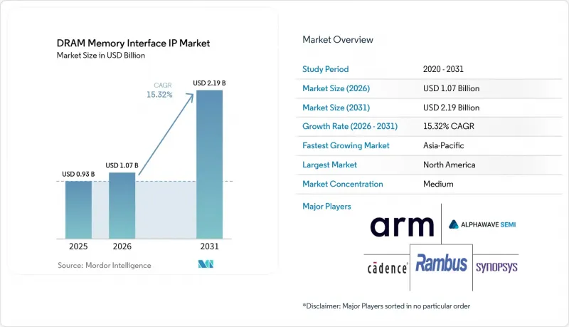
根據 Mordor Intelligence 預測,DRAM 記憶體介面 IP 市場規模預計將在 2025 年達到 9.3 億美元,2026 年達到 10.7 億美元,2031 年達到 21.9 億美元,2026 年至 2031 年的複合年成長率為 15.32%。
本報告按記憶體介面架構(DDR 和 DIMM 記憶體介面 IP、LPDDR 記憶體介面 IP、GDDR 記憶體介面 IP、HBM 記憶體介面 IP)、應用領域(資料中心/雲端/高效能運算/人工智慧、行動和消費性電子設備、圖形/遊戲等)、客戶類型(無晶圓廠半導體公司等)以及區域進行細分。市場預測以美元計價。
全球DRAM記憶體介面IP市場趨勢及洞察
人工智慧、高效能運算和資料中心對記憶體頻寬的需求日益成長。
人工智慧訓練與推理工作負載使得記憶體頻寬成為高階加速器設計的核心阻礙因素,進而提升了DRAM記憶體介面IP市場的戰略地位。企業內部研發進度落後於競爭對手的人工智慧項目,導致買家越來越需要完整且經過矽驗證的控制器和PHY協議堆疊。在HBM專案中,這項需求尤其突出,子系統檢驗、封裝就緒性和互通性正成為採購決策的一部分,而非事後補救。這一趨勢導致動態隨機存取記憶體(DRAM)記憶體介面IP市場中認證供應商的選擇範圍縮小,因為能夠提供成熟平台以支援大規模人工智慧和高效能運算部署的供應商寥寥無幾。 2026年2月,Synopsys成功檢驗了一款採用3nm製程的9.2Gbps HBM4 IP測試晶片;同年3月,Rhambus推出了支援單腳高達16Gbps的HBM4E控制器IP。這些都表明,人工智慧的記憶體需求正在深刻影響當前的產品藍圖。
遷移到 LPDDR5X、GDDR7 和 HBM 相容介面
向LPDDR6、GDDR7和下一代HBM的過渡正在移動、圖形、人工智慧和伺服器等領域的DRAM記憶體介面IP市場引發廣泛的更新換代。 JEDEC於2025年發布了LPDDR6規範,其單腳資料速率高達14.4Gbps,並採用更寬的頻寬通道結構。這意味著供應商需要進行更全面的升級,而不僅僅是簡單的PHY小幅修改才能保持領先。 2025年7月,Cadence發布了其LPDDR6/5X 14.4Gbps記憶體IP系統解決方案,將新標準的採用與商用IP的可用性直接連結起來。這種快速的更新速度迫使DRAM記憶體介面IP市場供應商同時推進多條開發路線,不僅增加了研發壓力,也讓擁有更強大平台資源的供應商更具優勢。此外,客戶的計劃也在發生變化,許多買家現在更傾向於儘早確定下一代IP,以避免在標準過渡期陷入困境。
高階記憶體介面的高非重複工程成本和檢驗成本
高昂的開發和檢驗成本仍然是DRAM記憶體介面IP市場,特別是先進製程節點和HBM專案中,面臨的最明顯障礙。技術負擔不僅限於控制器和PHY設計,還包括封裝互動、確保互通性以及在多種工作條件下進行詳細的特性分析。 Synopsys的HBM4檢驗里程碑以及GUC在台積電3nm製程(CoWoS)上進行的12Gbps HBM4演示,都顯示了商業部署實現之前所需的技術深度。這種成本結構不僅縮小了能夠快速採用尖端IP的客戶群,也限制了供應商在後續標準開發方面的投資選擇。事實上,儘管DRAM記憶體介面IP市場持續成長,但對於大型供應商和資金雄厚的買家而言,獲得其最高價值層級的產品仍然比小規模新參與企業更容易。
細分市場分析
2025年,DDR和DIMM記憶體介面IP佔據DRAM記憶體介面IP市場佔有率的39.21%,主要得益於DDR5和MRDIMM介面在雲端、企業和AI伺服器系統中的廣泛應用。隨著伺服器平台在不放棄現有DDR生態系統的前提下不斷提升記憶體頻寬, DRAM記憶體介面IP市場的這一細分領域依然保持強勁成長勢頭。 2025年4月,Cadence發布了基於台積電N3製程的DDR5 12.8Gbps MRDIMM Gen2記憶體IP系統解決方案,面向AI雲端和企業資料中心,進一步推動了市場需求。此外,隨著新標準與汽車運算、邊緣AI和低功耗伺服器記憶體應用相結合,LPDDR的重要性也持續超越行動電話。
JEDEC 2025 年發布的 LPDDR6 文件概述了每引腳 14.4 Gbps 的傳輸速率以及通道架構的擴展,這為面向移動和推理工作負載的供應商開啟了新的開發週期。 Cadence 隨後發布了其 LPDDR6/5X 系統解決方案,表明標準制定正迅速轉化為產品發布。 HBM 記憶體介面 IP 預計到 2031 年將以 16.12% 的複合年成長率成長,並且隨著 AI 加速器和 GPU 專案向 HBM4 和 HBM4E 週期過渡,有望成為 DRAM 記憶體介面 IP 市場中成長最快的架構。 Lambuth 於 2026 年 3 月發布了其 HBM4E 控制器 IP,GUC 於 2026 年 4 月展示了 12 Gbps 的 HBM4 平台。這表明 HBM 正在成為一個更廣泛的子系統,涵蓋控制器邏輯、PHY 設計、封裝支援和模擬相關文檔,從而帶來新的機會。
區域分析
預計到2025年,北美將佔據DRAM記憶體介面IP市場佔有率的39.51%,成為最大的區域貢獻者。該地區受益於超大規模資料中心業者、AI晶片開發商和主要平台IP供應商的高度集中,從而在市場前沿領域保持了異常活躍的設計活動。 Synopsys、Cadence和Lambuth憑藉其在HBM、DDR和LPDDR平台領域的領先地位,繼續引領著源自北美的大部分高價值專案。此外,北美專案通常與客製化AI晶片和大規模雲端基礎設施的藍圖緊密相關,從而促成高價值的長期合約。因此,儘管買家數量有限,但該地區的DRAM記憶體介面IP市場仍保持強勁勢頭。
歐洲憑藉其對汽車半導體的需求以及以安全為中心的認證要求,保持著獨特的地位。該地區的汽車零件供應商需要能夠滿足不斷成長的汽車頻寬和長產品生命週期需求的內存介面,這推動了對經過認證的LPDDR和未來GDDR解決方案的持續需求。 JEDEC的汽車產業指南明確指出,高性能記憶體正成為先進汽車人工智慧系統不可或缺的一部分,同時合規性要求依然十分嚴格。歐洲在供應方面也發揮著重要作用,其設計和檢驗能力與先進封裝工作流程密切相關。西門子EDA的HBM封裝指南表明,記憶體介面規劃與系統和封裝的協同設計日益緊密相連,這進一步鞏固了歐洲在技術實現方面的地位,即使其直接授權規模小於北美。
預計到2031年,亞太地區將以16.28%的複合年成長率成長,成為DRAM記憶體介面IP市場成長最快的地區。台灣和韓國仍然是該市場的核心,先進的封裝和HBM生產集中在這些市場。 GUC採用台積電3nm製程及CoWoS技術展示HBM4,體現了台灣在推動最新封裝相關記憶體介面走向量產方面所扮演的角色。韓國在IP供應方面的影響力也不斷增強,OPENEDGES於2026年4月簽署了其首個LPDDR6和LPDDR5X內存子系統IP的商業授權合約。中國正在推動記憶體介面IP的本土化,Innosilicon於2026年1月交付了中國首個LPDDR6和LPDDR5X組合PHY及控制器,這標誌著朝著這個方向邁出了重要一步。儘管日本仍然是汽車和工業需求的重要市場,但世界其他地區透過設計服務和與更廣泛的亞太供應鏈相關的綜合支持,繼續看到市場逐步擴張。
其他好處:
- Excel格式的市場預測(ME)表
- 3個月的分析師支持
目錄
第1章:引言
- 研究假設和市場定義
- 調查範圍
第2章:調查方法
第3章執行摘要
第4章 市場狀況
- 市場概覽
- 市場促進因素
- 人工智慧、高效能運算和資料中心對記憶體頻寬的需求日益成長。
- 遷移到 LPDDR5X、GDDR7 和 HBM 相容介面
- 晶片級封裝和先進封裝技術的應用日益普及。
- 汽車高級駕駛輔助系統和車載計算中的記憶體複雜度
- 更短的設計週期有利於重複使用預先檢驗的智慧財產權。
- 記憶體安全性、可靠性和訊號完整性的要求
- 市場限制因素
- 高階記憶體介面的高非重複工程成本和檢驗成本
- 基本客群狹窄,認證週期長
- DRAM 標準的快速發展可能會導致智慧財產權過時。
- 跨流程節點和包的整合複雜性
- 宏觀經濟因素對市場的影響
- 產業價值鏈分析
- 供應鏈分析
- 監理情勢
- 技術展望
- 波特五力分析
第5章 市場規模與成長預測
- 透過記憶體介面架構
- DDR和DIMM記憶體介面IP
- LPDDR記憶體介面IP
- GDDR記憶體介面IP
- HBM 記憶體介面 IP
- 透過使用
- 資料中心/雲端運算/高效能運算/人工智慧
- 行動和消費設備
- 圖形/遊戲
- 汽車/ADAS
- 工業/物聯網/網路
- 依客戶類型
- 無晶圓廠半導體公司
- IDMs
- 系統OEM
- 超大規模資料中心業者
- 按地區
- 北美洲
- 歐洲
- 亞太地區
- 中國
- 日本
- 韓國
- 台灣
- 其他亞太國家
- 世界其他地區
第6章 競爭情勢
- 市場集中度
- 策略趨勢
- 市佔率分析
- 公司簡介
- Synopsys, Inc.
- Cadence Design Systems, Inc.
- Rambus Inc.
- Alphawave IP Group plc
- Arm Limited
- Siemens EDA
- Ansys, Inc.
- Silicon Creations, LLC
- VeriSilicon Microelectronics(Shanghai)Co., Ltd.
- Imagination Technologies Limited
- Broadcom Inc.
- Qualcomm Technologies, Inc.
- Marvell Technology, Inc.
- Intel Corporation
- Advanced Micro Devices, Inc.
- Samsung Electronics Co., Ltd.
- Micron Technology, Inc.
- SK hynix Inc.
- NXP Semiconductors NV
- Texas Instruments Incorporated
第7章 市場機會與未來展望
According to Mordor Intelligence, the DRAM memory interface IP market size is projected to be USD 0.93 billion in 2025, USD 1.07 billion in 2026, and reach USD 2.19 billion by 2031, growing at a CAGR of 15.32% from 2026 to 2031.
This report is Segmented by Memory Interface Architecture (DDR and DIMM Memory Interface IP, LPDDR Memory Interface IP, GDDR Memory Interface IP, and HBM Memory Interface IP), Application (Data Center/Cloud/HPC/AI, Mobile and Consumer Devices, Graphics/Gaming, and More), Customer Type (Fabless Semiconductor Companies, and More), and Geography. The Market Forecasts are Provided in Terms of Value (USD).
Global DRAM Memory Interface IP Market Trends and Insights
Rising AI, HPC, and Data Center Memory Bandwidth Requirements
AI training and inference workloads have made memory bandwidth a central design constraint for advanced accelerators, elevating the strategic role of the DRAM memory interface IP market. Buyers increasingly need complete controller and PHY stacks that are already silicon-proven, because in-house development no longer aligns with the timing of competitive AI programs. That requirement is especially clear in HBM programs, where subsystem validation, packaging readiness, and interoperability have become part of the buying decision rather than follow-on work. This trend is tightening the qualified vendor pool in the dynamic random-access memory (DRAM) memory interface IP market, because only a few suppliers can support large AI and HPC deployments with proven platforms. Synopsys validated an HBM4 IP test chip at 9.2Gbps on a 3nm process in February 2026, and Rambus launched HBM4E controller IP rated up to 16Gbps per pin in March 2026, showing how strongly AI memory requirements are shaping current product roadmaps.
Migration To LPDDR5X, GDDR7, and HBM-Linked Interfaces
The move to LPDDR6, GDDR7, and newer HBM generations is creating a broad replacement cycle across mobile, graphics, AI, and server programs in the DRAM memory interface IP market. JEDEC presented LPDDR6 features in 2025 with data rates up to 14.4Gbps per pin and wider channel structures, which means suppliers need more than a minor PHY revision to stay current. Cadence launched an LPDDR6/5X 14.4Gbps memory IP system solution in July 2025, which linked new standard adoption directly to commercial IP availability. This pace is forcing vendors in the DRAM memory interface IP market to maintain multiple development tracks simultaneously, increasing R&D pressure and favoring suppliers with deeper platform resources. It also changes customer timing, because many buyers now prefer to lock in next-generation IP earlier to avoid getting trapped between one standard transition and the next.
High NRE and Validation Cost for Advanced Memory Interfaces
High development and validation costs remain the clearest brake on the DRAM memory interface IP market, especially at advanced nodes and in HBM programs. The technical burden now extends beyond controller and PHY design into package interaction, interoperability work, and deep characterization across multiple operating conditions. Synopsys's HBM4 validation milestone and GUC's 12Gbps HBM4 demonstration on TSMC's 3nm with CoWoS show the engineering depth required before commercial deployment becomes credible. That cost structure narrows the pool of customers that can quickly adopt the most advanced IP, and it also narrows the pool of vendors that can fund development across successive standards. In practical terms, the DRAM memory interface IP market continues to grow, but its highest-value tiers remain easier for large vendors and well-capitalized buyers to access than for smaller entrants.
Other drivers and restraints analyzed in the detailed report include:
- Increasing Chiplet-Based and Advanced Package Adoption
- Automotive ADAS and In-Vehicle Compute Memory Complexity
- Limited Customer Base and Long Qualification Cycles
For complete list of drivers and restraints, kindly check the Table Of Contents.
Segment Analysis
DDR and DIMM memory interface IP held 39.21% of the DRAM memory interface IP market share in 2025, supported by the broad installed base of DDR5 and MRDIMM interfaces in cloud, enterprise, and AI server systems. This part of the DRAM memory interface IP market remained active because server platforms continued to upgrade memory bandwidth without abandoning the familiar DDR ecosystem. Cadence reinforced that demand in April 2025 when it introduced a DDR5 12.8Gbps MRDIMM Gen2 memory IP system solution on TSMC N3 for AI cloud and enterprise data center deployments. LPDDR also continued to expand its relevance beyond handsets, as newer standards are now tied to automotive compute, edge AI, and low-power server memory applications.
JEDEC's 2025 LPDDR6 materials showed a move to 14.4 Gbps per pin and broader channel structures, opening a new development cycle for suppliers serving mobile and inference workloads. Cadence followed that transition with its LPDDR6/5X system solution, showing how quickly standards activity is translating into product launches. HBM memory interface IP is projected to grow at a 16.12% CAGR through 2031, making it the fastest-growing architecture in the DRAM memory interface IP market as AI accelerators and GPU programs move into HBM4 and HBM4E cycles. Rambus introduced HBM4E controller IP in March 2026, and GUC demonstrated a 12Gbps HBM4 platform in April 2026, which shows that HBM is becoming a broader subsystem opportunity that includes controller logic, PHY design, package support, and simulation collateral.
Complete Report Scope:
- By Memory Interface Architecture
- DDR and DIMM Memory Interface IP
- LPDDR Memory Interface IP
- GDDR Memory Interface IP
- HBM Memory Interface IP
- By Application
- Data Center/Cloud/HPC/AI
- Mobile and Consumer Devices
- Graphics/Gaming
- Automotive/ADAS
- Industrial/IoT/Networking
- By Customer Type
- Fabless Semiconductor Companies
- IDMs
- System OEMs
- Hyperscalers
- By Geography
- North America
- Europe
- Asia-Pacific
- China
- Japan
- South Korea
- Taiwan
- Rest of Asia-Pacific
- Rest of the World
Geography Analysis
North America held 39.51% of the DRAM memory interface IP market share in 2025, making it the largest regional contributor. The region benefits from a dense mix of hyperscalers, AI chip developers, and major platform IP vendors, which gives it unusually strong design activity at the advanced end of the market. Synopsys, Cadence, and Rambus continue to shape a large share of the high-value pipeline from North America through their leadership in HBM, DDR, and LPDDR platforms. North American programs also tend to support higher-value, longer-duration contracts because many are tied to custom AI silicon and large cloud infrastructure roadmaps. That keeps the DRAM memory interface IP market especially deep in this region, even when buyer counts remain limited.
Europe maintained a distinct position through automotive semiconductor demand and safety-driven qualification requirements. Automotive suppliers in the region need memory interfaces that can satisfy both higher in-vehicle bandwidth and long product life cycles, which support ongoing demand for qualified LPDDR and future GDDR solutions. JEDEC's automotive guidance makes clear that higher-performance memory is becoming necessary for advanced vehicle AI systems, while compliance expectations remain stringent. Europe also contributes to the supply side through design and verification capabilities linked to advanced packaging workflows. Siemens EDA's HBM packaging guidance shows how memory interface planning is increasingly tied to system and package co-design, which adds to Europe's role in enablement even when direct licensing scale is lower than in North America.
Asia-Pacific is projected to grow at a 16.28% CAGR through 2031, making it the fastest-growing geography in the DRAM memory interface IP market. Taiwan and South Korea remain central because advanced packaging and HBM production are heavily concentrated in these markets. GUC's HBM4 demonstration on TSMC 3nm with CoWoS reflects Taiwan's role in bringing the latest packaging-linked memory interfaces closer to production. South Korea is also becoming more visible on the IP supply side, as OPENEDGES signed its first commercial license for LPDDR6 and LPDDR5X memory subsystem IP in April 2026. China is pushing localization in memory interface IP, and Innosilicon's first domestic LPDDR6 and LPDDR5X combo PHY and controller delivery in January 2026 marked a notable step in that direction. Japan remains important through automotive and industrial demand, while the rest of the world continues to expand gradually through design services and integration support tied to the wider Asia-Pacific supply chain.
- Synopsys, Inc.
- Cadence Design Systems, Inc.
- Rambus Inc.
- Alphawave IP Group plc
- Arm Limited
- Siemens EDA
- Ansys, Inc.
- Silicon Creations, LLC
- VeriSilicon Microelectronics (Shanghai) Co., Ltd.
- Imagination Technologies Limited
- Broadcom Inc.
- Qualcomm Technologies, Inc.
- Marvell Technology, Inc.
- Intel Corporation
- Advanced Micro Devices, Inc.
- Samsung Electronics Co., Ltd.
- Micron Technology, Inc.
- SK hynix Inc.
- NXP Semiconductors N.V.
- Texas Instruments Incorporated
Additional Benefits:
- The market estimate (ME) sheet in Excel format
- 3 months of analyst support
TABLE OF CONTENTS
1 INTRODUCTION
- 1.1 Study Assumptions and Market Definition
- 1.2 Scope of the Study
2 RESEARCH METHODOLOGY
3 EXECUTIVE SUMMARY
4 MARKET LANDSCAPE
- 4.1 Market Overview
- 4.2 Market Drivers
- 4.2.1 Rising AI, HPC, and Data Center Memory Bandwidth Requirements
- 4.2.2 Migration to LPDDR5X, GDDR7, and HBM-Linked Interfaces
- 4.2.3 Increasing Chiplet-Based and Advanced Package Adoption
- 4.2.4 Automotive ADAS and In-Vehicle Compute Memory Complexity
- 4.2.5 Shorter Design Cycles Favoring Pre-Verified IP Reuse
- 4.2.6 Memory Security, Reliability, and Signal Integrity Demands
- 4.3 Market Restraints
- 4.3.1 High NRE and Validation Cost for Advanced Memory Interfaces
- 4.3.2 Limited Customer Base and Long Qualification Cycles
- 4.3.3 Rapid DRAM Standard Evolution Risking IP Obsolescence
- 4.3.4 Integration Complexity Across Process Nodes and Packages
- 4.4 Impact of Macroeconomic Factors on the Market
- 4.5 Industry Value Chain Analysis
- 4.6 Supply Chain Analysis
- 4.7 Regulatory Landscape
- 4.8 Technological Outlook
- 4.9 Porter's Five Forces Analysis
- 4.9.1 Threat of New Entrants
- 4.9.2 Bargaining Power of Suppliers
- 4.9.3 Bargaining Power of Buyers
- 4.9.4 Threat of Substitutes
- 4.9.5 Intensity of Competitive Rivalry
5 MARKET SIZE AND GROWTH FORECASTS (VALUE)
- 5.1 By Memory Interface Architecture
- 5.1.1 DDR and DIMM Memory Interface IP
- 5.1.2 LPDDR Memory Interface IP
- 5.1.3 GDDR Memory Interface IP
- 5.1.4 HBM Memory Interface IP
- 5.2 By Application
- 5.2.1 Data Center/Cloud/HPC/AI
- 5.2.2 Mobile and Consumer Devices
- 5.2.3 Graphics/Gaming
- 5.2.4 Automotive/ADAS
- 5.2.5 Industrial/IoT/Networking
- 5.3 By Customer Type
- 5.3.1 Fabless Semiconductor Companies
- 5.3.2 IDMs
- 5.3.3 System OEMs
- 5.3.4 Hyperscalers
- 5.4 By Geography
- 5.4.1 North America
- 5.4.2 Europe
- 5.4.3 Asia-Pacific
- 5.4.3.1 China
- 5.4.3.2 Japan
- 5.4.3.3 South Korea
- 5.4.3.4 Taiwan
- 5.4.3.5 Rest of Asia-Pacific
- 5.4.4 Rest of the World
6 COMPETITIVE LANDSCAPE
- 6.1 Market Concentration
- 6.2 Strategic Moves
- 6.3 Market Share Analysis
- 6.4 Company Profiles (includes Global Level Overview, Market Level Overview, Core Segments, Financials as available, Strategic Information, Market Rank/Share, Products and Services, Recent Developments)
- 6.4.1 Synopsys, Inc.
- 6.4.2 Cadence Design Systems, Inc.
- 6.4.3 Rambus Inc.
- 6.4.4 Alphawave IP Group plc
- 6.4.5 Arm Limited
- 6.4.6 Siemens EDA
- 6.4.7 Ansys, Inc.
- 6.4.8 Silicon Creations, LLC
- 6.4.9 VeriSilicon Microelectronics (Shanghai) Co., Ltd.
- 6.4.10 Imagination Technologies Limited
- 6.4.11 Broadcom Inc.
- 6.4.12 Qualcomm Technologies, Inc.
- 6.4.13 Marvell Technology, Inc.
- 6.4.14 Intel Corporation
- 6.4.15 Advanced Micro Devices, Inc.
- 6.4.16 Samsung Electronics Co., Ltd.
- 6.4.17 Micron Technology, Inc.
- 6.4.18 SK hynix Inc.
- 6.4.19 NXP Semiconductors N.V.
- 6.4.20 Texas Instruments Incorporated
7 MARKET OPPORTUNITIES AND FUTURE OUTLOOK
- 7.1 White-Space and Unmet-Need Assessment

 高速介面控制器晶片市場:全球市場預測,2026-2032年
 2026-2030年全球高頻寬記憶體IP市場
 介面IP市場:依連接方式、通訊速度、介面類型、應用和地區分類記憶體介面晶片市場:依產品、記憶體技術、應用和地區分類
 託管型 MPLS:市場佔有率分析、產業趨勢與統計資料、成長預測(2026-2031 年)類比和混合訊號IP:市場佔有率分析、行業趨勢和統計數據、成長預測(2026-2031年)
 類比和混合訊號IP市場規模、佔有率和成長分析:按IP類型、功能類型、應用、整合類型、最終用戶、技術節點和地區分類-2026-2033年產業預測DRAM IP 控制器:市場佔有率分析、行業趨勢和統計數據、成長預測(2026-2031 年)
 汽車通訊協定市場規模、佔有率和成長分析:按協議技術、功能、車輛驅動系統和地區分類-2026-2033年產業預測
 2026年全球託管多重協定標籤交換(MPLS)市場報告