


 |
市場調查報告書
商品編碼
2098491
光學GPU互連:市場佔有率分析、產業趨勢與統計、成長預測(2026-2031年)Opitcal GPU Interconnect - Market Share Analysis, Industry Trends & Statistics, Growth Forecasts (2026 - 2031) |
||||||

※ 本網頁內容可能與最新版本有所差異。詳細情況請與我們聯繫。
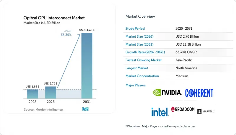
根據 Mordor Intelligence 預測,光 GPU 互連市場規模將從 2025 年的 19.3 億美元和 2026 年的 27 億美元成長到 2031 年的 113.8 億美元,2026 年至 2031 年的複合年成長率為 33.30%。
本報告按產品類型(光收發器、主動光纖等)、互連等級(晶片級、基板級、機架級等)、光纖模式(單模光纖、多模光纖)、資料速率(低於 40 Gbps、40–100 Gbps 等)、應用領域(資料通訊等)和地區進行細分。市場預測以美元計價。
全球光GPU互連市場趨勢與洞察
人工智慧訓練和推理中不斷成長的頻寬需求
到2025年,人工智慧訓練叢集的GPU數量預計將從數千個擴展到數萬個,隨著推理密集模型的日益普及,推理系統也朝著類似的方向發展。這一點意義重大,因為在現代GPU系統中,資料傳輸(而不僅僅是計算本身)現在消耗了很大一部分能源。這種轉變使得互連頻寬成為叢集設計的一個重要限制因素,直接推動了整個光GPU互連市場的需求。圍繞光I/O的行業討論也表明,推理工作負載對低延遲架構的需求日益成長,而這種需求過去主要與訓練環境相關。因此,對光鏈路的需求基礎正在進一步擴大,因為未來對光GPU互連市場的投資不再僅限於訓練最先進的模型。
GPU叢集中銅互連的功率和傳輸距離限制
隨著速度和距離的增加,銅纜鏈路的訊號損耗也會增加,這種物理限制如今正在影響大規模GPU叢集的系統佈局。據NVIDIA稱,在NVL72機架中,NVLink速度下銅纜鏈路的傳輸距離非常短且有限,因此底盤內交換器的放置位置必須受到嚴格限制。隨著系統規模從1個機架擴展到8個機架,光纖通訊正從一個有用的選擇演變為光GPU互連市場的基本需求。發表在《npj Nanophotonics》期刊上的一項研究發現,與光鏈路相比,基於銅纜的擴展網路在達到連貫域極限所需的XPU數量要少得多,這正在改變設計人員對未來叢集規模的思考。電力消耗是促成這種轉變的另一個原因,因為銅纜互連會消耗機架電力,而在光GPU互連市場,營運商更希望將這些電力用於運算。
先進光子封裝和測試高成本
在光GPU互連市場,共封裝光學模組的成本結構遠高於標準插件模組。封裝中CMOS電子元件、矽光電和III-V族材料的組合增加了組裝難度,導致單位成本持續居高不下。測試是另一個問題。矽光電工作流程仍需要從晶圓階段到最終封裝的多個步驟,而這些流程尚未針對大規模生產進行最佳化。此外,光纖和波導管對準所需的高精度使得完全自動化難以實現,導致吞吐量提升速度較之前的收發器週期有所放緩。因此,儘管超大規模資料中心業者已經準備好承擔高昂的初始成本,但光GPU互連市場的企業採用速度仍然緩慢。
細分市場分析
到2025年,光收發器將佔產品類型細分市場的51.47%,在光GPU互連市場中佔據銷售領先地位。這一主導地位歸功於400G和800G插件模組的大規模部署,這些模組已為已部署的AI架構容量提供了支援。這一主導地位清晰地反映了當前部署的成熟度,而非光學整合的長期限制。與新型封裝相比,插件模組更易於理解、擴充性且更易於維護,因此更適合許多短期擴充專案。此外,與高度整合的光封裝相比,插件模組還受益於更成熟的供應鏈。
在機架間鏈路中,主動光纖電纜仍然發揮著至關重要的作用,因為在這些鏈路中,清潔、節能的短距離連接比收發器密度更為重要。此外,光纜組件和光連接器仍然必不可少,因為光GPU互連市場不僅依賴收發器模組本身,還依賴實體光纖佈線、跳線和叢集級安裝層。預計到2031年,嵌入式光學模組的複合年成長率將達到34.29%,使其成為光GPU互連市場中成長最快的產品系列。這種成長反映了從前面板光介面向近封裝和共封裝的轉變,因為集群基數擴展到了銅纜無法實現的規模。 2025年發表在《自然·光子學》上的一項研究也支持了這一趨勢,該研究展示了在類似距離下銅纜無法實現的超低功耗、高頻寬晶片間鏈路。
到 2025 年,基板對板和機架級鏈路將佔互連市場佔有率的 48.84%,成為光纖 GPU 互連市場中最大的細分市場。這一地位反映了乙太網路和 InfiniBand 架構的部署規模,這些架構仍然嚴重依賴大量的機架式光端口。城域和長途分散式互連 (DCI) 位居第二,因為它們提供的是園區和分散式運算站點之間的連接,而不是單一訓練叢集內部的高密度互連架構。儘管如此,隨著人工智慧運算擴展到更多站點以應對電力、冷卻和土地限制,DCI 仍然至關重要。目前,最大的收入來源是正在進行的超大規模建設中需要最多連接埠的領域。
預計到2031年,晶片間互連將以33.89%的最高複合年成長率成長,這預示著光GPU互連市場即將迎來下一個結構性轉變。 Marvell指出,當單通道傳輸速率超過100 Gbps時,被動銅纜的擴展將變得困難,因此光鏈路變得至關重要,即使在機架內部也是如此。 Ayar Labs在OFC 2025上展示了這一發展方向,他們推出了一款UCIe光I/O重定時器晶片,每個光端口的傳輸速率達到1.024 Tbps,每個封裝的傳輸速率達到8.192 Tbps。這些基準測試結果清楚地表明,晶片級光技術為何在光GPU互連市場的長距離產品策略中扮演核心角色。光GPU互連產業正從以基板為中心的擴展模式轉向更加重視光子積體電路設計、晶片整合和先進封裝的模式。
區域分析
2025年,北美佔據了46.32%的光纖GPU互連市場佔有率,持續維持其最大區域收入基礎的地位。這一主導地位得益於Google、微軟、Meta、亞馬遜和其他主要廠商持續大規模擴張人工智慧基礎設施,其規模在其他地區難以匹敵。北美也率先採用了商用CPO技術,NVIDIA的Spectrum-X Photonics乙太網路交換器於2026年5月開始量產,CoreWeave、Lambda和Oracle雲端基礎設施等公司都已成為早期用戶。這種早期採用趨勢使該地區在光纖GPU互連市場中,無論從投資或實際檢驗方面,都擁有了競爭優勢。雖然南美市場規模仍然較小,但隨著超大規模資料中心業者資料中心營運商在巴西和智利擴大資料中心佈局,這兩個國家的重要性日益凸顯。
隨著德國、英國和法國持續擴展其人工智慧訓練和推理能力,歐洲在光纖GPU互連市場保持了顯著佔有率。此外,歐洲企業買家更重視互通性,進一步提升了多廠商標準在增強採購可靠性方面的重要性。 OIF在OFC 2026上對800ZR互通性的現場演示,直接滿足了這一需求,因為該地區的買家往往避免依賴單一廠商的協議棧。雖然中東和非洲仍處於起步階段,但海灣國家主導的人工智慧專案和待開發區專案為直接部署新的800G架構創造了機會,而無需承擔大規模舊有系統升級的負擔。
預計到2031年,亞太地區將以34.27%的複合年成長率成長,成為光GPU互連市場成長最快的地區。該地區憑藉其強大的製造業基礎、先進的光電技術以及公共和私人對人工智慧基礎設施的廣泛投資,佔據了有利地位。日本也因其NTT設立的5億美元光纖網路基金(該基金與人工智慧資料中心基礎設施和更廣泛的全光電戰略相關)而提升了其戰略重要性。韓國和東南亞部分地區也正在崛起為第二大樞紐,進一步拓展了光GPU互連市場的未來收入格局。
其他好處:
- Excel格式的市場預測(ME)表
- 3個月的分析師支持
目錄
第1章:引言
- 研究假設和市場定義
- 調查範圍
第2章:調查方法
第3章執行摘要
第4章 市場狀況
- 市場概覽
- 市場促進因素
- 人工智慧訓練和推理中不斷成長的頻寬需求
- GPU叢集中銅線佈線的功率和佈線距離限制
- 向超大規模資料中心的 800G 和 1.6T 架構過渡
- 下一代GPU平台中採用共封裝光元件
- 主要GPU和交換器廠商的光I/O藍圖
- 用於分散式運算的光纖密度機架式架構
- 市場限制因素
- 先進光子封裝和測試高成本。
- 共封裝設計中的溫度控管限制
- 異質整合中的良率與可靠性挑戰
- 標準化和互通性成熟度的差距
- 宏觀經濟因素對市場的影響
- 產業價值鏈分析
- 監理情勢
- 技術展望
- 波特五力分析
- 價格分析
第5章 市場規模與成長預測
- 依產品類型
- 光收發器
- 主動光纜
- 嵌入式光學模組
- 電纜組件
- 光纖連接器
- 互連等級
- Chip-to-Chip
- 闆對板和機架級
- 城域和遠端DCI
- 光纖模式
- 單模光纖
- 多模光纖
- 按數據速率
- 低於 40 Gbps
- 40~100 Gbps
- 100~400 Gbps
- 超過 400 Gbps
- 透過使用
- 資料通訊
- 電訊
- 按地區
- 北美洲
- 美國
- 加拿大
- 墨西哥
- 歐洲
- 德國
- 英國
- 法國
- 義大利
- 其他歐洲國家
- 亞太地區
- 中國
- 日本
- 韓國
- 印度
- 東南亞
- 其他亞太國家
- 南美洲
- 中東和非洲
- 北美洲
第6章 競爭情勢
- 市場集中度
- 策略趨勢
- Market Positioning Analysis
- 公司簡介
- Broadcom Inc.
- Cisco Systems, Inc.
- NVIDIA Corporation
- Intel Corporation
- Marvell Technology, Inc.
- Coherent Corp.
- Lumentum Holdings Inc.
- Ciena Corporation
- Nokia Corporation
- Infinera Corporation
- Corning Incorporated
- CommScope Holding Company, Inc.
- Amphenol Corporation
- Sumitomo Electric Industries, Ltd.
- Furukawa Electric Co., Ltd.
- TE Connectivity Ltd.
- Ayar Labs, Inc.
- Ranovus Inc.
- Samtec, Inc.
- POET Technologies Inc.
- Innolight Technology Co., Ltd.
第7章 市場機會與未來展望
According to Mordor Intelligence, the optical GPU interconnect market size is projected to expand from USD 1.93 billion in 2025 and USD 2.70 billion in 2026 to USD 11.38 billion by 2031, registering a CAGR of 33.30% between 2026 and 2031.
This report is Segmented by Product Type (Optical Transceivers, Active Optical Cables, and More), Interconnect Level (Chip-To-Chip, Board-To-Board and Rack-Level, and More), Fiber Mode (Single-Mode Fiber, and Multimode Fiber), Data Rate (Less Than 40 Gbps, 40 To 100 Gbps, and More), Application (Data Communication, and More), and Geography. The Market Forecasts are Provided in Terms of Value (USD).
Global Opitcal GPU Interconnect Market Trends and Insights
Rising AI Training and Inference Bandwidth Demand
AI training clusters expanded from thousands to tens of thousands of GPUs through 2025, and inference systems are now moving in the same direction as reasoning-heavy models become more common. This matters because data movement, not computation alone, now consumes much of the energy inside modern GPU systems. That shift makes interconnect bandwidth a practical limit on cluster design, which directly supports demand across the optical GPU interconnect market. Industry discussions around optical I/O also show that inference workloads increasingly need the same low-latency fabric once associated mainly with training deployments. The result is a broader demand base for optical links, as future spending is no longer tied solely to frontier model training in the optical GPU interconnect market.
Copper Interconnect Power and Reach Limits in GPU Clusters
Copper links face rising signal loss as speed and distance increase, and that physical limit is now affecting system layout in large GPU clusters. NVIDIA explained that, in the NVL72 rack, copper runs at NVLink speeds were limited to very short distances, which is why switch placement had to remain tightly constrained inside the chassis. As systems scale from one rack to eight racks, optics move from a useful option to a basic requirement in the optical GPU interconnect market. Research in npj Nanophotonics also found that copper-based scale-up networks cap coherent domains at far lower XPU counts than optical links, which changes how designers think about future cluster size. Power use adds another reason for the shift, because copper-heavy interconnects consume rack power that operators would rather reserve for compute in the optical graphics processing unit (GPU) interconnect market.
High Cost of Advanced Photonic Packaging and Test
The cost profile of co-packaged optics is much higher than that of standard pluggable modules in the optical GPU interconnect market. Packaging combines CMOS electronics, silicon photonics, and III-V materials, making assembly more difficult and keeping unit economics elevated. Testing adds a second problem because silicon photonics workflows still require several insertions from the wafer stage to the final package, and those flows are not yet optimized for very large volumes. Fiber-to-waveguide alignment also demands precision that is hard to automate fully, so throughput gains do not come as quickly as they did in earlier transceiver cycles. This slows broad enterprise adoption in the optical GPU interconnect market even though hyperscalers are already willing to absorb higher early-stage costs.
Other drivers and restraints analyzed in the detailed report include:
- Hyperscale Data Center Migration To 800G and 1.6T Architectures
- Co-Packaged Optics Adoption In Next-Generation GPU Platforms
- Thermal Management Constraints in Co-Packaged Designs
For complete list of drivers and restraints, kindly check the Table Of Contents.
Segment Analysis
Optical Transceivers held 51.47% of the product type segment in 2025, giving them the leading revenue position in the optical GPU interconnect market. Their lead came from the large installed base of pluggable 400G and 800G modules already supporting deployed AI fabric capacity. That dominance says more about the maturity of current deployments than any long-term limit on optical integration. Pluggables still fit many near-term buildouts because they remain familiar, scalable, and easier to service than newer formats. They also continue to benefit from supply chains that are more established than those for deeply integrated optical packages.
Active Optical Cables stayed relevant for rack-to-rack links where transceiver density mattered less than clean, power-aware short-reach connectivity. Cable Assemblies and Optical Connectors also remained essential because the optical GPU interconnect market depends on physical fiber distribution, patching, and cluster-level installation layers, not only on the transceiver module itself. Embedded Optical Modules are projected to grow at a 34.29% CAGR through 2031, which makes them the fastest-growing product group in the optical GPU interconnect market. That growth reflects the shift from front-panel optics to near-package and co-packaged integration as cluster radix expands beyond what copper can handle. A 2025 Nature Photonics study on 3D photonic integration reinforced this direction by showing ultra-low-energy, high-bandwidth interchip links that copper cannot match at similar reach.
Board-to-Board and Rack-Level links held 48.84% of the interconnect segment in 2025, making them the largest current layer in the optical GPU interconnect market. Their position reflected the scale of deployed Ethernet and InfiniBand fabrics that still rely on large volumes of rack-connected optical ports. Metro and Long-Haul DCI occupied a secondary position because they provide connectivity between campuses and distributed compute locations rather than the dense internal fabric within each training cluster. Even so, DCI remains relevant because AI compute is spreading across more sites to manage power, cooling, and land limits. The largest revenue pool today still sits where current hyperscale buildouts require the highest port counts.
Chip-to-Chip is projected to record the fastest CAGR of 33.89% through 2031, signaling the next structural shift in the optical GPU interconnect market. Marvell has argued that passive copper traces stop scaling well beyond 100Gbps per lane, which is why optical links begin to matter even inside a rack. Ayar Labs demonstrated this direction at OFC 2025 with a UCIe Optical I/O Retimer Chiplet that delivered 1.024Tbps per optical port and 8.192Tbps per package. Those benchmarks show why chip-level optics are becoming central to long-range product positioning in the optical GPU interconnect market. The optical GPU interconnect industry is now moving from a board-focused scaling model to one that places more value on photonic IC design, chiplet integration, and advanced packaging.
Complete Report Scope:
- By Product Type
- Optical Transceivers
- Active Optical Cables
- Embedded Optical Modules
- Cable Assemblies
- Optical Connectors
- By Interconnect Level
- Chip-to-Chip
- Board-to-Board and Rack-Level
- Metro and Long-Haul DCI
- By Fiber Mode
- Single-Mode Fiber
- Multimode Fiber
- By Data Rate
- Less Than 40 Gbps
- 40 to 100 Gbps
- 100 to 400 Gbps
- Above 400 Gbps
- By Application
- Data Communication
- Telecommunication
- By Geography
- North America
- United States
- Canada
- Mexico
- Europe
- Germany
- United Kingdom
- France
- Italy
- Rest of Europe
- Asia-Pacific
- China
- Japan
- South Korea
- India
- Southeast Asia
- Rest of Asia-Pacific
- South America
- Middle East and Africa
- North America
Geography Analysis
North America held 46.32% of the optical GPU interconnect market in 2025, maintaining its position as the largest regional revenue base. The region led because Google, Microsoft, Meta, Amazon, and other major operators continued to expand AI infrastructure at a scale not matched elsewhere. North American demand also moved early into commercial CPO adoption, with NVIDIA's Spectrum-X Photonics Ethernet switch entering production in May 2026 and early users including CoreWeave, Lambda, and Oracle Cloud Infrastructure. That early deployment profile gave the region an advantage in both spending and real-world validation across the optical GPU interconnect market. South America remained smaller, but Brazil and Chile grew in importance as hyperscalers expanded their regional data center footprints.
Europe held a meaningful share of the optical GPU interconnect market because Germany, the United Kingdom, and France continued to build AI training and inference capacity. Enterprise buyers in Europe also placed greater emphasis on interoperability, making multi-vendor standards more important to procurement confidence. OIF's live 800ZR interoperability demonstration at OFC 2026 directly addressed that need in a region where buyers often avoid dependence on a single-vendor stack. The Middle East and Africa remained earlier-stage, but sovereign AI programs and greenfield builds in Gulf states created room for direct adoption of newer 800G architectures without the burden of large legacy refresh cycles.
Asia-Pacific is projected to grow at a 34.27% CAGR through 2031, which makes it the fastest-growing geography in the optical GPU interconnect market. The region benefits from manufacturing depth, strong optoelectronics capabilities, and a wider base of public and private investment in AI infrastructure. Japan also gained strategic weight as NTT worked on a USD 500 million optical network fund tied to AI data center infrastructure and its broader all-photonics roadmap. South Korea and parts of Southeast Asia are also emerging as secondary hubs, broadening the future revenue map for the optical graphics processing unit (GPU) interconnect market.
- Broadcom Inc.
- Cisco Systems, Inc.
- NVIDIA Corporation
- Intel Corporation
- Marvell Technology, Inc.
- Coherent Corp.
- Lumentum Holdings Inc.
- Ciena Corporation
- Nokia Corporation
- Infinera Corporation
- Corning Incorporated
- CommScope Holding Company, Inc.
- Amphenol Corporation
- Sumitomo Electric Industries, Ltd.
- Furukawa Electric Co., Ltd.
- TE Connectivity Ltd.
- Ayar Labs, Inc.
- Ranovus Inc.
- Samtec, Inc.
- POET Technologies Inc.
- Innolight Technology Co., Ltd.
Additional Benefits:
- The market estimate (ME) sheet in Excel format
- 3 months of analyst support
TABLE OF CONTENTS
1 INTRODUCTION
- 1.1 Study Assumptions and Market Definition
- 1.2 Scope of the Study
2 RESEARCH METHODOLOGY
3 EXECUTIVE SUMMARY
4 MARKET LANDSCAPE
- 4.1 Market Overview
- 4.2 Market Drivers
- 4.2.1 Rising AI Training and Inference Bandwidth Demand
- 4.2.2 Copper Interconnect Power and Reach Limits in GPU Clusters
- 4.2.3 Hyperscale Data Center Migration to 800G and 1.6T Architectures
- 4.2.4 Co-Packaged Optics Adoption in Next-Generation GPU Platforms
- 4.2.5 Optical I/O Roadmaps from Leading GPU and Switch Vendors
- 4.2.6 Fiber-Dense Rack and Row Architectures for Disaggregated Compute
- 4.3 Market Restraints
- 4.3.1 High Cost of Advanced Photonic Packaging and Test
- 4.3.2 Thermal Management Constraints in Co-Packaged Designs
- 4.3.3 Yield and Reliability Challenges in Heterogeneous Integration
- 4.3.4 Standards and Interoperability Maturity Gaps
- 4.4 Impact of Macroeconomic Factors on the Market
- 4.5 Industry Value Chain Analysis
- 4.6 Regulatory Landscape
- 4.7 Technological Outlook
- 4.8 Porter's Five Forces Analysis
- 4.8.1 Threat of New Entrants
- 4.8.2 Bargaining Power of Suppliers
- 4.8.3 Bargaining Power of Buyers
- 4.8.4 Threat of Substitutes
- 4.8.5 Intensity of Competitive Rivalry
- 4.9 Pricing Analysis
5 MARKET SIZE AND GROWTH FORECASTS (VALUE)
- 5.1 By Product Type
- 5.1.1 Optical Transceivers
- 5.1.2 Active Optical Cables
- 5.1.3 Embedded Optical Modules
- 5.1.4 Cable Assemblies
- 5.1.5 Optical Connectors
- 5.2 By Interconnect Level
- 5.2.1 Chip-to-Chip
- 5.2.2 Board-to-Board and Rack-Level
- 5.2.3 Metro and Long-Haul DCI
- 5.3 By Fiber Mode
- 5.3.1 Single-Mode Fiber
- 5.3.2 Multimode Fiber
- 5.4 By Data Rate
- 5.4.1 Less Than 40 Gbps
- 5.4.2 40 to 100 Gbps
- 5.4.3 100 to 400 Gbps
- 5.4.4 Above 400 Gbps
- 5.5 By Application
- 5.5.1 Data Communication
- 5.5.2 Telecommunication
- 5.6 By Geography
- 5.6.1 North America
- 5.6.1.1 United States
- 5.6.1.2 Canada
- 5.6.1.3 Mexico
- 5.6.2 Europe
- 5.6.2.1 Germany
- 5.6.2.2 United Kingdom
- 5.6.2.3 France
- 5.6.2.4 Italy
- 5.6.2.5 Rest of Europe
- 5.6.3 Asia-Pacific
- 5.6.3.1 China
- 5.6.3.2 Japan
- 5.6.3.3 South Korea
- 5.6.3.4 India
- 5.6.3.5 Southeast Asia
- 5.6.3.6 Rest of Asia-Pacific
- 5.6.4 South America
- 5.6.5 Middle East and Africa
- 5.6.1 North America
6 COMPETITIVE LANDSCAPE
- 6.1 Market Concentration
- 6.2 Strategic Moves
- 6.3 Market Positioning Analysis
- 6.4 Company Profiles (includes Global Level Overview, Market Level Overview, Core Segments, Financials as available, Strategic Information, Market Rank/Share, Products and Services, Recent Developments)
- 6.4.1 Broadcom Inc.
- 6.4.2 Cisco Systems, Inc.
- 6.4.3 NVIDIA Corporation
- 6.4.4 Intel Corporation
- 6.4.5 Marvell Technology, Inc.
- 6.4.6 Coherent Corp.
- 6.4.7 Lumentum Holdings Inc.
- 6.4.8 Ciena Corporation
- 6.4.9 Nokia Corporation
- 6.4.10 Infinera Corporation
- 6.4.11 Corning Incorporated
- 6.4.12 CommScope Holding Company, Inc.
- 6.4.13 Amphenol Corporation
- 6.4.14 Sumitomo Electric Industries, Ltd.
- 6.4.15 Furukawa Electric Co., Ltd.
- 6.4.16 TE Connectivity Ltd.
- 6.4.17 Ayar Labs, Inc.
- 6.4.18 Ranovus Inc.
- 6.4.19 Samtec, Inc.
- 6.4.20 POET Technologies Inc.
- 6.4.21 Innolight Technology Co., Ltd.
7 MARKET OPPORTUNITIES AND FUTURE OUTLOOK
- 7.1 White-Space and Unmet-Need Assessment

 動態可調式模組市場規模、佔有率和成長分析:按模組類型、技術、應用、最終用戶、波長範圍和地區分類-2026-2033年產業預測
 光纖通訊與網路設備市場-2026-2032年全球市場預測
 環路內光纖市場:按類型、應用和地區分類
 2026年全球光無線通訊市場報告2026年全球分組切片網路(SPN)設備市場報告
 光纖通訊和網路設備市場報告:按組件、技術、產業和地區分類(2026-2034 年)2026年全球分組光纖網路設備市場報告
 光纖通訊系統和網路市場分析及預測(至2035年):按類型、產品類型、服務、技術、組件、應用、部署模式、最終用戶和解決方案分類2026年O波段連貫光學全球市場報告2026年全球光正交頻分多工市場報告