

 |
市場調查報告書
商品編碼
2065428
用於GPU和AI加速器的TSV(矽通孔):市場佔有率分析、產業趨勢與統計、成長預測(2026-2031年)Through-Silicon Via (TSV) For GPU And AI Accelerators - Market Share Analysis, Industry Trends & Statistics, Growth Forecasts (2026 - 2031) |
||||||
※ 本網頁內容可能與最新版本有所差異。詳細情況請與我們聯繫。
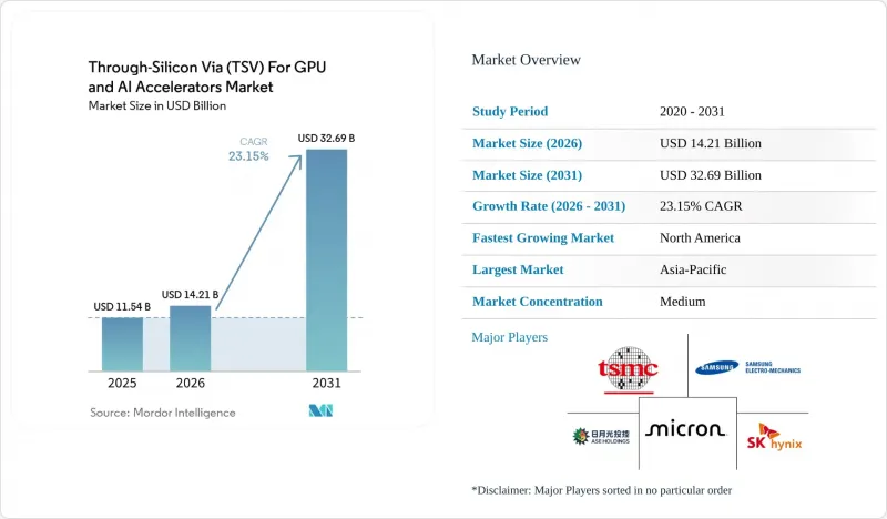
據 Mordor Intelligence 稱,2025 年 GPU 和 AI 加速器的 TSV(矽穿孔電極孔)市場規模為 115.4 億美元,預計到 2031 年將從 2026 年的 142.1 億美元成長至 326.9 億美元,預測期(2026-2031 年)的複合年成長率為 23.15%。
本報告按架構(2.5D TSV(中介層法)、3D TSV(晶片堆疊法))、應用(HBM 記憶體堆疊、GPU 邏輯與記憶體整合、用於 AI 加速器/高效能運算的 GPU、基於晶片組的 GPU 架構)和地區(北美、歐洲、亞太、南美、中東和非洲)進行細分。市場預測以美元(USD)為單位。
全球GPU及AI加速器用TSV(矽通孔)市場趨勢及分析
HBM3及後續技術在AI GPU的主流化應用
HBM3E 和 HBM4 將 TSV 的密度目標提升至每封裝超過 10 萬個通孔,重新定義了封裝的成本結構和製程視窗。 SK 海力士已檢驗了一款 12 層 HBM4 樣品,其頻寬超過 2 Tbit/s,並計劃於 2025 年底開始量產。 NVIDIA 將於 2026 年發布的 Rubin GPU 整合了 288 GB 的 HBM4,並採用了 16 層堆疊結構。這得歸功於三星展示了 12 層 3D-TSV 封裝,其厚度僅為 720µm,與傳統的 8 層 HBM2 相當,因此符合現有伺服器的 Z 軸高度限制。記憶體供應商目前正將基礎晶片邏輯外包給最先進的邏輯代工廠,這提高了對 TSV 對準公差和銅對銅鍵合的要求。隨著供應商競相提供可靠的、高長寬比的通孔,這些變化正在推動 GPU 和 AI 加速器的 TSV(矽通孔)市場快速擴張。
擴展的基於晶片組的GPU設計需要先進的中介層
將單晶片GPU拆分成晶片組可以提高晶片良率並加速產品創新。 AMD的MI300A將5nm計算單元、6nm I/O單元和HBM3整合在單一CoWoS-S中介層上,實現了超過5TB/s的記憶體頻寬。英特爾的Foveros Direct技術支援小於10µm的混合鍵結間距,因此可以垂直堆疊電壓調節器和邏輯層。由三星共同主導的通用晶片互連高速標準(Universal Chiplet Interconnect Express)將於2024年發布開放式的晶片間PHY,使中介層的存取更加解耦。這些進步正在擴大對大型矽中介層的需求,並重振GPU和AI加速器的矽通孔(TSV)市場。
高密度TSV製造的良率挑戰
TSV(矽通孔)的長寬比現已超過10:1,直徑小於5µm,這對蝕刻、填充和曝光製程提出了更高的要求。 IEEE的研究表明,TSV應力會改變電晶體的閾值電壓,因此需要使用禁區來減少矽晶圓的面積。 Chipmetrics的線上空洞檢測技術已識別出熱循環後銅空洞導致的潛在故障。應用材料公司發布了一種等離子濕式TSV曝光模組,該模組可在不損傷銅的情況下去除介電殘留物,從而提高短期良率。在這些措施成熟之前,用於GPU和AI加速器的TSV(矽通孔)的生產仍將繼續受到缺陷密度的限制。
細分市場分析
2.5D TSV中介層憑藉著成熟的設計規則和完善的基板生態系統,預計2025年將佔據GPU和AI加速器TSV(矽通孔)市場68%的佔有率。台積電的CoWoS-S技術支援面積接近2700平方毫米的中介層,能夠在單一基板上容納多個GPU晶片和超過八個HBM立方體。三星的「I-CubeE」技術透過結合矽橋和扇出線路重布,降低了大面積中介層的成本。這些成熟的技術確保了高速流片和可預測的良率,預計在預測期初期,該細分市場將在GPU和AI加速器的TSV(矽通孔)市場中保持其規模。
儘管到2025年,3D晶片堆疊技術僅佔市場佔有率的32%,但由於混合銅鍵合技術能夠實現小於4µm的垂直間距,其複合年成長率(CAGR)高達23.56%。英特爾的「Foveros Direct」和三星的「X-Cube」旨在實現小間距銅-銅連接,從而減少過孔寄生元件並縮短邏輯電路之間的路徑。台積電的SOIC可望實現小於1µm的間距,這將對未來GPU中的SRAM-on-logic堆疊結構大有裨益。隨著元件良率的提高,3D技術與超高頻寬儲存結構結合,可望逐步擴大其在GPU和AI加速器用TSV(矽通孔)領域的市場佔有率。
區域分析
到2025年,亞太地區將主導GPU和AI加速器TSV(矽通孔)市場,佔62%的銷售額。這主要得益於台積電、三星和SK海力士在台灣和韓國的叢集製造、先進封裝和HBM生產。台積電位於日本熊本的研發中心正與基板和材料合作夥伴整合,縮短供應週期,以更新CoWoS藍圖。東京電子已將其2025年的研發投入增加到2,500億日圓(約16.1億美元),以加速鍵合設備的部署並加強區域生態系統。出口限制帶來的不利影響正在限制中國取得先進微影術技術的能力,限制了國內TSV產能,並限制了中國在GPU和AI加速器TSV(矽通孔)市場的佔有率。
北美預計年複合成長率 (CAGR) 為 24.15%,主要受超大規模資料中心業者需求和政府補貼的推動。台積電位於亞利桑那州的多晶矽園區正在為美國本土的 GPU 客戶打造一條 CoWoS 生產線,而安姆科位於皮奧裡亞的工廠則為美國市場帶來了 OSAT(外包半導體製造公司)模式的替代方案。在 CHIPS 法案的支持下,英特爾正在俄亥俄州和亞利桑那州擴張業務,預計這將提高面向國內外市場的 3D 封裝產品的產量。隨著美國資料中心基礎設施投資的增加以及人工智慧加速器成為成長最快的支出類別,國內需求正在進一步擴大。
由於歐盟430億歐元(約464.4億美元)的晶片法案基金,歐洲正在獲得小規模但重要的市場佔有率。本基金用於資助晶圓級鍵結和RDL中介層的試點生產線。義法半導體、環球晶圓代工企業和IMEC正在合作開發一條異質整合測試線,但由於缺乏本地HBM供應,歐洲GPU設計人員仍依賴亞洲記憶體供應商。南美、中東和非洲仍然是次要參與者,僅擁有傳統的後端工藝,缺乏生產TSV(矽通孔裝置)的能力。
其他好處:
- Excel格式的市場預測(ME)表
- 3個月的分析師支持
目錄
第1章:引言
- 市場分析與定義的前提條件
- 分析範圍
第2章 分析方法
第3章執行摘要
第4章 市場狀況
- 市場概覽
- 市場促進因素
- HBM3及後續技術在人工智慧GPU中的主流化
- 擴展的基於晶片組的GPU設計需要先進的中介層
- 2. 增加2.5D/3D包裝設備的資本投入
- 政府對國內半導體供應鏈的支持措施
- 新型混合鍵結TSV技術可提高效能
- 對節能型資料中心加速器的需求日益成長
- 市場限制因素
- 高密度TSV製造的良率挑戰
- 堆疊式GPU模組的溫度控管限制
- 與專用TSV設備相關的供應鏈漏洞
- 替代性先進包裝技術的可用性
- 宏觀經濟因素對市場的影響
- 產業價值鏈分析
- 監理情勢
- 技術展望
- 波特五力分析
第5章:預測市場規模與成長率
- 以建築學為例
- 2.5D TSV(中介層系統)
- 3D TSV(晶片堆疊法)
- 透過使用
- HBM 記憶體堆疊
- GPU邏輯記憶體整合
- 用於高效能運算的人工智慧加速器/GPU
- 基於晶片組的GPU架構
- 按地區
- 北美洲
- 美國
- 加拿大
- 墨西哥
- 歐洲
- 英國
- 德國
- 法國
- 其他歐洲國家
- 亞太地區
- 中國
- 日本
- 印度
- 韓國
- 其他亞太國家
- 南美洲
- 中東和非洲
- 北美洲
第6章 競爭情勢
- 市場集中度
- 策略趨勢
- 市佔率分析
- 公司簡介
- Taiwan Semiconductor Manufacturing Company Limited(TSMC)
- Samsung Electronics Co., Ltd.
- Micron Technology, Inc.
- SK hynix Inc.
- ASE Technology Holding Co., Ltd.
- Intel Corporation
- Amkor Technology, Inc.
- JCET Group Co., Ltd.
- Powertech Technology Inc.
- Siliconware Precision Industries Co., Ltd.
- United Microelectronics Corporation
- GLOBALFOUNDRIES Inc.
- Broadcom, Inc.
- Cadence Design Systems, Inc.
- Synopsys, Inc.
- Lam Research Corporation
- Applied Materials, Inc.
- Tokyo Electron Limited
- Onto Innovation Inc.
- EVG(EV Group)
第7章 市場機會與未來展望
According to Mordor Intelligence, the through-Silicon via for GPU and AI accelerators market size was valued at USD 11.54 billion in 2025 and estimated to grow from USD 14.21 billion in 2026 to reach USD 32.69 billion by 2031, at a CAGR of 23.15% during the forecast period (2026-2031).
This report is Segmented by Architecture (2. 5D TSV Interposer-Based, and 3D TSV Die Stacking), Application (HBM Memory Stacks, GPU Logic-Memory Integration, AI Accelerators and HPC GPUs, and Chiplet-Based GPU Architectures), and Geography (North America, Europe, Asia-Pacific, South America, and Middle East and Africa). The Market Forecasts are Provided in Terms of Value (USD).
Global Through-Silicon Via (TSV) For GPU And AI Accelerators Market Trends and Insights
Mainstream Adoption of HBM3 and Beyond in AI GPUs
HBM3E and HBM4 are lifting TSV density targets above 100,000 vias per package, which redefines packaging cost structures and process windows. SK hynix validated 12-layer HBM4 samples exceeding 2 Tbit-s bandwidth and plans mass production in late 2025. NVIDIA's Rubin GPU, disclosed in 2026, integrates 288 GB of HBM4 and relies on 16-layer stacks that still fit existing server z-height limits because Samsung demonstrated a 12-layer 3D-TSV package that maintains the 720 µm profile of legacy 8-layer HBM2. Memory vendors are now outsourcing base-die logic to leading-edge logic foundries, increasing TSV alignment tolerances and copper-to-copper bonding requirements. These changes are rapidly scaling the Through-Silicon Via market for GPU and AI accelerators as suppliers race to deliver reliable, high-aspect-ratio vias.
Growth of Chiplet-Based GPU Designs Requiring Advanced Interposers
Disaggregating monolithic GPUs into chiplets improves die yield and speeds product refreshes. AMD's MI300A combines 5 nm compute tiles, 6 nm IO tiles, and HBM3 on a single CoWoS-S interposer and delivers over 5 TB-s memory bandwidth. Intel pushed sub-10 µm hybrid-bond pitch with Foveros Direct, enabling vertically stacked voltage regulators and logic layers. The Universal Chiplet Interconnect Express standard, co-led by Samsung, published an open die-to-die PHY in 2024, making interposer access less proprietary. These advances expand demand for large silicon interposers, boosting the Through-Silicon Via market for GPU and AI accelerators.
Yield Challenges in High-Density TSV Fabrication
TSV aspect ratios now exceed 10:1 with diameters below 5 µm, stressing etch, fill, and reveal steps. IEEE research showed that TSV-induced stress shifts transistor thresholds, forcing the use of keep-out zones that erode silicon area. Chipmetrics' inline void detection identified latent failures caused by copper voiding after thermal cycling. Applied Materials released a plasma-wet TSV reveal module that strips dielectric residue without copper damage to raise near-term yields. Until such fixes mature, production output for Through-Silicon Via for GPU and AI accelerators market devices remains gated by defect density.
Other drivers and restraints analyzed in the detailed report include:
- Increasing Capital Investments in 2.5D and 3D Packaging Facilities
- Government Incentives for Domestic Semiconductor Supply Chains
- Thermal Management Limitations in Stacked GPU Modules
For complete list of drivers and restraints, kindly check the Table Of Contents.
Segment Analysis
The 2.5D TSV interposer segment held 68% of the Through-Silicon Via market share for GPU and AI accelerators in 2025, driven by mature design rules and established substrate ecosystems. TSMC's CoWoS-S supports interposers approaching 2,700 mm2, accommodating multiple GPU chiplets and eight or more HBM cubes on one substrate. Samsung's I-CubeE blends silicon bridges with fan-out redistribution layers to lower the cost for large-area interposers. These proven routes ensure high tape-out velocity and predictable yield, sustaining the segment's scale in the Through-Silicon Via market for GPU and AI accelerators during the early forecast years.
3D die-stacking, though only 32% of the 2025 value, is growing at 23.56% CAGR as hybrid copper bonding enables sub-4 µm vertical pitch. Intel's Foveros Direct and Samsung's X-Cube target fine-pitch copper-to-copper joints that trim via parasitics and shorten interlogic paths. TSMC's SoIC promises sub-1 µm pitch, useful for SRAM-on-logic stacks in future GPUs. As equipment yields improve, the 3D route is expected to capture incremental Through-Silicon Via market share for the GPU and AI accelerator market, tied to ultrahigh-bandwidth memory fabrics.
Geography Analysis
Asia-Pacific dominated the Through-Silicon Via for GPU and AI accelerators market in 2025 with a 62% revenue share, driven by TSMC, Samsung, and SK Hynix's cluster fabrication, advanced packaging, and HBM output in Taiwan and South Korea. TSMC's Kumamoto R&D center in Japan co-locates substrate and materials partners, tightening supply cycles for CoWoS roadmap updates. Tokyo Electron scaled 2025 R&D spend to JPY 250.0 billion (USD 1.61 billion) to accelerate the release of bonding equipment and reinforce the regional ecosystem. Export-control headwinds limit China's ability to secure advanced lithography, constraining domestic TSV capacity and limiting its local share of the Through-Silicon Via market for GPU and AI accelerators.
North America's forecast CAGR of 24.15% is driven by hyperscaler demand and government subsidies. TSMC's multi-fab Arizona campus reserves CoWoS lines for U.S. GPU customers, while Amkor's Peoria plant brings an OSAT alternative onshore. Intel's CHIPS-backed Ohio and Arizona expansions promise captive and merchant 3D packaging volumes. The increasing investments in U.S. data-center infrastructure, with AI accelerators emerging as the fastest-growing spend category, are further amplifying domestic demand.
Europe captures a modest but rising share thanks to the EUR 43 billion (approximately USD 46.44 billion) EU Chips Act pool, which finances pilot lines for wafer-level bonding and RDL interposers. STMicroelectronics, GlobalFoundries, and IMEC collaborate on heterogeneous integration test lines, but the absence of a local HBM supply continues to push European GPU designers to Asian memory vendors. South Am, the Middle East End Africa remain marginal, hosting only legacy back-end operations without TSV capacity.
- Taiwan Semiconductor Manufacturing Company Limited (TSMC)
- Samsung Electronics Co., Ltd.
- Micron Technology, Inc.
- SK hynix Inc.
- ASE Technology Holding Co., Ltd.
- Intel Corporation
- Amkor Technology, Inc.
- JCET Group Co., Ltd.
- Powertech Technology Inc.
- Siliconware Precision Industries Co., Ltd.
- United Microelectronics Corporation
- GLOBALFOUNDRIES Inc.
- Broadcom, Inc.
- Cadence Design Systems, Inc.
- Synopsys, Inc.
- Lam Research Corporation
- Applied Materials, Inc.
- Tokyo Electron Limited
- Onto Innovation Inc.
- EVG (EV Group)
Additional Benefits:
- The market estimate (ME) sheet in Excel format
- 3 months of analyst support
TABLE OF CONTENTS
1 INTRODUCTION
- 1.1 Study Assumptions and Market Definition
- 1.2 Scope of the Study
2 RESEARCH METHODOLOGY
3 EXECUTIVE SUMMARY
4 MARKET LANDSCAPE
- 4.1 Market Overview
- 4.2 Market Drivers
- 4.2.1 Mainstream Adoption of HBM3 and Beyond in AI GPUs
- 4.2.2 Growth of Chiplet-Based GPU Designs Requiring Advanced Interposers
- 4.2.3 Increasing Capital Investments in 2.5D/3D Packaging Facilities
- 4.2.4 Government Incentives for Domestic Semiconductor Supply Chains
- 4.2.5 Emerging Hybrid Bonding TSV Techniques for Performance Boost
- 4.2.6 Rising Demand for Energy-Efficient Data Center Accelerators
- 4.3 Market Restraints
- 4.3.1 Yield Challenges in High-Density TSV Fabrication
- 4.3.2 Thermal Management Limitations in Stacked GPU Modules
- 4.3.3 Supply Chain Vulnerabilities to Specialty TSV Equipment
- 4.3.4 Availability of Alternative Advanced Packaging
- 4.4 Impact of Macroeconomic Factors on the Market
- 4.5 Industry Value Chain Analysis
- 4.6 Regulatory Landscape
- 4.7 Technological Outlook
- 4.8 Porter's Five Forces Analysis
- 4.8.1 Bargaining Power of Suppliers
- 4.8.2 Bargaining Power of Buyers
- 4.8.3 Threat of New Entrants
- 4.8.4 Threat of Substitutes
- 4.8.5 Intensity of Competitive Rivalry
5 MARKET SIZE AND GROWTH FORECASTS (VALUE)
- 5.1 By Architecture
- 5.1.1 2.5D TSV (Interposer-based)
- 5.1.2 3D TSV (Die stacking)
- 5.2 By Application
- 5.2.1 HBM Memory Stacks
- 5.2.2 GPU Logic-Memory Integration
- 5.2.3 AI Accelerators / HPC GPUs
- 5.2.4 Chiplet-based GPU Architectures
- 5.3 By Geography
- 5.3.1 North America
- 5.3.1.1 United States
- 5.3.1.2 Canada
- 5.3.1.3 Mexico
- 5.3.2 Europe
- 5.3.2.1 United Kingdom
- 5.3.2.2 Germany
- 5.3.2.3 France
- 5.3.2.4 Rest of Europe
- 5.3.3 Asia-Pacific
- 5.3.3.1 China
- 5.3.3.2 Japan
- 5.3.3.3 India
- 5.3.3.4 South Korea
- 5.3.3.5 Rest of Asia-Pacific
- 5.3.4 South America
- 5.3.5 Middle East and Africa
- 5.3.1 North America
6 COMPETITIVE LANDSCAPE
- 6.1 Market Concentration
- 6.2 Strategic Moves
- 6.3 Market Share Analysis
- 6.4 Company Profiles (includes Global Level Overview, Market Level Overview, Core Segments, Financials as available, Strategic Information, Market Rank/Share, Products and Services, Recent Developments)
- 6.4.1 Taiwan Semiconductor Manufacturing Company Limited (TSMC)
- 6.4.2 Samsung Electronics Co., Ltd.
- 6.4.3 Micron Technology, Inc.
- 6.4.4 SK hynix Inc.
- 6.4.5 ASE Technology Holding Co., Ltd.
- 6.4.6 Intel Corporation
- 6.4.7 Amkor Technology, Inc.
- 6.4.8 JCET Group Co., Ltd.
- 6.4.9 Powertech Technology Inc.
- 6.4.10 Siliconware Precision Industries Co., Ltd.
- 6.4.11 United Microelectronics Corporation
- 6.4.12 GLOBALFOUNDRIES Inc.
- 6.4.13 Broadcom, Inc.
- 6.4.14 Cadence Design Systems, Inc.
- 6.4.15 Synopsys, Inc.
- 6.4.16 Lam Research Corporation
- 6.4.17 Applied Materials, Inc.
- 6.4.18 Tokyo Electron Limited
- 6.4.19 Onto Innovation Inc.
- 6.4.20 EVG (EV Group)
7 MARKET OPPORTUNITIES AND FUTURE OUTLOOK
- 7.1 White-Space and Unmet-Need Assessment
 2.5D 和 3D 半導體封裝市場預測至 2034 年-全球分析(依封裝技術、互連技術、基板類型、材料、晶圓尺寸、應用、最終用戶和地區分類)
 半導體封裝:市場佔有率分析、產業趨勢與統計、成長預測(2026-2031)
 3-D TSV:關鍵問題洞察與市場分析
 高密度封裝(MCM、MCP、SIP、3D-TSV):市場分析與技術趨勢
 2026年全球半導體封裝市場報告
 半導體封裝市場規模、佔有率、趨勢和預測:按類型、封裝材料、技術、最終用戶和地區分類,2026-2034年
 先進晶片封裝市場:依封裝類型和地區分類
 全球防靜電載帶捲市場(按載帶類型、材料、膠帶材料成分、膠帶層數和最終用途產業分類)預測(2026-2032年)導線架固定膠帶市場(按黏合劑類型、背襯材料、膠頻寬度、膠帶厚度、應用、最終用途行業和銷售管道),全球預測,2026-2032年
 MEMS封裝焊料市場規模、佔有率和成長分析:按焊料類型、產品形式、應用、封裝類型、最終用戶和地區分類 - 2026-2033年產業預測