


 |
市場調查報告書
商品編碼
2061513
半導體封裝:市場佔有率分析、產業趨勢與統計、成長預測(2026-2031)Semiconductor Packaging - Market Share Analysis, Industry Trends & Statistics, Growth Forecasts (2026 - 2031) |
||||||
※ 本網頁內容可能與最新版本有所差異。詳細情況請與我們聯繫。
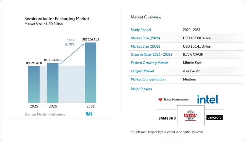
根據 Mordor Intelligence 預測,半導體封裝市場規模預計將在 2025 年達到 954 億美元,2026 年達到 1,030.8 億美元,2031 年達到 1,564.1 億美元,2026 年至 2031 年的複合年成長率為 8.70%。
本報告按封裝平台(先進封裝、傳統封裝)、封裝材料(有機基板、導線架、鍵合線等)、晶圓尺寸(小於200mm、300mm、450mm及以上/片)、經營模式(OSAT、代工廠後端、IDM內部)、用戶產業(家用電子電器等)和地區消費。市場預測以美元計價。
全球半導體封裝市場趨勢及洞察
AI加速器的蓬勃發展正在推動2.5D/3D中介層的發展。
超大規模資料中心營運商目前正在部署每個叢集擁有超過 3 萬個圖形處理器 (GPU) 的叢集,每個集群都依賴高良率的中介層來連接邏輯晶片和高頻寬記憶體堆疊。台積電報告稱,2025 年全年 CoWoS運轉率超過 95%,這使得客戶能夠確保 2027 年的生產檔期。採用 2.5D 製程時,平均良率維持在 75% 左右,這意味著四分之一的基板會被報廢,每個缺陷的成本超過 1 萬美元。英特爾的 Meteor Lake 處理器於 2024 年出貨,實現了 10 微米的凸塊間距,封裝面積減少了 40%,但熱密度接近 200 W/cm²。由於超大規模資料中心業者壟斷了供應,沒有長期合約的小規模無廠半導體公司面臨分配風險。
美國和亞洲的電動車動力組件
電動車逆變器需要能夠承受超過 200 度C結溫以及 150 度C反覆熱循環的動力模組。 Wolfspeed 預計到 2025 年,其 800V 架構的汽車設計採用數量將翻倍,每個逆變器最多可使用 12 個分立模組。 [2] 京瓷和 NGK 火星塞的陶瓷基板導熱係數超過 250 W/m*K,但成本是有機層壓基板的數倍。在美國國內採購獎勵的推動下,英飛凌和安森美半導體已承諾在德克薩斯州和紐約州合計投資 20 億美元用於封裝。同樣,中國垂直整合型企業比亞迪和寧德時代也已將模組組裝納入內部生產,以確保性能和獲利能力。
ABF基板供應短缺(台灣/日本)
2025年全年,味之素的積層製造薄膜(ABF)基板持續供不應求。這是因為IBIDEN和新光電氣的產能擴張計畫要到2026年中期才能全面實現。 12層基板的前置作業時間延長至38週,迫使廠商更改設計並做出效能妥協。一級雲端服務供應商為此投資3億美元在台灣成立合資企業,以確保供應。
細分市場分析
預計到2025年,先進封裝形式將佔據半導體封裝市場65.71%的佔有率,並在2031年之前以10.61%的複合年成長率成長。即使焊料凸塊間距縮小至80µm,覆晶在引腳數較多的裝置中仍佔據主導地位。扇出型晶圓級封裝可將5G射頻前端的組件成本降低20%,而系統級封裝(SiP)和封裝疊層(PoP)架構則最佳化了行動裝置的尺寸。 2.5D/3D子細分市場成長最快,這主要得益於人工智慧加速器在每個中介層中整合八個或更多高頻寬記憶體堆疊。
面板級封裝正逐漸成為一項成本創新技術,預計到2031年將以10.89%的複合年成長率成長。一塊510毫米 x 515毫米的矩形基板可以生產比300毫米晶圓多2.5倍的晶片,從而將單晶片成本降低高達40%。然而,它需要新的處理和檢測工具,並且掌握這項技術需要24個月的時間。傳統的焊線解決方案在電源管理IC、分離式電晶體和傳統汽車應用中仍然發揮著重要作用,因為這些應用領域成本高且認證流程繁瑣。
預計到2025年,有機層壓板將佔據37.82%的市場佔有率,但味之素增材膜的供應限制正在推動設計多樣化。導線架、鍵合線、封裝樹脂和焊球構成了價格敏感型裝置的整體基礎。預計到2025年,銅線的使用率將超過80%,與金線相比,每單位可節省0.02至0.05美元的成本。目前,矽基環氧樹脂模塑材料已被用於承受超過150 度C的汽車級高溫。
受碳化矽 (SiC) 和氮化鎵 (GaN) 功率模組對導熱係數的要求超過 200 W/m*K 的推動,陶瓷封裝預計將以 11.67% 的複合年成長率成長。京瓷透過 2024 年的擴建,將其氮化鋁產能提高了 25%。隨著邏輯功率密度超過 100 W/cm2,晶片黏接和導熱界面材料變得至關重要。在半導體封裝市場,人們持續關注 ABF 介質材料的第二供應商選擇,以避免依賴單一供應商帶來的風險。
區域分析
預計到2025年,亞太地區將佔半導體封裝市場66.89%的佔有率。這主要得益於台灣在覆晶和扇出型封裝製程的領先地位,以及中國在主流組裝領域的規模優勢。然而,自2024年10月起實施的出口限制措施將持續限制中國當地取得先進設備,迫使國內廠商採用混合鍵結等替代方案,以犧牲良率為代價來優先考慮自主生產。韓國的三星和SK海力士已實現記憶體封裝的垂直整合,而日本的信光電氣和IBIDEN在高凸基板製造領域佔據主導地位。
北美市場佔有率正在上升,這主要得益於《晶片封裝法案》(CHIPS Act)的獎勵,這些措施正在推動亞利桑那州、新墨西哥州、德克薩斯州和俄亥俄州新建生產線。安姆科公司在亞利桑那州投資20億美元的工廠以及英特爾不斷擴張的封裝業務,正將先進技術引入該地區,以滿足國防和汽車行業的安全需求。歐洲的規模仍然較小,但預計到2030年,在歐盟《晶片封裝法案》的推動下,其產能將加倍,其中德國德勒斯登叢集主導投資。
中東地區以11.29%的複合年成長率領先全球,主要得益於沙烏地阿拉伯公共投資基金(PIF)和阿拉伯聯合大公國穆巴達拉公司利用石油收入實現半導體業務多元化。計畫於2027-2028年新建的組裝和測試生產線初期將面向消費性電子和汽車模組,隨後拓展至先進中介層。南美和非洲則繼續在細分市場佔有一席之地,專注於焊線和導線架服務,以滿足當地的工業需求。
其他好處:
- Excel格式的市場預測(ME)表
- 3個月的分析師支持
目錄
第1章:引言
- 研究假設和市場定義
- 調查範圍
第2章:調查方法
第3章執行摘要
第4章 市場狀況
- 市場概覽
- 市場促進因素
- AI加速器的蓬勃發展正在推動2.5D/3D中介層的發展。
- 美國和亞洲電動汽車動力組件
- 美國和歐盟的半導體獎勵催生了區域後端晶圓廠。
- 中國和韓國對5G射頻SiP的需求
- 面向物聯網的超低成本面板級封裝
- 支援高密度中介層的晶片組架構
- 市場限制因素
- ABF基板供應短缺(台灣/日本)
- 3D TSV/混合鍵結的良率挑戰
- 對出口至中國的先進封裝設備實施出口限制
- 5nm以下扇出型WLP的散熱限制
- 產業價值鏈分析
- 監理展望
- 宏觀經濟因素對市場的影響
- 技術展望
- 波特五力分析
- 產業產能與投資趨勢分析
- 價格分析
第5章 市場規模與成長預測
- 透過包裝平台
- 先進包裝
- 覆晶
- 扇出 WLP
- WLP風扇
- 2.5D/3D IC
- 嵌入式晶片
- SiP/PoP
- 面板級包裝
- 傳統包裝
- 焊線
- 導線架
- QFN/QFP/SOP
- 先進包裝
- 透過包裝材料
- 有機基板
- 導線架
- 連接線
- 封裝樹脂
- 陶瓷包裝
- 焊球和焊錫凸起
- 晶片黏接和導熱界面材料
- 按晶圓尺寸
- 小於200毫米
- 300 mm
- 超過 450 毫米/面板
- 按經營模式
- OSAT
- 晶圓代工廠後端
- IDM(公司內部)
- 按最終用戶行業分類
- 家用電子產品
- 智慧型手機和穿戴式裝置
- 個人電腦、平板電腦和消費性電子產品
- 計算和資料中心
- 汽車與出行
- 通訊和電信
- 航太/國防
- 醫療和保健設備
- 工業與能源(LED/電力)
- 家用電子產品
- 按地區
- 北美洲
- 美國
- 加拿大
- 墨西哥
- 歐洲
- 德國
- 英國
- 法國
- 其他歐洲國家
- 亞太地區
- 中國
- 日本
- 印度
- 韓國
- 台灣
- 其他亞太國家
- 世界其他地區
- 北美洲
第6章 競爭情勢
- 市場集中度
- 策略趨勢
- 市佔率分析
- 公司簡介
- ASE Technology Holding Co., Ltd.
- Amkor Technology, Inc.
- JCET Group Co., Ltd.
- Siliconware Precision Industries Co., Ltd.
- Powertech Technology Inc.
- Tianshui Huatian Technology Co., Ltd.
- UTAC Holdings Ltd.
- ChipMOS Technologies Inc.
- Chipbond Technology Corp.
- Intel Corporation
- Samsung Electronics Co., Ltd.
- Taiwan Semiconductor Manufacturing Co. Ltd.
- Micron Technology, Inc.
- Texas Instruments Inc.
- Advanced Micro Devices, Inc.
- Hana Micron Inc.
- Nepes Corporation
- TongFu Microelectronics Co., Ltd.
- Shinko Electric Industries Co., Ltd.
- Unisem(M)Berhad
第7章 市場機會與未來展望
According to Mordor Intelligence, the semiconductor packaging market size is projected to be USD 95.40 billion in 2025, USD 103.08 billion in 2026, and reach USD 156.41 billion by 2031, growing at a CAGR of 8.70% from 2026 to 2031.
This report is Segmented by Packaging Platform (Advanced Packaging, Traditional Packaging), Packaging Material (Organic Substrates, Leadframes, Bonding Wires, and More), Wafer Size (Below 200 Mm, 300 Mm, Above 450 Mm/Panel), Business Model (OSAT, Foundry Back-End, IDM In-House), End-User Industry (Consumer Electronics, and More), and Geography. The Market Forecasts are Provided in Terms of Value (USD).
Global Semiconductor Packaging Market Trends and Insights
AI Accelerator Boom Driving 2.5D/3D Interposers
Hyperscale data-center operators now deploy clusters with more than 30,000 graphics processing units per site, each relying on high-yield interposers to connect logic dies to high-bandwidth memory stacks. Throughout 2025, TSMC reported CoWoS capacity utilization above 95%, prompting customers to secure slots through 2027. At 2.5D geometries, average yield hovers near 75%, meaning one in four substrates is scrapped at a cost that can top USD 10,000 per defect. Intel's Meteor Lake processors, shipped in 2024, demonstrated a 10-micron bump pitch, trimming package area by 40% but pushing thermal density toward 200 W/cm2. Smaller fabless firms without long-term contracts face allocation risk as hyperscalers monopolize supply.
Electrified Vehicle Power Packages in the United States and Asia
Electric-vehicle inverters require power modules that survive junction temperatures above 200 °C and repeated 150 °C thermal cycles. Wolfspeed doubled automotive design wins for 800-volt architectures in fiscal 2025, with each inverter consuming up to 12 discrete modules.[2] Ceramic substrates from Kyocera and NGK Spark Plug exhibit thermal conductivities above 250 W/m*K but cost several times more than organic laminates. Domestic-content incentives in the United States prompted Infineon and ON Semiconductor to commit USD 2 billion in packaging investments across Texas and New York. China's vertically integrated BYD and CATL likewise internalized module assembly to secure performance and margin.
ABF Substrate Supply Crunch (Taiwan/Japan)
Ajinomoto Build-up Film substrates remained in short supply during 2025 because capacity expansions at Ibiden and Shinko Electric will not reach volume until mid-2026. Lead times for 12-layer substrates stretched to 38 weeks, forcing redesigns or performance compromises. One tier-1 cloud provider responded by investing USD 300 million in a Taiwanese joint venture to lock in supply.
Other drivers and restraints analyzed in the detailed report include:
- United States and EU CHIPS Incentives Creating Local Back-End Fabs
- Chiplet Architectures Powering High-Density Interposers
- Yield Challenges in 3D TSV/Hybrid Bonding
For complete list of drivers and restraints, kindly check the Table Of Contents.
Segment Analysis
Advanced formats accounted for 65.71% of the semiconductor packaging market share in 2025 and are set to grow at a 10.61% CAGR through 2031. Flip-chip remains dominant for high-pin-count devices as solder-bump pitch tightens to 80 µm. Fan-out wafer-level packaging delivers 20% savings in bill of materials for 5G RF front-ends, while system-in-package and package-on-package architectures optimize mobile footprints. The 2.5D/3D subsegment is the fastest climber, driven by AI accelerators that embed eight or more high-bandwidth memory stacks per interposer.
Panel-level packaging is emerging as a cost disruptor, expected to expand at a 10.89% CAGR through 2031. Rectangular 510 mm X 515 mm substrates yield 2.5 times as many dies as 300 mm wafers, lowering per-die cost by up to 40%. Yet new handling and inspection tools are required, pushing the learning curve to 24 months. Traditional wire-bond solutions preserve relevance in power management ICs, discrete transistors, and legacy automotive applications where cost and qualification inertia dominate.
Organic laminates held a 37.82% share in 2025, but Ajinomoto Build-up Film's supply constraints prompt design diversification. Leadframes, bonding wires, encapsulation resins, and solder balls collectively support price-sensitive devices. Copper wire adoption reached over 80% by 2025, saving USD 0.02-0.05 per unit compared with gold. Epoxy molding compounds now incorporate silicone variants to tolerate automotive temperatures above 150 °C.
Ceramic packages are forecast to grow at an 11.67% CAGR, driven by silicon-carbide and gallium-nitride power modules that require thermal conductivity above 200 W/m*K. Kyocera's 2024 expansion increased aluminum nitride capacity by 25%. Die attach and thermal interface compounds have become critical as logic power density exceeds 100 W/cm2. The semiconductor packaging market continues to scrutinize second-source options for ABF dielectric to avoid single-supplier risk.
Geography Analysis
Asia-Pacific controlled 66.89% of the semiconductor packaging market in 2025, anchored by Taiwan's leadership in flip-chip and fan-out processing and China's scale in mainstream assembly. Export controls enacted in October 2024 continue to limit mainland access to state-of-the-art tools, prompting domestic players to adopt hybrid-bonding workarounds that sacrifice yield for autonomy. South Korea's Samsung and SK Hynix vertically integrate memory packaging, while Japan's Shinko Electric and Ibiden dominate high-layer-count substrate fabrication.
North America's share is rising as CHIPS Act incentives underwrite new lines in Arizona, New Mexico, Texas, and Ohio. Amkor's USD 2-billion plant in Arizona and Intel's packaging expansions bring advanced capability within the region, supporting defense and automotive security requirements. Europe remains smaller but is set to double capacity by 2030 through the EU Chips Act, with Germany's Dresden cluster leading investment.
The Middle East exhibits the fastest regional CAGR at 11.29% as Saudi Arabia's Public Investment Fund and the United Arab Emirates' Mubadala channel oil revenues into semiconductor diversification. Greenfield assembly and test lines scheduled for 2027-2028 will target consumer and automotive modules before progressing to advanced interposers. South America and Africa maintain niche participation, focusing on wire-bond and leadframe services for localized industrial demand.
- ASE Technology Holding Co., Ltd.
- Amkor Technology, Inc.
- JCET Group Co., Ltd.
- Siliconware Precision Industries Co., Ltd.
- Powertech Technology Inc.
- Tianshui Huatian Technology Co., Ltd.
- UTAC Holdings Ltd.
- ChipMOS Technologies Inc.
- Chipbond Technology Corp.
- Intel Corporation
- Samsung Electronics Co., Ltd.
- Taiwan Semiconductor Manufacturing Co. Ltd.
- Micron Technology, Inc.
- Texas Instruments Inc.
- Advanced Micro Devices, Inc.
- Hana Micron Inc.
- Nepes Corporation
- TongFu Microelectronics Co., Ltd.
- Shinko Electric Industries Co., Ltd.
- Unisem (M) Berhad
Additional Benefits:
- The market estimate (ME) sheet in Excel format
- 3 months of analyst support
TABLE OF CONTENTS
1 INTRODUCTION
- 1.1 Study Assumptions and Market Definition
- 1.2 Scope of the Study
2 RESEARCH METHODOLOGY
3 EXECUTIVE SUMMARY
4 MARKET LANDSCAPE
- 4.1 Market Overview
- 4.2 Market Drivers
- 4.2.1 AI Accelerator Boom Driving 2.5D/3D Interposers
- 4.2.2 Electrified Vehicle Power Packages in United States and Asia
- 4.2.3 US-EU CHIPS Incentives Creating Local Back-End Fabs
- 4.2.4 5G RF-SiP Demand in China and Korea
- 4.2.5 Panel Level Packaging for Ultra-Low-Cost IoT
- 4.2.6 Chiplet Architectures Powering High-Density Interposers
- 4.3 Market Restraints
- 4.3.1 ABF Substrate Supply Crunch (Taiwan/Japan)
- 4.3.2 Yield Challenges in 3D TSV/Hybrid Bonding
- 4.3.3 Export Controls on Advanced Packaging Tools to China
- 4.3.4 Thermal Dissipation Limits in Fan-Out WLP at below 5 nm
- 4.4 Industry Value Chain Analysis
- 4.5 Regulatory Outlook
- 4.6 Impact of Macroeconomic Factors on the Market
- 4.7 Technological Outlook
- 4.8 Porter's Five Forces Analysis
- 4.8.1 Bargaining Power of Suppliers
- 4.8.2 Bargaining Power of Buyers
- 4.8.3 Threat of New Entrants
- 4.8.4 Threat of Substitutes
- 4.8.5 Intensity of Competitive Rivalry
- 4.9 Industry Capacity and Investment Trend Analysis
- 4.10 Pricing Analysis
5 MARKET SIZE AND GROWTH FORECASTS (VALUE)
- 5.1 By Packaging Platform
- 5.1.1 Advanced Packaging
- 5.1.1.1 Flip-Chip
- 5.1.1.2 Fan-Out WLP
- 5.1.1.3 Fan-In WLP
- 5.1.1.4 2.5D / 3D IC
- 5.1.1.5 Embedded-Die
- 5.1.1.6 SiP / PoP
- 5.1.1.7 Panel-Level Packaging
- 5.1.2 Traditional Packaging
- 5.1.2.1 Wire-Bond
- 5.1.2.2 Leadframe
- 5.1.2.3 QFN / QFP / SOP
- 5.1.1 Advanced Packaging
- 5.2 By Packaging Material
- 5.2.1 Organic Substrates
- 5.2.2 Leadframes
- 5.2.3 Bonding Wires
- 5.2.4 Encapsulation Resins
- 5.2.5 Ceramic Packages
- 5.2.6 Solder Balls and Bumps
- 5.2.7 Die-Attach and TIMs
- 5.3 By Wafer Size
- 5.3.1 Below 200 mm
- 5.3.2 300 mm
- 5.3.3 Above 450 mm / Panel
- 5.4 By Business Model
- 5.4.1 OSAT
- 5.4.2 Foundry Back-End
- 5.4.3 IDM In-house
- 5.5 By End-user Industry
- 5.5.1 Consumer Electronics
- 5.5.1.1 Smartphones and Wearables
- 5.5.1.2 PCs, Tablets, and Consumer Devices
- 5.5.2 Computing and Data Center
- 5.5.3 Automotive and Mobility
- 5.5.4 Communications and Telecom
- 5.5.5 Aerospace and Defense
- 5.5.6 Medical and Healthcare Devices
- 5.5.7 Industrial and Energy (LED / Power)
- 5.5.1 Consumer Electronics
- 5.6 By Geography
- 5.6.1 North America
- 5.6.1.1 United States
- 5.6.1.2 Canada
- 5.6.1.3 Mexico
- 5.6.2 Europe
- 5.6.2.1 Germany
- 5.6.2.2 United Kingdom
- 5.6.2.3 France
- 5.6.2.4 Rest of Europe
- 5.6.3 Asia-Pacific
- 5.6.3.1 China
- 5.6.3.2 Japan
- 5.6.3.3 India
- 5.6.3.4 South Korea
- 5.6.3.5 Taiwan
- 5.6.3.6 Rest of Asia-Pacific
- 5.6.4 Rest of the World
- 5.6.1 North America
6 COMPETITIVE LANDSCAPE
- 6.1 Market Concentration
- 6.2 Strategic Moves
- 6.3 Market Share Analysis
- 6.4 Company Profiles (includes Global Level Overview, Market Level Overview, Core Segments, Financials as Available, Strategic Information, Market Rank/Share, Products and Services, Recent Developments)
- 6.4.1 ASE Technology Holding Co., Ltd.
- 6.4.2 Amkor Technology, Inc.
- 6.4.3 JCET Group Co., Ltd.
- 6.4.4 Siliconware Precision Industries Co., Ltd.
- 6.4.5 Powertech Technology Inc.
- 6.4.6 Tianshui Huatian Technology Co., Ltd.
- 6.4.7 UTAC Holdings Ltd.
- 6.4.8 ChipMOS Technologies Inc.
- 6.4.9 Chipbond Technology Corp.
- 6.4.10 Intel Corporation
- 6.4.11 Samsung Electronics Co., Ltd.
- 6.4.12 Taiwan Semiconductor Manufacturing Co. Ltd.
- 6.4.13 Micron Technology, Inc.
- 6.4.14 Texas Instruments Inc.
- 6.4.15 Advanced Micro Devices, Inc.
- 6.4.16 Hana Micron Inc.
- 6.4.17 Nepes Corporation
- 6.4.18 TongFu Microelectronics Co., Ltd.
- 6.4.19 Shinko Electric Industries Co., Ltd.
- 6.4.20 Unisem (M) Berhad
7 MARKET OPPORTUNITIES AND FUTURE OUTLOOK
- 7.1 White-Space and Unmet-Need Assessment
 2.5D 和 3D 半導體封裝市場預測至 2034 年-全球分析(依封裝技術、互連技術、基板類型、材料、晶圓尺寸、應用、最終用戶和地區分類)
 用於GPU和AI加速器的TSV(矽通孔):市場佔有率分析、產業趨勢與統計、成長預測(2026-2031年)
 3-D TSV:關鍵問題洞察與市場分析
 高密度封裝(MCM、MCP、SIP、3D-TSV):市場分析與技術趨勢
 2026年全球半導體封裝市場報告
 半導體封裝市場規模、佔有率、趨勢和預測:按類型、封裝材料、技術、最終用戶和地區分類,2026-2034年
 先進晶片封裝市場:依封裝類型和地區分類
 全球防靜電載帶捲市場(按載帶類型、材料、膠帶材料成分、膠帶層數和最終用途產業分類)預測(2026-2032年)導線架固定膠帶市場(按黏合劑類型、背襯材料、膠頻寬度、膠帶厚度、應用、最終用途行業和銷售管道),全球預測,2026-2032年
 MEMS封裝焊料市場規模、佔有率和成長分析:按焊料類型、產品形式、應用、封裝類型、最終用戶和地區分類 - 2026-2033年產業預測