


 |
市場調查報告書
商品編碼
2099754
用於 HBM 的 TSV(矽穿孔電極)技術和設備:市場佔有率分析、行業趨勢和統計數據以及成長預測(2026-2031 年)HBM Through-Silicon Via (TSV) Technology and Equipment - Market Share Analysis, Industry Trends & Statistics, Growth Forecasts (2026 - 2031) |
||||||

※ 本網頁內容可能與最新版本有所差異。詳細情況請與我們聯繫。
據 Mordor Intelligence 稱,用於 HBM 的 TSV(矽穿孔電極)技術和設備的市場規模預計將從 2025 年的 4.5 億美元成長到 2026 年的 5.7 億美元,到 2031 年達到 18.8 億美元,預計 2026 年成長 2031 年的複合年成長率為 26.96%。
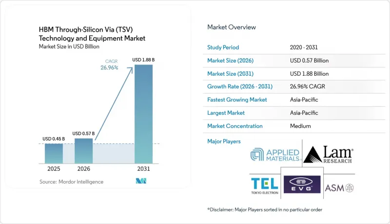
本報告按產品(設備等)、TSV製程類型(通孔優先TSV等)、鍵結技術(直接銅鍵合等)、應用(AI加速器等)、最終用戶(OSAT等)、晶圓尺寸(200毫米等)、整合方式(晶圓間整合等)及地區進行細分。市場預測以美元計價。
全球市場趨勢及對 HBM 用 TSV(矽穿孔電極)技術與設備的洞察。
提高人工智慧加速器中HBM堆疊密度
目前,所有主流人工智慧運算程式都依賴HBM,這使得TSV效能成為最先進加速器封裝的直接供應瓶頸。 HBM4藍圖的目標是每腳頻寬12-16 Gbps,每堆疊1.5-2.0 TB/s,堆疊16層時容量高達128 GB,這持續對通孔中間整合、蝕刻控制和堆疊良率提出挑戰。三星電子已確認將於2026年6月開始出貨商用HBM4內存,顯示下一個生產週期已進入實際供貨階段。隨著堆疊高度的增加,HBM的TSV(矽穿孔電極)技術和設備市場必須適應更薄的晶片、更嚴格的對準、更潔淨的銅填充以及每層更可重複的鍵合視窗。因此,資本投資仍主要集中在設備方面,因為TSV或鍵結階段的良率目標一旦達不到,不僅會降低單一製程步驟的生產速度,還會影響整個記憶體堆疊的生產速度。因此,HBM 的 TSV(矽穿孔電極)技術和設備市場正隨著 AI 的需求而成長,但其製造條件比以往的 HBM 世代更加嚴格。
從 HBM4 和後來的微凸塊過渡到混合鍵結
從基於微凸塊的互連到混合鍵結的轉變,正在改變供應商規劃其下一輪設備週期的方式,即便大規模量產部署尚未成為標準。根據《電子學》雜誌2025年的一篇評論文章,與MR-MUF相比,Cu-Cu混合鍵合可將結處的導熱係數降低20%,並在更小的間距下改善I/O電阻和電容。 2026年6月,三星電子宣布計畫從16層HBM4E開始採用混合銅鍵合技術,並進一步過渡到HBM5。這為設備基礎設施的發展指明了方向,儘管具體時間會因客戶專案而異。此外,2026年5月,Imec和EV Group成功展示了200奈米銅線間距的晶圓間混合鍵合,證實了該技術正朝著超高密度佈線結構的方向發展。這正在為HBM的TSV(矽穿孔電極)技術和設備市場創造兩種截然不同的需求模式。雖然熱壓設備目前仍至關重要,但混合鍵結設備、表面處理系統及相關材料目前正處於認證和生產線規劃階段。這段重疊時期至關重要,因為儘早獲得認證名額的供應商可以在大規模生產真正開始之前很久就對未來的製程標準產生影響。
端到端的TSV工具鏈需要大量的資金投入。
進入用於HBM的TSV(矽穿孔電極)技術和設備市場仍然充滿挑戰。這是因為HBM級生產線需要一整組先進設備,而不僅僅是單一的瓶頸裝置。應用材料公司於2026年6月發布的產品線涵蓋了TSV曝光、銅電鍍、介質沉積和先進檢測等工藝,這表明,一條具有競爭力的生產線必須同時投資多個工藝層。 EV集團和SUSS MicroTec也在2025年和2026年繼續擴展其鍵合和晶片到晶圓平台產品,這凸顯了任何想要支援現代HBM組裝的參與企業都不能依賴有限的設備配置。這些廣泛的要求使得整個生產線的總投資金額達到了只有少數記憶體製造商、代工廠和頂級封裝專家能夠勝任的水平。時機決策也更加困難,因為客戶必須在混合鍵合技術從認證階段過渡到量產階段的速度完全明朗之前就投入資金。限制因素不僅限於資金規模。也存在投資於不合適的下一代本生物管理工具組合的風險。
細分市場分析
2025年,設備部門的銷售額佔總銷售額的77.12%,大部分支出仍集中在設備基礎設施上,這些基礎設施支援整個生產流程中的蝕刻、填充、減薄、鍵結和檢測等工序。從銷售角度來看,這種情況反映出,用於HBM的TSV(矽穿孔電極)技術和設備市場仍然依賴每個製程步驟的高度專業化,難以實現商品化。 2026年6月,應用材料公司宣布預計2026年封裝銷售額將超過20億美元,並推出了Opta Quad CMP平台、Nokota VMax 2 ECD和Producer Avila 2 PECVD,以支援TSV曝光、銅電鍍和介質沉積。這項公告清楚地表明,設備領域的領先地位並非基於單一的設備類別,而是基於能夠以高度整合的效能涵蓋多個高良率製程步驟。設備領域的統治地位也解釋了為什麼新的生產力計畫容易受到前置作業時間。因為即使缺少一件關鍵設備,也可能會延遲全面量產的開始。
材料領域是成長最快的領域,到2031年複合年成長率將達到27.56%,顯示製程複雜性正在轉變。隨著通孔尺寸向更精細的關鍵尺寸發展,鍵合條件也變得更加嚴格,材料在熱穩定性、銅純度、表面處理和瞬態鍵合性能方面的作用日益重要。雖然這種轉變並未取代設備的核心作用,但它提升了能夠在更嚴格的工藝窗口下穩定良率的專用耗材的價值。服務在矽穿孔電極孔(TSV)技術和設備市場(用於HBM)中仍然佔據最小的佔有率,但隨著供應商除了交付設備外,還提供製程最佳化、整合支援和良率提升服務,其重要性正在不斷提升。這點意義重大,因為來自客戶現場的實務經驗會透過服務回饋到供應商生態系統中,進而影響未來的採購決策。因此,儘管目前的產品和服務仍然以設備為中心,但正在逐步向更平衡的模式轉變,在這種模式下,設備、材料和整合支援相互補充。
到2025年,「中間通孔」製程將佔總銷售額的62.52%,這表明用於HBM的TSV(矽穿孔電極)技術和設備市場仍然以已整合到商業HBM製造中的製程架構為中心。預計到2031年,該細分市場將以27.51%的複合年成長率成長,這意味著成長是由同一製程平台上產能的提升驅動,而不是向不同TSV製程序列的廣泛轉變。根據2025年未來儲存大會的資料,主要的HBM供應商正在大規模生產中標準化「中間通孔」工藝,這解釋了為什麼其應用基礎仍然穩固。這種標準化至關重要,因為它不僅確定了製程選擇,還確定了相關的工具組合、操作人員的專業知識和良率最佳化流程。一旦這些要素成熟,除非新方法在成本、密度或可靠性方面具有極其明顯的優勢,否則客戶將不願輕易轉換製程。
在一些應用場景較為有限的領域,「通孔優先」仍然十分重要,因為在這些領域,必須在後續製程之前建立晶圓間的連接,這種趨勢在HBM主要量產基地以外的地區尤為明顯。 「通孔後置」在中介層和某些異質整合領域仍然發揮作用,因為在這些領域,製程柔軟性比記憶體堆疊所需的高密度垂直間距更為重要。由於HBM的生產仍佔據最大的商業產量,因此這兩種方案在短期內都不足以取代「通孔中間」方案。因此,HBM TSV(矽穿孔電極)技術和設備市場的製程創新通常是在「通孔中間」框架內進行的,而不是在其之外進行的。因此,供應商之間的競爭並非在於替換整個架構,而是改進蝕刻輪廓控制、銅填充品質、晶圓減薄穩定性以及下游製程的鍵結相容性。因此,儘管市場銷售看起來充滿活力,但支撐其大部分成長的工藝路徑在結構上卻是保守的。
預計到2025年,熱壓鍵合將佔銷售額的69.74%,繼續保持其最大的應用基礎,為HBM2E到HBM3E的生產提供支持,並在當前的供應中發揮核心作用。這一佔有率表明,HBM TSV(矽穿孔電極)技術和設備市場仍然依賴具有成熟商業性量產記錄的製程穩定性。混合鍵結是成長最快的技術,到2031年複合年成長率將達到27.76%,反映了高層記憶體堆疊中更小間距和更低熱阻的發展趨勢。 《2025年電子展望》概述了混合鍵結為何對未來的HBM設計具有吸引力,尤其是在隨著間距小型化而需要提高熱性能和電氣性能的情況下。此外,三星電子已確認在16層HBM4E及更高層級產品中採用混合銅鍵合的藍圖,為該領域提供了清晰的商業性指南,即使過渡並非一蹴而就。
現有的熱壓技術仍然至關重要,因為許多短期HBM生產無法等到完全過渡到混合鍵合技術。因此,HBM的TSV(矽穿孔電極)技術和設備市場並沒有明顯的更新換代週期,兩種技術在不同的生產週期中都將繼續發揮重要作用。根據BESI的一份報告,2026年第一季的訂單年增104.5%,顯示眾多客戶對混合鍵結技術的需求。這表明認證活動已經轉化為實際的資本投資。此外,Imec和EV Group的200奈米晶圓間演示表明,如果製程針對未來的整合密度進行最佳化,間距小型化的可能性將非常大。雖然微凸塊和直接銅纜鍵合技術仍發揮有限的作用,但目前主要的競爭挑戰在於,哪些供應商既能滿足當前對熱壓技術的需求,又能確保其在未來混合鍵結技術中的地位。這種平衡將決定哪些供應商能夠在記憶體堆疊層數超過當前水準後繼續保持市場主導地位。
區域分析
預計到2025年,亞太地區將佔據HBM(矽穿孔電極)技術和設備市場77.83%的佔有率,並將在2031年之前以27.94%的複合年成長率持續成長。這一雙重地位反映了該地區正在將記憶體生產、代工封裝、OSAT(外包半導體組裝和測試)支援以及設備供應整合到一個互聯互通的中心。韓國仍然是該地區的核心,三星電子和SK海力士引領HBM的商業化生產,韓國透過有針對性的公共支援不斷增強其封裝能力。台灣憑藉其代工和OSAT基地,正在鞏固其在該地區的地位,這些基地支援與人工智慧運算專案相關的各種先進封裝需求。日本作為設備和製程生態系統的重要貢獻者,使亞太地區不僅在產量方面,而且在設備可用性和生產基礎設施發展方面都保持著優勢。
儘管預計北美在2025年的市佔率相對較小,但其作為矽穿孔電極(TSV)技術和HBM設備市場資金、設備和未來封裝產能中心的重要性日益凸顯。 2025年1月,美國政府獲得了14億美元的CHIPS封裝支援津貼,為該地區的原型開發、試生產和製程開發奠定了更堅實的基礎。類似的政策支持也為SK海力士在印第安納州的計畫提供了高達4.58億美元的資金,將公共支持與美國未來HBM封裝產能的建設聯繫起來。 KLA預計其先進封裝相關銷售額將從2025年的約6.35億美元成長到2026年的約10億美元,顯示北美設備製造商正從這項設備擴張週期中獲益。
2025年,歐洲仍將維持以供應商主導的專業化角色,而非大規模的HBM生產線。 SUSS MicroTec和EV集團仍然是該地區鍵合和整合設備領域的領導企業,並在2025年和2026年積極發布產品和技術公告。儘管歐洲的製造規模小於亞太地區,但這仍確立了歐洲在HBM TSV(矽穿孔電極)技術和設備市場的重要技術地位。南美、中東和非洲仍處於起步階段,直接參與TSV生產的程度有限,它們作為人工智慧硬體的下游用戶的重要性日益凸顯,而非HBM封裝能力的核心來源。
其他好處:
- Excel格式的市場預測(ME)表
- 3個月的分析師支持
目錄
第1章:引言
- 研究假設和市場定義
- 調查範圍
第2章:調查方法
第3章執行摘要
第4章 市場狀況
- 市場概覽
- 宏觀經濟因素對市場的影響
- 市場促進因素
- 提高人工智慧加速器的HBM堆疊密度
- HBM4及後續技術中從微凸塊到混合鍵結的過渡
- 晶圓代工廠和OSAT工廠提高了先進封裝的產能。
- 國內半導體補貼用於先進封裝設備的發展
- 高深長寬比TSV蝕刻和填充的良率學習曲線
- 引入即時測量和製程線上控制
- 市場限制因素
- 對端對端TSV工具鏈的高額資本投入
- 禁入區的熱應力與設計限制
- 高密度填充和暴露製程中產量降低的風險。
- 多供應商 HBM 供應鏈中工具認證的複雜性
- 供應鏈分析
- 監理情勢
- 技術展望
- 波特五力分析
第5章 市場規模與成長預測
- 報價
- 裝置
- 材料
- 服務
- TSV製程類型
- 啤酒優先 TSV
- 啤酒中級TSV
- 透過 Rust Type TSV
- 鍵合技術
- 熱壓黏接
- 混合鍵合
- 微凸塊黏合
- 直接銅纜鍵合
- 透過使用
- 高頻寬內存
- 人工智慧加速器
- GPU 封裝
- 高效能運算處理器
- 基於晶片組的處理器
- 其他先進封裝應用
- 最終用戶
- 記憶體製造商
- 鑄造廠
- 垂直整合設備製造商(IDM)
- OSAT
- 研究機構
- 按晶圓尺寸
- 200 mm
- 300 mm
- 其他晶圓尺寸
- 透過整合
- 晶圓之間
- 從晶片到晶圓
- 死而復生
- 按地區
- 北美洲
- 美國
- 加拿大
- 墨西哥
- 歐洲
- 德國
- 英國
- 法國
- 義大利
- 其他歐洲國家
- 亞太地區
- 中國
- 日本
- 韓國
- 台灣
- 印度
- 其他亞太國家
- 南美洲
- 中東和非洲
- 北美洲
第6章 競爭情勢
- 市場集中度
- 策略趨勢
- 市佔率分析
- 公司簡介
- Applied Materials, Inc.
- Lam Research Corporation
- Tokyo Electron Limited
- EV Group
- ASM International NV
- BESI
- Hanmi Semiconductor Co., Ltd.
- SEMES Co., Ltd.
- SK hynix Inc.
- Samsung Electronics Co., Ltd.
- Micron Technology, Inc.
- Taiwan Semiconductor Manufacturing Company Limited
- Intel Corporation
- Amkor Technology, Inc.
- ASE Technology Holding Co., Ltd.
- Powertech Technology Inc.
- Siliconware Precision Industries Co., Ltd.
- JCET Group Co., Ltd.
- Onto Innovation Inc.
- KLA Corporation
- SCREEN Holdings Co., Ltd.
- DISCO Corporation
- Plasma-Therm
- Cohu, Inc.
- SUSS MicroTec SE
- Shinkawa Ltd.
- Brewer Science, Inc.
第7章 市場機會與未來展望
According to Mordor Intelligence, the HBM through-Silicon via (TSV) technology and equipment market size is expected to increase from USD 0.45 billion in 2025 to USD 0.57 billion in 2026 and reach USD 1.88 billion by 2031, growing at a CAGR of 26.96% over 2026-2031.
This report is Segmented by Offering (Equipment, and More), TSV Process Type (Via-First TSV, and More), Bonding Technology (Direct Copper Bonding, and More), Application (AI Accelerators, and More), End User (OSATs, and More), Wafer Size (200 Mm, and More), Integration (Wafer-To-Wafer, and More), and Geography. The Market Forecasts are Provided in Terms of Value (USD).
Global HBM Through-Silicon Via (TSV) Technology and Equipment Market Trends and Insights
AI Accelerator HBM Stack Density Expansion
Every major AI compute program now depends on HBM, so TSV performance has become a direct supply constraint for advanced accelerator packages. The HBM4 roadmap targets 12-16 Gbps per pin, 1.5-2.0 TB/s bandwidth per stack, and up to 128 GB through 16-layer stacking, which keeps pressure on via-middle integration, etch control, and stacking yield. Samsung Electronics confirmed in June 2026 that it had shipped commercial HBM4 memory, which shows that the next production cycle has already moved into live customer supply. As stack height rises, the HBM Through-Silicon Via (TSV) technology and equipment market must support thinner dies, tighter alignment, cleaner copper fill, and more repeatable bonding windows across each layer. That is why capacity spending remains front-loaded into tools, because a missed yield target at the TSV or bonding stage can slow the output of the full memory stack rather than a single process step. The result is that the HBM Through-Silicon Via (TSV) technology and equipment market is growing in line with AI demand, but it is doing so under harder manufacturing conditions than earlier HBM generations.
Transition From Microbump to Hybrid Bonding in HBM4 and Beyond
The shift from microbump-based interconnects to hybrid bonding is changing how vendors plan the next equipment cycle, even before full volume adoption becomes standard. A 2025 review in Electronics reported that Cu-Cu hybrid bonding can lower joint thermal resistance by 20% versus MR-MUF while also improving I/O resistance and capacitance at finer pitch. Samsung Electronics stated in June 2026 that it plans to use hybrid copper bonding from 16-layer HBM4E and then move further with HBM5, which gives the equipment base a clear direction even if the timing remains staggered by customer program. Imec and EV Group also demonstrated wafer-to-wafer hybrid bonding at 200 nm Cu interconnect pitch in May 2026, which confirms that the technology path is advancing toward very fine interconnect density. For the HBM Through-Silicon Via (TSV) technology and equipment market, this creates a two-speed demand pattern where thermocompression tools remain essential now, while hybrid bonding tools, surface preparation systems, and related materials move through qualification and line planning. That overlap matters because suppliers that win early qualification slots can influence future process standards long before high-volume ramps start.
High Capex for End-To-End TSV Toolchains
The HBM Through-Silicon Via (TSV) technology and equipment market remains difficult to enter because an HBM-grade line needs a full set of advanced tools rather than a single bottleneck machine. Applied Materials' June 2026 launch covered TSV reveal, copper plating, dielectric deposition, and advanced inspection, which shows how many process layers must be funded together before a line becomes competitive. EV Group and SUSS MicroTec also continued to expand bonding and die-to-wafer platforms in 2025 and 2026, which underlines that no entrant can rely on a narrow tool footprint if it wants to support modern HBM assembly. That broad requirement pushes total line spending into a level that only a few memory makers, foundries, and top-tier packaging specialists can manage with confidence. It also makes timing more difficult, because customers must commit capital before it is fully clear how quickly hybrid bonding will move from qualification into large-scale production. The restraint is not just the size of the check, it is the risk of funding the wrong mix of tools for the next HBM generation.
Other drivers and restraints analyzed in the detailed report include:
- Advanced Packaging Capacity Additions by Foundries and OSATs
- Domestic Semiconductor Subsidies for Advanced Packaging Buildouts
- Thermal Stress and Keep-Out Zone Design Constraints
For complete list of drivers and restraints, kindly check the Table Of Contents.
Segment Analysis
Equipment held 77.12% of revenue in 2025, which kept the largest share of spending concentrated in the tool base that enables etch, fill, thinning, bonding, and inspection across the production flow. In revenue terms, that position reflects how the HBM Through-Silicon Via (TSV) technology and equipment market still depends on each process step being too specialized to commoditize. Applied Materials said in June 2026 that it expects packaging revenue to exceed USD 2 billion in 2026 and introduced the Opta Quad CMP platform, Nokota VMax 2 ECD, and Producer Avila 2 PECVD to support TSV reveal, copper plating, and dielectric deposition. That launch makes clear that equipment leadership is not based on one machine category, but on the ability to cover multiple high-yield process steps with tightly integrated performance. The dominance of equipment also shows why new capacity plans remain vulnerable to lead times, because missing one critical tool can delay a full production ramp.
Materials are the fastest-growing offering at a 27.56% CAGR through 2031, which signals a change in where process difficulty is starting to migrate. As via dimensions move toward finer critical dimensions and bonding conditions become stricter, materials now carry more of the burden for thermal stability, copper purity, surface preparation, and temporary bonding performance. That shift does not remove the central role of tools, but it raises the value of specialized consumables that can stabilize yield under more aggressive process windows. Services remain the smallest part of the HBM Through-Silicon Via (TSV) technology and equipment market, yet they are becoming more important as vendors provide process tuning, integration support, and yield improvement work alongside equipment delivery. This matters because services can move practical know-how from the customer floor back into the vendor ecosystem, which can shape later buying decisions. The offering mix therefore still favors tools today, but it is slowly moving toward a more balanced model where equipment, materials, and integration support reinforce one another.
Via-middle captured 62.52% of process-type revenue in 2025, which shows that the HBM Through-Silicon Via (TSV) technology and equipment market remains centered on the process architecture already embedded in commercial HBM manufacturing. The same segment is projected to expand at a 27.51% CAGR through 2031, which means growth is coming from more capacity on the same process foundation rather than from a broad shift into a different TSV sequence. Future Memory Storage Conference material from 2025 showed that major HBM suppliers have standardized on via-middle TSV in production, which explains why its installed base remains strong. That standardization matters because it locks in not only process preference, but also the surrounding tool stack, operator know-how, and yield optimization routines. Once those elements are mature, customers become less willing to switch unless a new method offers a very clear gain in cost, density, or reliability.
Via-first remains relevant in narrower use cases where through-wafer connectivity must be built before later processing, especially in areas outside the main HBM volume base. Via-last still has a place in interposer and selected heterogeneous integration work where process flexibility can matter more than the dense vertical pitch needed in memory stacking. Neither of those routes has enough current pull to displace via-middle in the near term, because HBM production is where the largest commercial volumes continue to sit. This leaves the HBM Through-Silicon Via (TSV) technology and equipment market in a position where process innovation must often happen inside the via-middle framework rather than outside it. Vendors therefore compete by improving etch profile control, copper fill quality, wafer thinning stability, and downstream bonding compatibility instead of trying to replace the full architecture. The result is a market that looks dynamic from a revenue perspective, but structurally conservative in the process path that supports most of that growth.
Thermocompression bonding held 69.74% of revenue in 2025, which kept the largest installed base aligned with the method that has supported HBM2E through HBM3E production and remains central to current supply. That share shows how the HBM Through-Silicon Via (TSV) technology and equipment market still relies on process stability where commercial volume is already proven. Hybrid bonding is the fastest-growing technology at a 27.76% CAGR through 2031, reflecting the push toward finer pitch and lower thermal resistance in taller memory stacks. The 2025 Electronics review outlined why hybrid bonding is attractive for future HBM designs, especially where improved thermal and electrical performance becomes necessary at smaller pitch. Samsung Electronics also confirmed a roadmap that uses hybrid copper bonding from 16-layer HBM4E onward, which gives the segment a defined commercial direction even if the transition will not happen in one step.
The installed thermocompression base still matters because most near-term HBM output cannot wait for full hybrid conversion. That is why the HBM Through-Silicon Via (TSV) technology and equipment market is not seeing a clean replacement cycle, but a period where both technologies stay important for different production windows. BESI reported that Q1 2026 orders rose 104.5% year over year with hybrid bonding demand from multiple customers, which suggests that qualification activity is already translating into real capital commitments. Imec and EV Group's 200 nm wafer-to-wafer demonstration also shows how far pitch scaling can go when the process is optimized for future integration density. Micro-bump and direct copper bonding still serve narrower roles, but the main competitive question now is which vendors can support present thermocompression needs while securing future hybrid bonding positions. That balance is likely to decide which suppliers stay embedded when memory stacks move beyond current layer counts.
Complete Report Scope:
- By Offering
- Equipment
- Materials
- Services
- By TSV Process Type
- Via-First TSV
- Via-Middle TSV
- Via-Last TSV
- By Bonding Technology
- Thermocompression Bonding
- Hybrid Bonding
- Micro-Bump Bonding
- Direct Copper Bonding
- By Application
- High Bandwidth Memory
- AI Accelerators
- GPU Packages
- HPC Processors
- Chiplet-Based Processors
- Other Advanced Packaging Applications
- By End User
- Memory Manufacturers
- Foundries
- Integrated Device Manufacturers (IDMs)
- OSATs
- Research Institutes
- By Wafer Size
- 200 mm
- 300 mm
- Other Wafer Sizes
- By Integration
- Wafer-to-Wafer
- Die-to-Wafer
- Die-to-Die
- By Geography
- North America
- United States
- Canada
- Mexico
- Europe
- Germany
- United Kingdom
- France
- Italy
- Rest of Europe
- Asia-Pacific
- China
- Japan
- South Korea
- Taiwan
- India
- Rest of Asia-Pacific
- South America
- Middle East and Africa
- North America
Geography Analysis
Asia-Pacific held 77.83% of the HBM Through-Silicon Via (TSV) technology and equipment market share in 2025 and is projected to expand at a 27.94% CAGR through 2031. That dual position reflects the fact that the region combines memory production, foundry packaging, OSAT support, and equipment supply in one interconnected footprint. South Korea remains central because Samsung Electronics and SK hynix anchor commercial HBM output, and the country also continues to back packaging capability through targeted public support. Taiwan strengthens the regional position through its foundry and OSAT base, which supports broader advanced packaging demand tied to AI compute programs. Japan remains important as an equipment and process ecosystem contributor, which helps keep Asia-Pacific ahead not only in output but also in tool availability and production readiness.
North America held a smaller position in 2025, but it is becoming more important as a funding, equipment, and future packaging capacity base for the HBM Through-Silicon Via (TSV) technology and equipment market. The U.S. government finalized USD 1.4 billion in CHIPS packaging awards in January 2025, which gave the region a stronger platform for prototyping, pilot production, and process development. The same policy direction supported up to USD 458 million for SK hynix's Indiana project, linking public support to future HBM packaging capability inside the United States. KLA said its advanced packaging revenue was expected to rise from around USD 635 million in 2025 to around USD 1 billion in 2026, which shows how North American toolmakers are capturing value from this buildout cycle.
Europe maintained a specialized role in 2025, led by equipment vendors rather than large-scale HBM production lines. SUSS MicroTec and EV Group remain the main regional names in bonding and integration tools, and both stayed active in 2025 and 2026 through product and technology announcements. This gives Europe an important technical position inside the HBM Through-Silicon Via (TSV) technology and equipment market even though its manufacturing base is narrower than Asia-Pacific's. South America and the Middle East and Africa remained at an early stage, with limited direct participation in TSV production and stronger relevance as downstream users of AI hardware than as core sources of HBM packaging capacity.
- Applied Materials, Inc.
- Lam Research Corporation
- Tokyo Electron Limited
- EV Group
- ASM International N.V.
- BESI
- Hanmi Semiconductor Co., Ltd.
- SEMES Co., Ltd.
- SK hynix Inc.
- Samsung Electronics Co., Ltd.
- Micron Technology, Inc.
- Taiwan Semiconductor Manufacturing Company Limited
- Intel Corporation
- Amkor Technology, Inc.
- ASE Technology Holding Co., Ltd.
- Powertech Technology Inc.
- Siliconware Precision Industries Co., Ltd.
- JCET Group Co., Ltd.
- Onto Innovation Inc.
- KLA Corporation
- SCREEN Holdings Co., Ltd.
- DISCO Corporation
- Plasma-Therm
- Cohu, Inc.
- SUSS MicroTec SE
- Shinkawa Ltd.
- Brewer Science, Inc.
Additional Benefits:
- The market estimate (ME) sheet in Excel format
- 3 months of analyst support
TABLE OF CONTENTS
1 INTRODUCTION
- 1.1 Study Assumptions and Market Definition
- 1.2 Scope of the Study
2 RESEARCH METHODOLOGY
3 EXECUTIVE SUMMARY
4 MARKET LANDSCAPE
- 4.1 Market Overview
- 4.2 Impact of Macroeconomic Factors on the Market
- 4.3 Market Drivers
- 4.3.1 AI Accelerator HBM Stack Density Expansion
- 4.3.2 Transition From Microbump to Hybrid Bonding in HBM4 and Beyond
- 4.3.3 Advanced Packaging Capacity Additions by Foundries and OSATs
- 4.3.4 Domestic Semiconductor Subsidies for Advanced Packaging Buildouts
- 4.3.5 Yield Learning Curves in High-Aspect-Ratio TSV Etch and Fill
- 4.3.6 Real-Time Metrology and In-Line Process Control Adoption
- 4.4 Market Restraints
- 4.4.1 High Capex for End-to-End TSV Toolchains
- 4.4.2 Thermal Stress and Keep-Out Zone Design Constraints
- 4.4.3 Yield Loss Risk in High-Density Via Fill and Reveal Steps
- 4.4.4 Tool Qualification Complexity Across Multi-Vendor HBM Supply Chains
- 4.5 Supply Chain Analysis
- 4.6 Regulatory Landscape
- 4.7 Technological Outlook
- 4.8 Porter's Five Forces Analysis
- 4.8.1 Bargaining Power of Suppliers
- 4.8.2 Bargaining Power of Buyers
- 4.8.3 Threat of New Entrants
- 4.8.4 Threat of Substitutes
- 4.8.5 Intensity of Competitive Rivalry
5 MARKET SIZE AND GROWTH FORECASTS (VALUE)
- 5.1 By Offering
- 5.1.1 Equipment
- 5.1.2 Materials
- 5.1.3 Services
- 5.2 By TSV Process Type
- 5.2.1 Via-First TSV
- 5.2.2 Via-Middle TSV
- 5.2.3 Via-Last TSV
- 5.3 By Bonding Technology
- 5.3.1 Thermocompression Bonding
- 5.3.2 Hybrid Bonding
- 5.3.3 Micro-Bump Bonding
- 5.3.4 Direct Copper Bonding
- 5.4 By Application
- 5.4.1 High Bandwidth Memory
- 5.4.2 AI Accelerators
- 5.4.3 GPU Packages
- 5.4.4 HPC Processors
- 5.4.5 Chiplet-Based Processors
- 5.4.6 Other Advanced Packaging Applications
- 5.5 By End User
- 5.5.1 Memory Manufacturers
- 5.5.2 Foundries
- 5.5.3 Integrated Device Manufacturers (IDMs)
- 5.5.4 OSATs
- 5.5.5 Research Institutes
- 5.6 By Wafer Size
- 5.6.1 200 mm
- 5.6.2 300 mm
- 5.6.3 Other Wafer Sizes
- 5.7 By Integration
- 5.7.1 Wafer-to-Wafer
- 5.7.2 Die-to-Wafer
- 5.7.3 Die-to-Die
- 5.8 By Geography
- 5.8.1 North America
- 5.8.1.1 United States
- 5.8.1.2 Canada
- 5.8.1.3 Mexico
- 5.8.2 Europe
- 5.8.2.1 Germany
- 5.8.2.2 United Kingdom
- 5.8.2.3 France
- 5.8.2.4 Italy
- 5.8.2.5 Rest of Europe
- 5.8.3 Asia-Pacific
- 5.8.3.1 China
- 5.8.3.2 Japan
- 5.8.3.3 South Korea
- 5.8.3.4 Taiwan
- 5.8.3.5 India
- 5.8.3.6 Rest of Asia-Pacific
- 5.8.4 South America
- 5.8.5 Middle East and Africa
- 5.8.1 North America
6 COMPETITIVE LANDSCAPE
- 6.1 Market Concentration
- 6.2 Strategic Moves
- 6.3 Market Share Analysis
- 6.4 Company Profiles (includes Global Level Overview, Market Level Overview, Core Segments, Financials as available, Strategic Information, Market Rank/Share, Products and Services, Recent Developments)
- 6.4.1 Applied Materials, Inc.
- 6.4.2 Lam Research Corporation
- 6.4.3 Tokyo Electron Limited
- 6.4.4 EV Group
- 6.4.5 ASM International N.V.
- 6.4.6 BESI
- 6.4.7 Hanmi Semiconductor Co., Ltd.
- 6.4.8 SEMES Co., Ltd.
- 6.4.9 SK hynix Inc.
- 6.4.10 Samsung Electronics Co., Ltd.
- 6.4.11 Micron Technology, Inc.
- 6.4.12 Taiwan Semiconductor Manufacturing Company Limited
- 6.4.13 Intel Corporation
- 6.4.14 Amkor Technology, Inc.
- 6.4.15 ASE Technology Holding Co., Ltd.
- 6.4.16 Powertech Technology Inc.
- 6.4.17 Siliconware Precision Industries Co., Ltd.
- 6.4.18 JCET Group Co., Ltd.
- 6.4.19 Onto Innovation Inc.
- 6.4.20 KLA Corporation
- 6.4.21 SCREEN Holdings Co., Ltd.
- 6.4.22 DISCO Corporation
- 6.4.23 Plasma-Therm
- 6.4.24 Cohu, Inc.
- 6.4.25 SUSS MicroTec SE
- 6.4.26 Shinkawa Ltd.
- 6.4.27 Brewer Science, Inc.
7 MARKET OPPORTUNITIES AND FUTURE OUTLOOK
- 7.1 White-Space and Unmet-Need Assessment

 2026年全球高階半導體封裝市場報告
 2026-2030年全球高階半導體封裝市場
 3-D TSV:關鍵問題洞察與市場分析
 先進晶片封裝市場預測至2034年-全球封裝技術、互連技術、封裝類型、材料、封裝服務、最終使用者和區域分析先進電子封裝材料市場預測至2034年-全球材料類型、佈線材料、介電材料、半導體節點、形狀、封裝技術、應用、終端用戶產業和地區分析半導體封裝市場預測至2034年-按封裝類型、材料、技術、封裝尺寸、封裝平台、最終使用者和地區分類的全球分析
 高密度封裝(MCM、MCP、SIP、3D-TSV):市場分析與技術趨勢
 MEMS封裝:市場佔有率分析、產業趨勢與統計、成長預測(2026-2031年)
 3D TSV封裝市場規模、佔有率和成長分析:按封裝類型、晶圓類型、應用、最終用戶、技術、層壓類型和地區分類-2026-2033年產業預測
 先進晶片封裝技術:全球市場