


 |
市場調查報告書
商品編碼
2063669
MicroLED晶片:市佔率分析、產業趨勢與統計、成長預測(2026-2031年)Micro LED Chips - Market Share Analysis, Industry Trends & Statistics, Growth Forecasts (2026 - 2031) |
||||||

※ 本網頁內容可能與最新版本有所差異。詳細情況請與我們聯繫。
根據 Mordor Intelligence 預測,微型 LED 晶片市場規模將從 2025 年的 1.08 億美元和 2026 年的 1.37 億美元成長到 2031 年的 27.1 億美元,2026 年至 2031 年的年複合成長率(CAGR)為 81.7%。
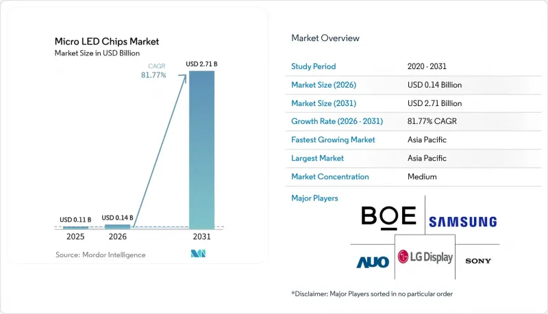
本報告按晶片尺寸(1-20毫米、20-50毫米及以上)、半導體材料(GaN/InGaN和AlGaInP)、應用領域(智慧型手錶和穿戴式設備、AR/VR近眼顯示器、電視、智慧型手機和平板電腦、車載顯示器、數位電子看板/大型顯示器等)以及地區(北美、歐洲、亞太地區等)進行細分。市場預測以美元計價。
全球MicroLED晶片市場趨勢與洞察
蘋果和三星加快了各自Micro LED技術的整合藍圖。
在2026年國際消費電子展(CES)上,三星的電視產品藍圖擴展至55-130吋的Micro RGB電視,並確認其產品將100%符合BT.2020色彩標準,但尚未獲得藍光安全認證。 LG則發表了Micro RGB Evo系列,顯示正在從OLED轉向垂直整合的供應鏈模式。SONY為其Crystal LED S系列註冊了「True RGB」商標,凸顯了對品牌建立的重視,認為這是高階品牌吸引早期用戶的手段。蘋果公司一直保持沉默,但其智慧手錶的原型機表明,蘋果採取了更探索性的方法,這與三星激進的規模策略形成了鮮明對比。這種分化正在造成一個兩極化的生態系統,電視收入抵消了穿戴式裝置和AR設備晶片尺寸研發過程中累積的經驗。
透過擴大6吋GaN-on-Si晶圓的尺寸來降低成本
京東方華芯電子投資7億美元的珠海計畫預計每年可生產5.8萬片6吋晶圓,其有效晶片面積將是傳統4吋生產線的四倍,單晶片外延成本降低約50%。根據PlayNitride預測,這項技術進步將使微型LED晶片市場在2028年達到與OLED市場同等的規模,尤其是在高亮度應用領域。湖南大學研發的亮度超過1000萬尼特的6吋GaN-on-Si晶圓證明,即使在更大直徑下也能確保光學完整性。根據《晶片技術創新法案》(CHIPS Act),GlobalFoundries獲得了15億美元的津貼,用於在西半球建立GaN-on-Si供應鏈,從而降低汽車和國防應用領域的地緣政治風險。這些進展共同縮小了微型LED與OLED的成本差距,並加速了供應鏈的地域轉移。
使用小於 4 英吋的晶圓製造小於 10µm 的紅色 LED,其良率低於 60%。
採用氮化鋁鈍化後,尺寸小於10µm的AlGaInP紅色晶片的外部量子效率已提升至22.3%,但商業性良率仍遠低於綠色和藍色晶片。側壁氧化可降低非輻射複合,但尚無法將良率提升至60%以上,導致廢料處理成本增加,進而擠壓利潤空間。三星和LG正透過在電視面板中使用尺寸更大的紅色晶片來應對這項挑戰,從而減少每個面板上的晶片數量。同時,採用量子點降壓轉換器的藍色GaN陣列正被應用於穿戴式裝置和AR設備,這增加了成本並提高了製造流程的難度。業界普遍認為,使用6吋AlGaInP晶圓可以降低邊緣抑制和溫度梯度,但目前尚無該尺寸晶圓的官方良率數據。
細分市場分析
預計1-20µm尺寸段的複合年成長率將達到83.21%,在所有尺寸等級中增速最高。這是因為Garmin售價1999.99美元的Fenix 8 Pro MicroLED顯示器證明,消費者願意為4500尼特的戶外可視亮度買單。 Jade Bird Display的10160 PPI Roadrunner微型面板則表明,像素密度而非晶圓成本將成為近視顯示器普及的關鍵因素。然而,其電池續航力仍落後於AMOLED,需要進一步整合驅動IC來彌補這一差距。
大型顯示器正朝著 50-100µm 晶片尺寸發展,這種尺寸的晶片良率更高,且對大規模晶片轉移的容差要求更低。三星的 130 吋型號和 LG 的 100 吋型號均採用小於 100µm 的 RGB LED,在實現 100% BT.2020 色域覆蓋的同時,還能有效控制成本,即使螢幕大小尺寸巨大,堪比牆面大小。汽車抬頭顯示器 (HUD) 則處於中間位置,並採用 20-50µm 晶片尺寸,以平衡密度和吞吐量。京東方 (BOE) 的 HERO 2.0 和天馬 (Tianma) 的模組正是這種最佳平衡的體現。
區域分析
亞太地區是microLED晶片市場的核心,預計到2025年將佔全球收入的62.30%,複合年成長率高達84.36%。京東方珠海工廠年產5.8萬片晶圓,三安光電擴建5000萬片Mini-LED生產線,充分體現了中國「速度與規模」的模式,為該地區提供了無與倫比的晶片供應深度。台灣在超高解析度細分市場佔據領先地位。友達光電獲得Garmin面板訂單,日月光在高雄投資5.79億美元建造後端工廠,都體現了其生態系統戰略。韓國在整合電視組裝領先,但仍大量依賴進口晶片,顯示其上游工程仍有投資空間。
北美市場的前景取決於《晶片法案》(CHIPS Act)的實施。全球晶圓代工廠正投資15億美元用於氮化鎵矽基(GaN-on-Si)生產線,而英特爾和台積電則合計籌集255億美元用於建造先進節點晶圓廠,這些晶圓廠能夠生產微型LED和驅動元件。自2026年1月起,對進口先進晶片徵收25%的關稅可能會促使原始設備製造商(OEM)轉向國內採購,但這將導致短期成本上升。歐洲缺乏類似的獎勵,其外延和麵板產品依賴進口,不過標緻等汽車OEM廠商的興趣表明,歐洲市場存在潛在需求。
南美洲和中東是早期市場,高階戶外標誌和汽車升級改造有望成為推動微型LED普及的催化劑。雖然目前尚未實現在地化生產,但微型LED的長壽命和高亮度使其在旗艦店外觀和豪華電動車儀錶板等領域具有應用潛力。監管方面的不足,尤其是在汽車安全標準方面,仍然是全球面臨的挑戰,即使技術成熟,也會延緩其普及。
其他好處:
- Excel格式的市場預測(ME)表
- 3個月的分析師支持
目錄
第1章:引言
- 研究假設和市場定義
- 調查範圍
第2章:調查方法
第3章執行摘要
第4章 市場狀況
- 市場概覽
- 市場促進因素
- 蘋果和三星加快了各自Micro LED技術的整合藍圖。
- 透過擴大6吋GaN-on-Si晶圓的尺寸來降低成本
- 雷射傳質吞吐量顯著提升:超過 400 個晶片/秒
- 汽車製造商要求電動車平台配備即使在陽光下也清晰可見的抬頭顯示器。
- 政府對採用CHIPS方法的國內微顯示器製造廠獎勵
- 量子點可實現超過 80% 的顏色轉換效率。
- 市場限制因素
- 使用小於 4 英吋晶圓的紅色 LED(尺寸小於 10µm)的市佔率(良率低於 60%)。
- 6億美元的資金障礙阻礙了新建大型管道的資本投資。
- 微型LED抬頭顯示器缺乏汽車產業認證標準
- 東亞地區氮化鎵矽基晶片供應集中
- 產業供應鏈分析
- 宏觀經濟因素對市場的影響
- 監理情勢
- 技術展望
- 波特五力分析
第5章 市場規模與成長預測
- 按尖端尺寸
- 1~20µm
- 20~50µm
- 50~100µm
- 透過半導體材料
- GaN/InGaN
- AlGaInP
- 透過使用
- 智慧型手錶和穿戴式裝置
- AR/VR近眼顯示器
- 電視機
- 智慧型手機和平板電腦
- 汽車顯示器
- 數位電子看板/大型顯示螢幕
- 其他用途(工業、醫療)
- 按地區
- 北美洲
- 歐洲
- 亞太地區
- 南美洲
- 中東和非洲
第6章 競爭情勢
- 市場集中度
- 策略趨勢
- 市佔率分析
- 公司簡介
- Samsung Electronics Co., Ltd.
- LG Display Co., Ltd.
- Sony Group Corporation
- AUO Corporation
- PlayNitride Inc.
- Epistar Corporation
- Jade Bird Display Inc.
- Plessey Semiconductors Ltd.
- Aledia SA
- VueReal Inc.
- San'an Optoelectronics Co., Ltd.
- Innolux Corporation
- Leyard Optoelectronic Co., Ltd.
- Unilumin Group Co., Ltd.
- Kyocera Corporation
- Cree LED, a Smart Global Holdings Company
- OSRAM Opto Semiconductors GmbH
第7章 市場機會與未來展望
According to Mordor Intelligence, the micro LED chips market size is projected to expand from USD 0.108 billion in 2025 and USD 0.137 billion in 2026 to USD 2.71 billion by 2031, registering a CAGR of 81.77% between 2026 and 2031.
This report is Segmented by Chip Size (1-20 Mm, 20-50 Mm, and More), Semiconductor Material (GaN/InGaN and AlGaInP), Application (Smartwatches and Wearables, AR/VR Near-Eye Displays, Television, Smartphones and Tablets, Automotive Displays, Digital Signage/Large Displays, and More), and Geography (North America, Europe, Asia Pacific, and More). The Market Forecasts are Provided in Terms of Value (USD).
Global Micro LED Chips Market Trends and Insights
Accelerating Apple and Samsung In-house Micro LED Integration Roadmaps
CES 2026 confirmed that Samsung's television roadmap now spans 55-130-inch Micro RGB models, achieving 100% BT.2020 color without blue-light hazard certification. LG countered with its Micro RGB Evo series, signaling a strategic pivot away from reliance on OLEDs and toward vertically integrated supply chains. Sony trademarked "True RGB" for its Crystal LED S Series, underscoring that premium brands see branding as a lever to capture early adopters. Apple remains publicly silent, but its watch prototypes suggest an exploratory posture that contrasts with Samsung's aggressive scale-up. This divergence creates a two-speed ecosystem where television economics may subsidize die-size learning curves for wearable and AR form factors.
Cost Declines from Six-Inch GaN-on-Si Wafer Scale-Up
BOE HC Semitek's USD 700 million Zhuhai project will deliver 58,000 six-inch wafers annually, quadrupling usable die area relative to legacy four-inch lines and slashing per-chip epitaxial cost by roughly 50%. PlayNitride projects that the learning curve will push the micro LED chip market to market size parity with OLED by 2028 for high-brightness use cases. Hunan University's six-inch GaN-on-Si wafers exceeding 10 million nits confirm optical integrity at larger diameters. A USD 1.5 billion CHIPS Act award is enabling GlobalFoundries to build a Western Hemisphere GaN-on-Si source, reducing geopolitical risk for automotive and defense applications. Together, these moves compress the cost gap with OLED and reposition supply chains geographically.
Yield < 60% for Sub-10 µm Red LEDs Below 4-Inch Wafers
The external quantum efficiency of sub-10 µm AlGaInP red dies rose to 22.3% with aluminum-nitride passivation, yet commercial yields still trail those of green and blue counterparts by a wide margin. Side-wall oxidation reduces non-radiative recombination but has not lifted yields above 60%, creating scrap costs that erode margins. Samsung and LG navigate this by using larger red dies for televisions, where die counts per panel are lower. Wearable and AR devices instead deploy blue GaN arrays with quantum-dot down-conversion, adding cost and process steps. Industry consensus holds that six-inch AlGaInP wafers could reduce edge exclusion and thermal gradients, but no public yield data yet exist for that diameter.
Other drivers and restraints analyzed in the detailed report include:
- Laser-Based Mass-Transfer Throughput Gains > 400 Chips/Sec
- Automotive OEM Demand for Sun-Readable HUDs in EV Platforms
- > USD 600 M CapEx Barrier for Greenfield High-Volume Lines
For complete list of drivers and restraints, kindly check the Table Of Contents.
Segment Analysis
The 1-20 µm segment is forecast to post an 83.21% CAGR, the fastest among all size classes, as Garmin's USD 1,999.99 Fenix 8 Pro MicroLED proves consumer readiness to pay for 4,500-nit daylight performance. Jade Bird Display's 10,160 PPI Roadrunner micro panel showcases that density, not die cost, defines near-eye adoption curves. However, battery life still trails AMOLED, and driver IC integration must improve to close the power gap.
Large-format displays gravitate toward 50-100 µm dies, where yields are higher, and mass-transfer tolerances are looser. Samsung's 130-inch set and LG's 100-inch model rely on sub-100 µm RGB LEDs to hit 100% BT.2020 color while maintaining cost discipline at wall-scale diagonals. Automotive HUD units sit between, using 20-50 µm dies to balance density with throughput; BOE's HERO 2.0 and Tianma's modules exemplify this sweet spot.
Geography Analysis
Asia Pacific generated 62.30% of 2025 revenue and is projected to grow at an 84.36% CAGR, making it the anchor of the micro LED chips market. China's "speed-and-scale" model is epitomized by BOE's 58,000-wafer Zhuhai fab and San'an's 5,000 kk-unit mini-LED ramp, giving the region unmatched die supply depth. Taiwan champions ultra-high-resolution niches; AUO's Garmin panel win, and ASE's USD 579 million backend plant in Kaohsiung reflect an ecosystem strategy. South Korea leads in integrated TV assembly but still imports many chips, indicating room for upstream investment.
North America's outlook hinges on the execution of the CHIPS Act. USD 1.5 billion is funding GlobalFoundries' GaN-on-Si line, while Intel and TSMC are collecting a combined USD 25.5 billion for advanced-node fabs that may house micro LED and driver components. A 25% tariff on imported advanced chips, effective January 2026, could nudge OEMs toward domestic sourcing but raises near-term costs. Europe lacks comparable incentives, relying on imports for epitaxy and panels, though automotive OEM interest via Peugeot indicates latent demand.
South America and the Middle East are early-stage markets where premium outdoor signage and automotive upgrades will seed adoption. Local manufacturing is absent, but micro LEDs' longevity and brightness can justify imports for flagship retail facades and luxury EV dashboards. Regulatory gaps, especially around automotive safety standards, are global, slowing deployment even where technical readiness is proven.
- Samsung Electronics Co., Ltd.
- LG Display Co., Ltd.
- Sony Group Corporation
- AUO Corporation
- PlayNitride Inc.
- Epistar Corporation
- Jade Bird Display Inc.
- Plessey Semiconductors Ltd.
- Aledia S.A.
- VueReal Inc.
- San'an Optoelectronics Co., Ltd.
- Innolux Corporation
- Leyard Optoelectronic Co., Ltd.
- Unilumin Group Co., Ltd.
- Kyocera Corporation
- Cree LED, a Smart Global Holdings Company
- OSRAM Opto Semiconductors GmbH
Additional Benefits:
- The market estimate (ME) sheet in Excel format
- 3 months of analyst support
TABLE OF CONTENTS
1 INTRODUCTION
- 1.1 Study Assumptions and Market Definition
- 1.2 Scope of the Study
2 RESEARCH METHODOLOGY
3 EXECUTIVE SUMMARY
4 MARKET LANDSCAPE
- 4.1 Market Overview
- 4.2 Market Drivers
- 4.2.1 Accelerating Apple and Samsung In-house Micro LED Integration Roadmaps
- 4.2.2 Cost Declines from Six-Inch GaN-on-Si Wafer Scale-Up
- 4.2.3 Laser-Based Mass-Transfer Throughput Gains >400 Chips/Sec
- 4.2.4 Automotive OEM Demand for Sun-Readable HUDs in EV Platforms
- 4.2.5 Government CHIPS-style Incentives for Domestic Micro-Display Fabs
- 4.2.6 Quantum-Dot Color Conversion Surpassing 80 % Efficiency
- 4.3 Market Restraints
- 4.3.1 Yield <60 % for Sub-10 µm Red LEDs Below 4-inch Wafers
- 4.3.2 >USD 600 M CapEx Barrier for Greenfield High-Volume Lines
- 4.3.3 Lack of Automotive Qualification Standards for Micro LED HUDs
- 4.3.4 Concentrated Supply of GaN-on-Si Wafers in East Asia
- 4.4 Industry Supply-Chain Analysis
- 4.5 Impact of Macroeconomic Factors on the Market
- 4.6 Regulatory Landscape
- 4.7 Technological Outlook
- 4.8 Porter's Five Forces Analysis
- 4.8.1 Threat of New Entrants
- 4.8.2 Bargaining Power of Suppliers
- 4.8.3 Bargaining Power of Buyers
- 4.8.4 Threat of Substitutes
- 4.8.5 Competitive Rivalry
5 MARKET SIZE AND GROWTH FORECASTS (VALUE)
- 5.1 By Chip Size
- 5.1.1 1-20 µm
- 5.1.2 20-50 µm
- 5.1.3 50-100 µm
- 5.2 By Semiconductor Material
- 5.2.1 GaN / InGaN
- 5.2.2 AlGaInP
- 5.3 By Application
- 5.3.1 Smartwatches & Wearables
- 5.3.2 AR/VR Near-Eye Displays
- 5.3.3 Television
- 5.3.4 Smartphones & Tablets
- 5.3.5 Automotive Displays
- 5.3.6 Digital Signage / Large Displays
- 5.3.7 Other Applications (Industrial, Medical)
- 5.4 By Geography
- 5.4.1 North America
- 5.4.2 Europe
- 5.4.3 Asia Pacific
- 5.4.4 South America
- 5.4.5 Middle East and Africa
6 COMPETITIVE LANDSCAPE
- 6.1 Market Concentration
- 6.2 Strategic Moves
- 6.3 Market Share Analysis
- 6.4 Company Profiles (includes Global Level Overview, Market Level Overview, Core Segments, Financials as available, Strategic Information, Market Rank/Share, Products and Services, Recent Developments)
- 6.4.1 Samsung Electronics Co., Ltd.
- 6.4.2 LG Display Co., Ltd.
- 6.4.3 Sony Group Corporation
- 6.4.4 AUO Corporation
- 6.4.5 PlayNitride Inc.
- 6.4.6 Epistar Corporation
- 6.4.7 Jade Bird Display Inc.
- 6.4.8 Plessey Semiconductors Ltd.
- 6.4.9 Aledia S.A.
- 6.4.10 VueReal Inc.
- 6.4.11 San'an Optoelectronics Co., Ltd.
- 6.4.12 Innolux Corporation
- 6.4.13 Leyard Optoelectronic Co., Ltd.
- 6.4.14 Unilumin Group Co., Ltd.
- 6.4.15 Kyocera Corporation
- 6.4.16 Cree LED, a Smart Global Holdings Company
- 6.4.17 OSRAM Opto Semiconductors GmbH
7 MARKET OPPORTUNITIES AND FUTURE OUTLOOK
- 7.1 White-Space and Unmet-Need Assessment

 MicroLED市場報告:趨勢、預測和競爭分析(至2035年)
 2026年全球微型發光二極體(LED)顯示器市場報告微型發光二極體(LED)晶片市場報告:趨勢、預測與競爭分析(至2035年)
 微型LED晶片及傳質材料市場機會、成長促進因素、產業趨勢分析及2026-2035年預測
 MicroLED:市場佔有率分析、行業趨勢和統計數據、成長預測(2026-2031)
 微型LED光學引擎市場:按組件、技術、材料、應用和終端用戶產業分類的全球預測(2026-2032年)微型LED晶圓質傳設備市場:2026-2032年全球預測(依設備類型、傳輸技術、晶圓尺寸、自動化程度及最終用途產業分類)
 MicroLED市場規模、佔有率和成長分析:按應用、顯示像素密度、最終用途和地區分類-產業預測(2026-2033年)
 MicroLED市場分析及預測(至2035年):按類型、產品、技術、組件、應用、材料類型、裝置、最終用戶和製程分類AR微光學引擎市場按技術、引擎類型、顯示類型、解析度和應用分類-2026-2032年全球預測