

 |
市場調查報告書
商品編碼
2109232
微型LED晶片及傳質材料市場機會、成長促進因素、產業趨勢分析及2026-2035年預測MicroLED Chip and Mass Transfer Materials Market Opportunity, Growth Drivers, Industry Trend Analysis, and Forecast 2026 - 2035 |
||||||

全球MicroLED晶片和質傳材料市場預計到2025年將達到1.6億美元,到2035年將以39.2%的複合年成長率成長,達到55億美元。
MicroLED晶片和大規模轉移材料市場構成了一個生態系統,專注於MicroLED晶片的製造以及先進材料的開發,這些材料能夠實現微型LED在顯示器背板上的高精度、大規模轉移。這些技術在下一代顯示器的製造中發揮著至關重要的作用,這些顯示器能夠提供更高的亮度、對比度、更高的能源效率和更長的使用壽命。隨著人們對高性能顯示技術的興趣日益濃厚,製造商紛紛將目光投向先進技術,以取代傳統的顯示技術,該市場正持續快速擴張。 MicroLED晶片憑藉其自發光特性、低功耗和高耐久性,在許多行業中獲得了越來越多的關注。對晶片製造技術的持續投入和轉移材料的創新正在增強產能並提高商業性可行性。同時,大規模轉移材料的進步使製造商能夠實現更高的貼片精度、更高的良率、更強的擴充性和更低的製造成本。這些發展為顯示器製造商創造了新的機遇,並推動MicroLED技術在各種顯示應用中的進一步商業化。
| 市場範圍 | |
|---|---|
| 開始年份 | 2025 |
| 預測期 | 2026-2035 |
| 初始市場規模 | 1.6億美元 |
| 預測金額 | 55億美元 |
| 複合年成長率 | 39.2% |
預計到2025年,MicroLED晶片市場規模將達到1.152億美元。消費者對更高亮度、更高能源效率和更出色視覺性能的需求不斷成長,持續推動MicroLED晶片在家用電子電器、汽車顯示系統和穿戴式科技領域的應用。製造商致力於在縮小晶片尺寸的同時提高像素密度,從而打造更緊湊、技術更先進的顯示器。晶片製造技術的不斷進步提升了顯示器的性能,並滿足了包括擴增實境(AR)和虛擬實境(VR)設備在內的先進視覺化技術不斷發展的需求。
預計到2025年,彈性體印章轉移(µTP)市場規模將達6,720萬美元。這種轉移方法使用軟性聚合物印章將MicroLED晶片精確地提升並定位到指定基板上,使其成為對精度要求極高的顯示器製造的理想選擇。雷射輔助轉移(LIFT/LLO)利用雷射能量分離並轉移MicroLED晶片,同時最大限度地減少物理接觸,從而提高定位精度並最大限度地減少製造過程中的機械應力。靜電轉移是一種利用可控靜電力高效移動和對準微型LED晶片的技術,為製造商提供了一種有效的方法來提高對準精度並最佳化整個製造過程中的轉移性能。
預計到2035年,北美MicroLED晶片和質傳材料市場規模將達12億美元。該地區持續受益於MicroLED研發舉措的不斷成長,這些投入正在加速推進先進顯示器製造、半導體創新和商業化進程。家用電子電器、汽車顯示器解決方案和穿戴式裝置對先進顯示技術的強勁需求,推動了市場的持續成長。美國透過在MicroLED晶片開發和傳質技術研究方面取得的持續進展,繼續為該地區的市場擴張做出重大貢獻。來自科技公司、顯示器開發商和半導體行業的持續支持,正在推動製造效率、整體顯示性能和產品品質的提升。
目錄
第1章:調查方法和範圍
第2章執行摘要
第3章 行業洞察
- 產業生態系分析
- 供應商情況
- 利潤率
- 每個階段增加的價值
- 影響價值鏈的因素
- 中斷
- 影響產業的因素
- 促進因素
- 對下一代顯示技術的需求日益成長
- 汽車顯示器的應用範圍不斷擴大
- 增加對顯示器製造創新領域的投資
- 產業潛在風險與挑戰
- 製造過程的高度複雜性
- 生產成本上升
- 市場機遇
- 新興的擴增實境(AR)和虛擬實境(VR)應用
- 軟性透明顯示器的開發
- 傳質材料和自動化技術的進步
- 促進因素
- 成長潛力分析
- 監理情勢
- 波特的分析
- PESTLE分析
- 技術與創新展望
- 最新科技趨勢
- 新興技術
- 價格趨勢
- 按地區
- 依組件類型
- 未來市場趨勢
- 專利趨勢
- 貿易統計
- 主要進口國
- 主要出口國
- 永續性和環境方面
- 永續計劃
- 減少廢棄物策略
- 生產中的能源效率
- 具有環保意識的舉措
- 考慮碳足跡
第4章 競爭情勢
- 介紹
- 企業市佔率分析
- 按地區
- 北美洲
- 歐洲
- 亞太地區
- 拉丁美洲
- 中東和非洲
- 按地區
- 企業矩陣分析
- 主要市場公司的競爭分析
- 競爭定位矩陣
- 主要進展
- 併購
- 夥伴關係和聯盟
- 新產品發布
- 業務拓展計劃
第5章 市場估計與預測:依組件類型分類,2022-2035年
- 微型LED晶片
- 單色晶片
- 全彩/單片RGB晶片
- 質傳材料
- 彈性體沖壓材料
- 雷射剝離(LLO)的犧牲層材料
- 臨時黏合劑
- 載體基板材料
- 流體和靜電組裝介質
第6章 市場估計與預測:依行動技術分類,2022-2035年
- 彈性體印章轉移(µTP)
- 雷射輔助運動(LIFT/LLO)
- 靜電運動
- 流體自組裝
- 混合轉移
第7章 市場估計與預測:依應用領域分類,2022-2035年
- 家用電子產品
- AR/VR 和微型顯示器
- 汽車顯示器
- 數位電子看板和商用顯示器
- 穿戴式裝置
- 其他
第8章 市場估計與預測:依地區分類,2022-2035年
- 北美洲
- 美國
- 加拿大
- 歐洲
- 德國
- 英國
- 法國
- 西班牙
- 義大利
- 其他歐洲國家
- 亞太地區
- 中國
- 印度
- 日本
- 澳洲
- 韓國
- 其他亞太國家
- 拉丁美洲
- 巴西
- 墨西哥
- 阿根廷
- 其他拉丁美洲國家
- 中東和非洲
- 沙烏地阿拉伯
- 南非
- UAE
- 其他中東和非洲國家
第9章:公司簡介
- Samsung Electronics
- ams OSRAM
- Jade Bird Display(JBD)
- Sanan Optoelectronics
- PlayNitride Display Co., Ltd.
- Lumileds Holding BV
- HC SemiTek Corp.(BOE HC SemiTek)
- ENNOSTAR Inc.
- Xiamen Changelight Co., Ltd.
- Aledia SA
- Porotech Ltd.
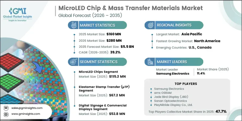
The Global MicroLED Chip & Mass Transfer Materials Market was valued at USD 160 million in 2025 and is estimated to grow at a CAGR of 39.2% to reach USD 5.5 billion by 2035.
The microLED chip & mass transfer materials market represents the ecosystem focused on manufacturing MicroLED chips and developing advanced materials that enable the large-scale transfer of microscopic LEDs onto display backplanes with high precision. These technologies play a critical role in producing next-generation displays that deliver superior brightness, enhanced contrast, improved energy efficiency, and extended operational life. Growing interest in high-performance display technologies continues to accelerate market expansion as manufacturers shift their focus toward advanced alternatives to conventional display technologies. MicroLED chips provide self-emissive performance while supporting lower power consumption and greater durability, making them increasingly attractive across multiple industries. Continuous investments in chip manufacturing technologies and transfer material innovation are strengthening production capabilities and improving commercial viability. At the same time, advancements in mass-transfer materials are helping manufacturers achieve higher placement accuracy, better production yields, greater scalability, and lower manufacturing costs. These developments are creating new opportunities for display manufacturers while supporting broader commercialization of MicroLED technology across a wide range of display applications.
| Market Scope | |
|---|---|
| Start Year | 2025 |
| Forecast Year | 2026-2035 |
| Start Value | $160 Million |
| Forecast Value | $5.5 Billion |
| CAGR | 39.2% |
The microLED chips segment accounted for USD 115.2 million in 2025. Rising demand for brighter displays, greater energy efficiency, and enhanced visual performance continues to accelerate the adoption of MicroLED chips across consumer electronics, automotive display systems, and wearable technology. Manufacturers are placing greater emphasis on reducing chip size while increasing pixel density, allowing displays to become more compact and technologically advanced. Ongoing improvements in chip fabrication technologies are enhancing display performance and supporting the evolving requirements of advanced visualization, including augmented and virtual reality devices.
The elastomer stamp transfer (µTP) segment generated USD 67.2 million in 2025. This transfer method uses flexible polymer stamps to accurately lift and position MicroLED chips onto the intended substrate, making it highly suitable for precision-focused display manufacturing. Laser-Assisted Transfer (LIFT/LLO) utilizes laser energy to release and transfer MicroLED chips with limited physical contact, improving placement precision while minimizing mechanical stress during manufacturing. Electrostatic Transfer applies controlled electrostatic forces to move and align microscopic LED chips efficiently, providing manufacturers with an effective approach to enhance alignment accuracy and optimize transfer performance throughout the production process.
North America MicroLed Chip & Mass Transfer Materials Market is anticipated to reach USD 1.2 billion by 2035. The region continues to benefit from increasing investments in advanced display manufacturing, semiconductor innovation, and MicroLED research initiatives that are accelerating commercialization efforts. Strong demand for advanced display technologies across consumer electronics, automotive display solutions, and wearable devices is contributing to sustained market growth. The United States remains a major contributor to regional expansion through continued advancements in MicroLED chip development and transfer technology research. Ongoing support from technology companies, display developers, and the semiconductor industry is helping improve manufacturing efficiency while enhancing overall display performance and production quality.
Major companies operating in the global microLED chip & mass transfer materials market include Samsung Electronics, ams OSRAM, Jade Bird Display (JBD), Sanan Optoelectronics, PlayNitride Display Co., Ltd., Lumileds Holding B.V., HC SemiTek Corp. (BOE HC SemiTek), ENNOSTAR Inc., Xiamen Changelight Co., Ltd., Aledia S.A., and Porotech Ltd. Companies operating in the microLED chip & mass transfer materials market are strengthening their market position by investing heavily in research and development to improve chip efficiency, transfer precision, and manufacturing scalability. Many participants are expanding production capabilities to support future commercial demand while optimizing fabrication processes to enhance product quality and reduce production costs. Strategic collaborations with display manufacturers, semiconductor companies, and technology partners are helping accelerate innovation and product commercialization. Businesses are also introducing advanced manufacturing technologies to improve production yields and increase operational efficiency.
Table of Contents
Chapter 1 Methodology & Scope
- 1.1 Market scope and definition
- 1.2 Research design
- 1.2.1 Research approach
- 1.2.2 Data collection methods
- 1.3 Data mining sources
- 1.3.1 Global
- 1.3.2 Regional/Country
- 1.4 Base estimates and calculations
- 1.4.1 Base year calculation
- 1.4.2 Key trends for market estimation
- 1.5 Primary research and validation
- 1.5.1 Primary sources
- 1.6 Forecast model
- 1.7 Research assumptions and limitations
Chapter 2 Executive Summary
- 2.1 Industry 360° synopsis
- 2.2 Key market trends
- 2.2.1 Component Type
- 2.2.2 Transfer Technology
- 2.2.3 Application
- 2.2.4 Regional
- 2.3 TAM Analysis, 2026-2035
- 2.4 CXO perspectives: Strategic imperatives
- 2.5 Future outlook and strategic recommendations
Chapter 3 Industry Insights
- 3.1 Industry ecosystem analysis
- 3.1.1 Supplier landscape
- 3.1.2 Profit margin
- 3.1.3 Value addition at each stage
- 3.1.4 Factor affecting the value chain
- 3.1.5 Disruptions
- 3.2 Industry impact forces
- 3.2.1 Growth drivers
- 3.2.1.1 Rising demand for next-generation display technologies
- 3.2.1.2 Expansion of automotive display applications
- 3.2.1.3 Growing investments in display manufacturing innovation
- 3.2.2 Industry pitfalls and challenges
- 3.2.2.1 High manufacturing complexity
- 3.2.2.2 Elevated production costs
- 3.2.3 Market opportunities
- 3.2.3.1 Emerging augmented reality and virtual reality applications
- 3.2.3.2 Development of flexible and transparent displays
- 3.2.3.3 Advancements in mass transfer materials and automation technologies
- 3.2.1 Growth drivers
- 3.3 Growth potential analysis
- 3.4 Regulatory landscape
- 3.4.1 North America
- 3.4.2 Europe
- 3.4.3 Asia Pacific
- 3.4.4 Latin America
- 3.4.5 Middle East & Africa
- 3.5 Porter’s analysis
- 3.6 PESTEL analysis
- 3.7 Technology and innovation landscape
- 3.7.1 Current technological trends
- 3.7.2 Emerging technologies
- 3.8 Price trends
- 3.8.1 By region
- 3.8.2 By component type
- 3.9 Future market trends
- 3.10 Patent landscape
- 3.11 Trade statistics (HS code)
- 3.11.1 Major importing countries
- 3.11.2 Major exporting countries
- 3.12 Sustainability and environmental aspects
- 3.12.1 Sustainable practices
- 3.12.2 Waste reduction strategies
- 3.12.3 Energy efficiency in production
- 3.12.4 Eco-friendly initiatives
- 3.13 Carbon footprint consideration
Chapter 4 Competitive Landscape, 2025
- 4.1 Introduction
- 4.2 Company market share analysis
- 4.2.1 By region
- 4.2.1.1 North America
- 4.2.1.2 Europe
- 4.2.1.3 Asia Pacific
- 4.2.1.4 LATAM
- 4.2.1.5 MEA
- 4.2.1 By region
- 4.3 Company matrix analysis
- 4.4 Competitive analysis of major market players
- 4.5 Competitive positioning matrix
- 4.6 Key developments
- 4.6.1 Mergers & acquisitions
- 4.6.2 Partnerships & collaborations
- 4.6.3 New product launches
- 4.6.4 Expansion plans
Chapter 5 Market Estimates and Forecast, By Component Type, 2022–2035 (USD Million) (Kilo Tons)
- 5.1 Key trends
- 5.2 MicroLED Chips
- 5.2.1 Monochromatic Chips
- 5.2.2 Full-Color/Monolithic RGB Chips
- 5.3 Mass Transfer Materials
- 5.3.1 Elastomer Stamp Materials
- 5.3.2 Laser Lift-Off (LLO) Sacrificial Layer Materials
- 5.3.3 Temporary Bonding Adhesives
- 5.3.4 Carrier Substrate Materials
- 5.3.5 Fluidic & Electrostatic Assembly Media
Chapter 6 Market Estimates and Forecast, By Transfer technology, 2022–2035 (USD Million) (Kilo Tons)
- 6.1 Key trends
- 6.2 Elastomer Stamp Transfer (µTP)
- 6.3 Laser-Assisted Transfer (LIFT/LLO)
- 6.4 Electrostatic Transfer
- 6.5 Fluidic Self-Assembly
- 6.6 Hybrid Transfer
Chapter 7 Market Estimates and Forecast, By Application, 2022–2035 (USD Million) (Kilo Tons)
- 7.1 Key trends
- 7.2 Consumer Electronics
- 7.3 AR/VR & Microdisplays
- 7.4 Automotive Displays
- 7.5 Digital Signage & Commercial Displays
- 7.6 Wearable Devices
- 7.7 Others
Chapter 8 Market Estimates and Forecast, By Region, 2022–2035 (USD Million) (Kilo Tons)
- 8.1 Key trends
- 8.2 North America
- 8.2.1 U.S.
- 8.2.2 Canada
- 8.3 Europe
- 8.3.1 Germany
- 8.3.2 UK
- 8.3.3 France
- 8.3.4 Spain
- 8.3.5 Italy
- 8.3.6 Rest of Europe
- 8.4 Asia Pacific
- 8.4.1 China
- 8.4.2 India
- 8.4.3 Japan
- 8.4.4 Australia
- 8.4.5 South Korea
- 8.4.6 Rest of Asia Pacific
- 8.5 Latin America
- 8.5.1 Brazil
- 8.5.2 Mexico
- 8.5.3 Argentina
- 8.5.4 Rest of Latin America
- 8.6 Middle East and Africa
- 8.6.1 Saudi Arabia
- 8.6.2 South Africa
- 8.6.3 UAE
- 8.6.4 Rest of Middle East and Africa
Chapter 9 Company Profiles
- 9.1 Samsung Electronics
- 9.2 ams OSRAM
- 9.3 Jade Bird Display (JBD)
- 9.4 Sanan Optoelectronics
- 9.5 PlayNitride Display Co., Ltd.
- 9.6 Lumileds Holding B.V.
- 9.7 HC SemiTek Corp. (BOE HC SemiTek)
- 9.8 ENNOSTAR Inc.
- 9.9 Xiamen Changelight Co., Ltd.
- 9.10 Aledia S.A.
- 9.11 Porotech Ltd.

 MicroLED市場報告:趨勢、預測和競爭分析(至2035年)
 2026年全球微型發光二極體(LED)顯示器市場報告微型發光二極體(LED)晶片市場報告:趨勢、預測與競爭分析(至2035年)
 MicroLED:市場佔有率分析、行業趨勢和統計數據、成長預測(2026-2031)MicroLED晶片:市佔率分析、產業趨勢與統計、成長預測(2026-2031年)
 微型LED光學引擎市場:按組件、技術、材料、應用和終端用戶產業分類的全球預測(2026-2032年)微型LED晶圓質傳設備市場:2026-2032年全球預測(依設備類型、傳輸技術、晶圓尺寸、自動化程度及最終用途產業分類)
 MicroLED市場規模、佔有率和成長分析:按應用、顯示像素密度、最終用途和地區分類-產業預測(2026-2033年)
 MicroLED市場分析及預測(至2035年):按類型、產品、技術、組件、應用、材料類型、裝置、最終用戶和製程分類AR微光學引擎市場按技術、引擎類型、顯示類型、解析度和應用分類-2026-2032年全球預測