


 |
市場調查報告書
商品編碼
2044007
優質拋光晶圓:市場佔有率分析、行業趨勢和統計數據、成長預測(2026-2031 年)Prime Polished Wafer - Market Share Analysis, Industry Trends & Statistics, Growth Forecasts (2026 - 2031) |
||||||

※ 本網頁內容可能與最新版本有所差異。詳細情況請與我們聯繫。
預計到 2025 年,優質拋光晶圓市場將達到 88.6 億平方英寸,到 2026 年將達到 92.6 億平方英寸,到 2031 年將達到 117.6 億平方英寸,2026 年至 2031 年的複合年成長率為 4.88%。
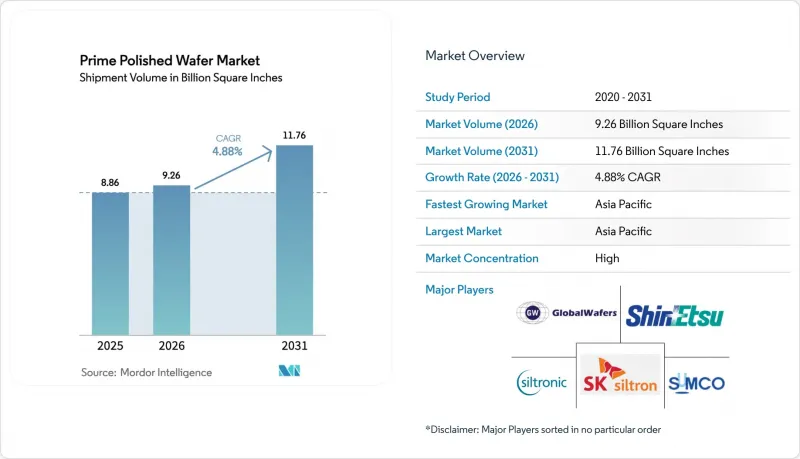
半導體製造商正將資金重新分配到先進邏輯節點、汽車電氣化和高頻寬記憶體領域,這些領域對晶圓表面積的消耗速度遠超傳統家用電子電器產品的週期。代工廠向3奈米以下製程技術的轉型,以及穿透矽通孔(TSV)封裝技術的擴展,正在推動對300毫米直徑晶圓的需求,而該尺寸的晶圓已在優質拋光晶圓市場佔據主導地位。亞太地區憑藉契約製造基地保持主導地位,但美國和歐洲正利用補償將獎勵產能遷回國內,即使這意味著成本增加。供應商對投資新的晶體生長設備仍然持謹慎態度,因為一條300毫米高純度晶錠生產線的成本可能在200萬美元到500萬美元之間,而且認證可能需要長達兩年的時間。
全球優質拋光晶圓市場趨勢與洞察
電動車的廣泛普及以及向800V車輛平台的過渡
採用 800V 架構的電動車需要碳化矽 (SiC) 牽引逆變器,其單位裝置所需的優質拋光晶圓數量遠高於矽元件。雖然 Wolfspeed 計劃於 2025 年 9 月開始商業化生產 200mm SiC,屆時每片晶圓的晶片數量將增加約 85%,但 7-14 天的晶體生長週期仍然是供應瓶頸。多家大型汽車製造商已對電壓高達 1200V 的 SiC MOSFET 進行認證,進一步推高了市場需求。
800V充電基礎設施快速發展
在歐洲和中國,數千座功率在150至350千瓦之間的充電站正在安裝,這些充電站採用碳化矽(SiC)模組進行整流和功率因數校正。每個超快充電樁需要多片200毫米的矽晶圓,這催生了對優質拋光矽晶圓市場的二次需求。政府補貼正在加快安裝進度,迫使供應商提高其整體產能。
200mm基板供不應求
200毫米碳化矽晶錠需要較長的生長週期和專用爐。由於汽車OEM廠商簽訂多年契約,小規模客戶的基板前置作業時間可能超過40週,導致其他高階拋光晶圓市場的參與者爭相搶佔配額。
細分市場分析
截至2025年,300毫米晶圓將佔據優質拋光晶圓市場73.39%的佔有率,預計到2031年將以5.55%的複合年成長率成長。台積電計畫在2026年投入560億美元資本支出,其中70-80%將用於3奈米及以下過程的邏輯半導體,凸顯了向更大直徑過程的持續轉型。隨著高頻寬記憶體和人工智慧加速器對每台伺服器晶圓面積的需求是傳統工作負載的4-8倍,這種直徑優質拋光晶圓的市場規模將持續擴大。英特爾在亞利桑那州投資1,650億美元的「超級晶圓廠」(Gigafab)叢集和位於德克薩斯州的全球晶圓生產線將創建新的物流樞紐,同時提高區域冗餘度並滿足國內採購法規。
200mm規格的晶圓對於模擬、混合訊號和功率裝置,尤其是SiC MOSFET而言仍然至關重要,因為較小的直徑仍然具有經濟優勢。 Okmetic在芬蘭的擴張以及Wolfspeed的200mm SiC晶圓表明,供應商正在採用雙軌策略,以滿足主流矽晶片和特殊需求。雖然小於150mm的晶圓規格正在減少,但它們仍然用於傳統的汽車微控制器和射頻GaAs裝置。隨著晶體生長技術的進步和缺陷密度的降低,200mm SiC的供應在2028年後可能會有所緩解,但就目前而言,供不應求仍然存在,導致價格居高不下,並加劇了晶圓廠之間為確保與多家供應商合作而進行的競爭。
《優質拋光晶圓市場報告》以晶圓直徑(150毫米及以下、200毫米、300毫米)、半導體裝置類型(邏輯元件、記憶體、模擬器零件、分立裝置及其他)、最終用戶(家用電子電器、工業、通訊、汽車及其他)和地區(北美、歐洲、亞太、南美、中東和非洲)進行細分。市場預測以體積(平方英吋)為單位。
區域分析
預計到2025年,亞太地區將佔全球優質拋光晶圓出貨量的81.39%,並在2031年之前以5.21%的複合年成長率成長。台積電、三星和SK Siltron等區域領導企業正持續擴展其高度整合的叢集涵蓋前端、封裝和測試等環節。中國中芯國際正計劃在2026年將其晶圓產能提升至每月4萬片(12吋當量),儘管面臨設備出口限制,運轉率仍高達95.7%。中國475億美元的積體電路基金三期計畫提供的補貼正在支持國內碳化矽供應鏈的發展。
在北美,一項獎勵390億美元的《晶片製造和生產法案》(CHIPS Act)正被用於扭轉數十年來境外外包的局面。 GlobalWafers公司投資35億美元在德克薩斯建設的工廠、英特爾位於亞利桑那州的超級晶圓廠以及Wolfspeed公司的碳化矽巨型工廠,都推動了全部區域對優質拋光晶圓需求的激增。此外,墨西哥在組裝和測試領域日益重要的地位也進一步刺激了下游工藝的需求。
儘管歐洲在尖端邏輯晶片領域仍面臨晶圓廠短缺的問題,但在戰略材料領域卻展現出強勁的實力。義法半導體已獲得29億歐元(約32億美元)的投資,用於擴大其在義大利的碳化矽業務,並正就台積電在德勒斯登營運的工廠進行持續磋商。如果該專案得以實現,將使300毫米汽車半導體的產能本地化。 Soitec和Siltronic等公司提供在地化的SOI和高平整度基板,使歐洲能夠在優質拋光晶圓市場價值鏈中保持關鍵地位。南美洲、中東和非洲的新投資往往優先考慮服務更貼近終端市場的汽車和工業客戶的成熟節點晶圓廠。
其他好處:
- Excel格式的市場預測(ME)表
- 3個月的分析師支持
目錄
第1章:引言
- 研究假設和市場定義
- 調查範圍
第2章:調查方法
第3章執行摘要
第4章 市場狀況
- 市場概覽
- 產業價值鏈分析
- 監理情勢
- 宏觀經濟因素的影響
- 技術分析
- 監理展望
- 波特五力分析
- 供應商的議價能力
- 買方的議價能力
- 新進入者的威脅
- 替代品的威脅
- 競爭公司之間的競爭
- 市場促進因素
- 電動車的廣泛普及以及向800V車輛平台的過渡
- 800V充電基礎設施快速發展
- 在高溫和高頻性能方面優於矽
- 政府對寬能隙裝置製造的支援措施
- 中國垂直整合型碳化矽供應鏈的崛起
- 200mm 塊體生長技術新突破,降低缺陷密度
- 市場限制因素
- 200mm基板供不應求
- 包裝引起的熱機械應力
- 資本密集型晶體生長裝置
- 碳化矽切削屑回收利用面臨的挑戰
第5章 市場規模與成長預測
- 依晶圓直徑
- 最大可達 150 毫米
- 200 mm
- 300 mm
- 以半導體裝置類型分類
- 邏輯
- 記憶
- 模擬
- 離散的
- 其他類型的半導體裝置(光電子元件、感測器、微型元件)
- 最終用戶
- 家用電子產品
- 手機和智慧型手機
- 個人電腦和伺服器
- 工業的
- 溝通
- 車
- 其他終端用戶應用程式
- 家用電子產品
- 按地區
- 北美洲
- 美國
- 加拿大
- 墨西哥
- 歐洲
- 德國
- 英國
- 法國
- 其他歐洲地區
- 亞太地區
- 中國
- 日本
- 印度
- 韓國
- 台灣
- 亞太其他地區
- 南美洲
- 中東
- 非洲
- 北美洲
第6章 競爭情勢
- 市場集中度
- 策略趨勢
- 市佔率分析
- 公司簡介
- Shin-Etsu Handotai Co., Ltd.
- SUMCO Corporation
- GlobalWafers Co., Ltd.
- Siltronic AG
- SK Siltron Co., Ltd.
- Soitec SA
- Okmetic Oyj
- Wafer Works Corporation
- Ferrotec Holdings Corporation
- Hangzhou Crystal Silicon Technology Co., Ltd.
- Poshing Electronics Co., Ltd.
- MiCo Co., Ltd.
- Tokuyama Corporation
- Topsil Semiconductor Materials A/S
- GCL Technology Holdings Limited
- Zhejiang Jingsheng Mechanical & Electrical Co., Ltd.
- II-VI Incorporated
- AEPI Group(Sil'Tronix Silicon Technologies)
- Advantest Corporation
- Shanghai SIM-AXIS Semiconductor Materials Co., Ltd.
第7章 市場機會與未來展望
The prime polished wafer market size is projected to be 8.86 billion square inches in 2025, 9.26 billion square inches in 2026, and reach 11.76 billion square inches by 2031, growing at a CAGR of 4.88% from 2026 to 2031.
Semiconductor manufacturers are reallocating capital toward advanced logic nodes, automotive electrification, and high-bandwidth memory, all of which consume wafer surface area far more rapidly than traditional consumer-electronics refresh cycles. Foundries' shift to sub-3 nm process technology, coupled with the ramp-up of through-silicon-via packaging, is concentrating demand in the 300 mm diameter class that already dominates the prime polished wafer market. Asia-Pacific's contract manufacturing base keeps the region in a leadership position, while the United States and Europe are using incentive packages to on-shore strategic capacity despite the resulting cost penalties. Suppliers remain cautious on new crystal-growth investments because each 300 mm high-purity ingot line ranges from USD 2 million to USD 5 million and can take two years to qualify.
Global Prime Polished Wafer Market Trends and Insights
Rising EV Penetration and Shift Toward 800-V Vehicle Platforms
Electric vehicles adopting 800-volt architectures require silicon-carbide traction inverters that consume far larger prime polished wafer volumes per car than silicon devices. Wolfspeed's commercial 200 mm SiC launch in September 2025 increases chips-per-wafer by roughly 85%, yet supply is still bottlenecked by 7- to 14-day crystal-growth cycles. Multiple major automakers already qualify SiC MOSFETs rated up to 1,200 V, pushing demand firmly upward.
Rapid Build-Out of 800-V Charging Infrastructure
Europe and China are adding thousands of 150- to 350-kW charging stalls that embed SiC modules for rectification and power-factor correction. Each ultra-fast charger needs multiple 200 mm wafers, creating a second-order pull on the prime polished wafer market. Subsidies accelerate installation schedules, compressing suppliers' ability to add new boule capacity.
Limited Availability of 200 mm Substrates
200 mm SiC boules require long growth times and specialized furnaces. Substrate lead times stretch beyond 40 weeks for smaller customers as automotive OEMs lock in multi-year contracts, leaving the rest of the prime polished wafer market scrambling for allocation.
Other drivers and restraints analyzed in the detailed report include:
- High-Temperature, High-Frequency Performance Advantages Over Si
- Government Incentives for Wide-Band-Gap Fabs
- Packaging-Induced Thermo-Mechanical Stress
For complete list of drivers and restraints, kindly check the Table Of Contents.
Segment Analysis
The 300 mm class accounted for 73.39% of prime polished wafer market share in 2025 and is forecast to grow at a 5.55% CAGR through 2031. TSMC's USD 56 billion capital plan for 2026, of which 70-80% goes to sub-3 nm logic, underscores the relentless shift toward large-diameter processing. The prime polished wafer market size for this diameter will continue expanding as high-bandwidth memory and AI accelerators require four-to-eight times more wafer area per server than conventional workloads. Intel's USD 165 billion Arizona "gigafab" cluster and GlobalWafers' Texas line add regional redundancy, satisfying domestic-content rules while creating new logistic hubs.
The 200 mm segment remains essential for analog, mixed-signal, and power devices, particularly SiC MOSFETs where the economics still favor smaller diameters. Okmetic's Finnish expansion and Wolfspeed's 200 mm SiC wafers show the dual-track strategy of suppliers addressing both mainstream silicon and specialty needs. Up-to-150 mm formats are declining, yet they persist in legacy automotive microcontrollers and RF GaAs devices. As crystal-growth breakthroughs reduce defect densities, 200 mm SiC supply could loosen post-2028, but near-term scarcity keeps prices elevated and reinforces multi-sourcing behavior among fabs.
The Prime Polished Wafer Market Report is Segmented by Wafer Diameter (Up To 150 Mm, 200 Mm, 300 Mm), Semiconductor Device Type (Logic, Memory, Analog, Discrete, Other), End-User (Consumer Electronics, Industrial, Telecommunications, Automotive, Other), and Geography (North America, Europe, Asia-Pacific, South America, Middle East and Africa). Market Forecasts are Provided in Terms of Volume (Square Inches).
Geography Analysis
Asia-Pacific shipped 81.39% of global prime polished wafer volumes in 2025 and is set to grow at 5.21% CAGR through 2031. Regional giants such as TSMC, Samsung, and SK Siltron continue expanding deeply integrated clusters that bundle front-end, packaging, and testing. China's SMIC added 40 k 12-inch-equivalent wafers per month in 2026, achieving 95.7% utilization despite tool export controls. Subsidies under China's USD 47.5 billion IC Fund Phase III buttress domestic SiC supply chains.
North America is reversing decades of offshoring by tapping USD 39 billion in CHIPS incentives. GlobalWafers' USD 3.5 billion Texas plant, Intel's Arizona gigafab, and Wolfspeed's SiC mega-facility collectively drive a region-wide surge in demand for prime polished wafers. Mexico's ascending role in assembly and test adds downstream pull.
Europe remains fab-constrained for leading-edge logic yet excels in strategic materials. STMicroelectronics secured EUR 2.9 billion (USD 3.2 billion) to scale SiC in Italy, and discussions continue on a potential TSMC-run Dresden fab that would localize 300 mm automotive capacity. Soitec and Siltronic provide regionally anchored SOI and high-flatness substrates, keeping Europe relevant in the prime polished wafer market value chain. Emerging investments across South America and the Middle East and Africa favor mature-node fabs servicing automotive and industrial customers close to end markets.
- Shin-Etsu Handotai Co., Ltd.
- SUMCO Corporation
- GlobalWafers Co., Ltd.
- Siltronic AG
- SK Siltron Co., Ltd.
- Soitec SA
- Okmetic Oyj
- Wafer Works Corporation
- Ferrotec Holdings Corporation
- Hangzhou Crystal Silicon Technology Co., Ltd.
- Poshing Electronics Co., Ltd.
- MiCo Co., Ltd.
- Tokuyama Corporation
- Topsil Semiconductor Materials A/S
- GCL Technology Holdings Limited
- Zhejiang Jingsheng Mechanical & Electrical Co., Ltd.
- II-VI Incorporated
- AEPI Group (Sil'Tronix Silicon Technologies)
- Advantest Corporation
- Shanghai SIM-AXIS Semiconductor Materials Co., Ltd.
Additional Benefits:
- The market estimate (ME) sheet in Excel format
- 3 months of analyst support
TABLE OF CONTENTS
1 INTRODUCTION
- 1.1 Study Assumptions and Market Definition
- 1.2 Scope of the Study
2 RESEARCH METHODOLOGY
3 EXECUTIVE SUMMARY
4 MARKET LANDSCAPE
- 4.1 Market Overview
- 4.2 Industry Value-Chain Analysis
- 4.3 Regulatory Landscape
- 4.4 Impact of Macroeconomic Factors
- 4.5 Technology Analysis
- 4.6 Regulatory Outlook
- 4.7 Porter's Five Forces Analysis
- 4.7.1 Bargaining Power of Suppliers
- 4.7.2 Bargaining Power of Buyers
- 4.7.3 Threat of New Entrants
- 4.7.4 Threat of Substitutes
- 4.7.5 Intensity of Competitive Rivalry
- 4.8 Market Drivers
- 4.8.1 Rising EV Penetration and Shift Toward 800-V Vehicle Platforms
- 4.8.2 Rapid Build-Out of 800-V Charging Infrastructure
- 4.8.3 High-Temperature, High-Frequency Performance Advantages Over Si
- 4.8.4 Government Incentives for Wide-Band-Gap Fabs
- 4.8.5 Emergence of Vertically-Integrated SiC Supply Chains in China
- 4.8.6 Novel 200 mm Bulk-Growth Breakthroughs Lowering Defect Density
- 4.9 Market Restraints
- 4.9.1 Limited Availability of 200 mm Substrates
- 4.9.2 Packaging-Induced Thermo-Mechanical Stress
- 4.9.3 Capital-Intensive Crystal-Growth Equipment
- 4.9.4 Recycling Challenges for SiC Kerf Waste
5 MARKET SIZE AND GROWTH FORECASTS (VOLUME)
- 5.1 By Wafer Diameter
- 5.1.1 Up to 150 mm
- 5.1.2 200 mm
- 5.1.3 300 mm
- 5.2 By Semiconductor Device Type
- 5.2.1 Logic
- 5.2.2 Memory
- 5.2.3 Analog
- 5.2.4 Discrete
- 5.2.5 Other Semiconductor Device Types (Optoelectronics, Sensors, Micro)
- 5.3 By End-User
- 5.3.1 Consumer Electronics
- 5.3.1.1 Mobile and Smartphones
- 5.3.1.2 PCs and Servers
- 5.3.2 Industrial
- 5.3.3 Telecommunications
- 5.3.4 Automotive
- 5.3.5 Other End-User Applications
- 5.3.1 Consumer Electronics
- 5.4 By Geography
- 5.4.1 North America
- 5.4.1.1 United States
- 5.4.1.2 Canada
- 5.4.1.3 Mexico
- 5.4.2 Europe
- 5.4.2.1 Germany
- 5.4.2.2 United Kingdom
- 5.4.2.3 France
- 5.4.2.4 Rest of Europe
- 5.4.3 Asia-Pacific
- 5.4.3.1 China
- 5.4.3.2 Japan
- 5.4.3.3 India
- 5.4.3.4 South Korea
- 5.4.3.5 Taiwan
- 5.4.3.6 Rest of Asia-Pacific
- 5.4.4 South America
- 5.4.5 Middle East
- 5.4.6 Africa
- 5.4.1 North America
6 COMPETITIVE LANDSCAPE
- 6.1 Market Concentration
- 6.2 Strategic Moves
- 6.3 Market Share Analysis
- 6.4 Company Profiles (includes Global Level Overview, Market Level Overview, Core Segments, Financials as available, Strategic Information, Market Rank/Share, Products and Services, Recent Developments)
- 6.4.1 Shin-Etsu Handotai Co., Ltd.
- 6.4.2 SUMCO Corporation
- 6.4.3 GlobalWafers Co., Ltd.
- 6.4.4 Siltronic AG
- 6.4.5 SK Siltron Co., Ltd.
- 6.4.6 Soitec SA
- 6.4.7 Okmetic Oyj
- 6.4.8 Wafer Works Corporation
- 6.4.9 Ferrotec Holdings Corporation
- 6.4.10 Hangzhou Crystal Silicon Technology Co., Ltd.
- 6.4.11 Poshing Electronics Co., Ltd.
- 6.4.12 MiCo Co., Ltd.
- 6.4.13 Tokuyama Corporation
- 6.4.14 Topsil Semiconductor Materials A/S
- 6.4.15 GCL Technology Holdings Limited
- 6.4.16 Zhejiang Jingsheng Mechanical & Electrical Co., Ltd.
- 6.4.17 II-VI Incorporated
- 6.4.18 AEPI Group (Sil'Tronix Silicon Technologies)
- 6.4.19 Advantest Corporation
- 6.4.20 Shanghai SIM-AXIS Semiconductor Materials Co., Ltd.
7 MARKET OPPORTUNITIES AND FUTURE OUTLOOK
- 7.1 White-Space and Unmet-Need Assessment

 GaAs晶圓市場:全球產業分析、市場規模、市佔率及2026年至2033年預測(依晶圓類型、應用、最終用戶、國家及地區分類)晶圓凸塊加工服務市場報告:趨勢、預測與競爭分析(至2035年)
 砷化鎵(GaAs)晶片:市場佔有率分析、產業趨勢和統計數據以及成長預測(2026-2031 年)磷酸銦晶片:市場佔有率分析、產業趨勢與統計、成長預測(2026-2031)
 砷化鎵晶片市場:2026-2032年全球市場預測(按摻雜、直徑、晶片類型、應用和銷售管道分類)光學熱測量系統市場:依產品類型、技術、應用、最終用戶和銷售管道,全球預測,2026-2032年全球α-氧化鋁市場(依產品類型、粒徑、終端用途產業及通路分類)預測(2026-2032年)
 全球砷化鎵晶片市場規模、佔有率、趨勢和成長分析報告(2026-2034年)晶圓清洗設備市場:2026-2032年全球預測(按設備類型、晶圓尺寸、基板材料、應用和最終用戶分類)晶圓載體清洗機市場按自動化程度、技術、清洗介質、純度、應用和最終用戶分類-2026-2032年全球預測