


 |
市場調查報告書
商品編碼
2123025
砷化鎵(GaAs)晶片:市場佔有率分析、產業趨勢和統計數據以及成長預測(2026-2031 年)Gallium Arsenide GaAs Wafer - Market Share Analysis, Industry Trends & Statistics, Growth Forecasts (2026 - 2031) |
||||||

※ 本網頁內容可能與最新版本有所差異。詳細情況請與我們聯繫。
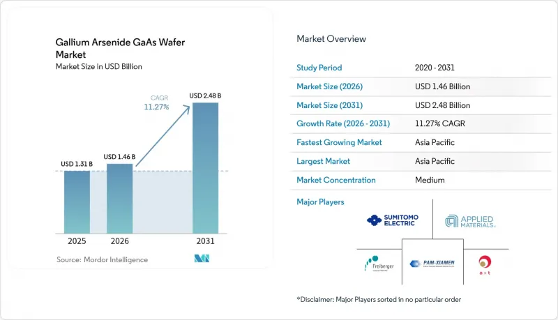
據 Mordor Intelligence 稱,砷化鎵 (GaAs) 晶圓市場預計到 2026 年價值 14.6 億美元,高於 2025 年的 13.1 億美元,預計到 2031 年將達到 24.8 億美元。
預計從 2026 年到 2031 年,其複合年成長率將達到 11.27%。
本報告按應用領域(射頻電子、其他)、晶圓直徑(2吋、3吋、4吋、其他)、生長技術(LEC、VGF、其他)、終端用戶產業(通訊/5G基礎設施、其他)、導電類型(半絕緣GaAs、半導體GaAs)和地區(北美、其他)進行細分。市場預測以美元計價。
全球砷化鎵(GaAs)晶圓市場趨勢及洞察
5G基礎設施部署正在推動對砷化鎵射頻技術的需求。
電信業者正在部署高密度 5G大型基地台和小型基地台基地台,這需要功率放大器能夠在遠高於 28GHz 的頻率範圍內保持線性輸出,而矽 LDMOS 在該頻率範圍內性能會下降。砷化鎵晶圓可實現約 8,500 cm²/V*s 的電子遷移率,從而能夠製造出高效的前端模組,在大規模 MIMO 陣列中保持訊號完整性,確保都市區覆蓋。網路供應商已與垂直整合的砷化鎵製造商簽署了多年供應協議,將 4G 硬體的更新換代週期轉變為可預測的需求,直至 2027 年。
光電裝置(VCSEL、雷射)的蓬勃發展
超大規模資料中心正在向採用基於砷化鎵(GaAs)垂直腔面發射雷射(VCSEL)陣列的400G和800G光纖通訊設備過渡,以實現低延遲和低功耗。智慧型手機製造商正在將VCSEL整合到生物識別模組中用於3D感測,而汽車OEM廠商則將GaAs雷射用於雷射雷達(LiDAR)。外延再生技術的進步提高了散熱性能,延長了裝置壽命,並維持了晶圓的高平均售價(ASP)。
與Si/SiC相比,製造成本更高
提取砷化鎵晶體需要在加壓砷化氣體環境下進行,並且需要處理有毒氣體,因此與矽相比,其資本支出(CapEx)和營運成本(Opex)更高。在4吋和6吋晶圓等較小尺寸的晶圓上,就「每片晶圓晶片數量」而言,砷化鎵的經濟性無法與300毫米矽晶圓相媲美,這限制了砷化鎵在價格敏感型消費性電子產品中的應用。
細分市場分析
到2025年,射頻(RF)電子產品將佔砷化鎵(GaAs)晶圓銷售額的43.65%,因為功率放大器和開關仍然是5G基礎設施升級的核心。隨著高密度小型基地台的規劃,預計這一佔有率將穩定成長。受VCSEL互連和AR/VR光學元件的驅動,光電和成像元件預計將以13.25%的複合年成長率成長,超過所有其他應用,這可能會重塑未來砷化鎵(GaAs)晶圓市場的出貨量格局。
隨著智慧型手機製造商整合基於VCSEL的臉部認證模組,跨領域需求溢出效應正在發生,推動了通用6吋外延線上的光電和射頻元件的生產。雖然基於GaAs的太陽能電池目前仍主要應用於太空船等小眾市場,但異質整合這項新概念有望將多結設計引入地面聚光陣列。
儘管4吋基板憑藉成熟的生產設施仍佔35.85%的銷售額,但產能報告顯示,6吋生產線將以12.85%的複合年成長率(CAGR)消化大部分新增需求。隨著固定成本的分攤和單次生產晶片數量的增加,預計這一轉變將降低砷化鎵(GaAs)晶圓市場的平均售價(ASP)。
隨著產品尺寸擴大到6吋以上,設備供應商正在努力控制溫度梯度和砷蒸氣。最初的8吋試生產已顯示出令人鼓舞的結果,但在商業化部署之前,仍需進一步降低缺陷率。
區域分析
預計到2025年,亞太地區將佔據全球砷化鎵(GaAs)晶圓市場60.10%的佔有率,主要得益於該地區外延生產線的集中分佈、強大的分包基礎以及政府主導的5G基礎設施建設。政府激勵措施正在推動中國當地化合物半導體晶圓廠的擴張,而台灣和韓國則透過代工和設備領域的協同效應,加強了供應鏈多元化。
北美位居第二,這主要得益於航太和國防領域的需求,而該領域需要穩定的國內生產。近期《晶片工業與生產法案》(CHIPS Act)的獎勵為新建晶體生長爐和專用於雷達和衛星專案半絕緣材料的無塵室提供了資金,從而鞏固了長期的國內供應系統。
歐洲在汽車和工業自動化領域依然保持強勁勢頭。一級供應商正在採購砷化鎵功率裝置,以支援高級駕駛輔助系統(ADAS)雷達和工廠感測技術;同時,嚴格的環境指令正在推動晶圓回收利用的循環經濟研究。歐盟協調一致的資金支持一條150毫米化合物半導體晶圓試點生產線,旨在縮小與亞洲的產能差距。
其他好處
- Excel格式的市場預測(ME)表
- 3個月的分析師支持
目錄
第1章:引言
- 研究假設和市場定義
- 調查範圍
第2章:調查方法
第3章執行摘要
第4章 市場狀況
- 市場概覽
- 市場促進因素
- 5G基礎設施的部署正在推動對GaAs射頻元件的需求。
- 光電裝置(VCSEL、雷射)的蓬勃發展
- 航太和國防領域高頻雷達的應用
- 由於亞洲外延生產能力的擴大,供應量增加,平均售價(ASP)降低。
- 微型LED在AR/VR穿戴裝置的應用
- 透過遠端外延技術實現基板重複利用,從而降低晶圓成本
- 市場限制因素
- 與Si/SiC相比,製造成本更高
- 鎵供應集中度和出口限制
- 射頻/功率領域氮化鎵與碳化矽的競爭
- 環境與安全合規性
- 產業價值鏈分析
- 監理情勢
- 技術展望
- 波特五力分析
第5章 市場規模與成長預測
- 透過使用
- 射頻(RF)電子元件
- 光和紅外線LED
- 太陽能發電/太陽能電池
- 光電成像設備
- 其他
- 依晶圓直徑
- 2 吋(50 毫米)
- 3吋(76毫米)
- 4吋(100毫米)
- 6吋(150毫米)
- 8吋(200毫米)或以上
- 透過成長技術
- 液填充柴可拉斯基法(LEC)
- 垂直梯度凍結(VGF)
- 水平布里奇曼法(HB)
- 分子束外延(MBE)
- 金屬有機化學氣相沉積(MOCVD)
- 按最終用途行業分類
- 通訊和5G基礎設施
- 家用電子產品
- 航太/國防
- 汽車(ADAS、電動車)
- 工業和能源
- 導電類型
- 半絕緣GaAs
- 半導體GaAs(n型/p型)
- 按地區
- 北美洲
- 美國
- 加拿大
- 墨西哥
- 南美洲
- 巴西
- 阿根廷
- 其他南美國家
- 歐洲
- 德國
- 英國
- 法國
- 義大利
- 其他歐洲國家
- 亞太地區
- 中國
- 日本
- 韓國
- 印度
- 其他亞太國家
- 中東
- 沙烏地阿拉伯
- 阿拉伯聯合大公國
- 其他中東國家
- 非洲
- 南非
- 其他非洲地區
- 北美洲
第6章 競爭情勢
- 市場集中度
- 策略趨勢
- 市佔率分析
- 公司簡介
- AXT Inc.
- China Crystal Technologies Co. Ltd.
- Freiberger Compound Materials GmbH
- Semiconductor Wafer Inc.
- Sumitomo Electric Industries, Ltd.
- Xiamen Powerway Advanced Material Co., Ltd.
- Wafer Technology Ltd.
- Vital Materials Co., Ltd.
- DOWA Electronics Materials Co., Ltd.
- American Elements, Inc.
- IQE plc
- WIN Semiconductors Corp.
- Advanced Wireless Semiconductor Co.
- Visual Photonics Epitaxy Co., Ltd.(VPEC)
- IntelliEPI, Inc.
- Global Communication Semiconductors, LLC
- Roditi Ltd.
- Veeco Instruments Inc.
- Applied Materials, Inc.
- AIXTRON SE
第7章 市場機會與未來展望
According to Mordor Intelligence, gallium arsenide wafer market size in 2026 is estimated at USD 1.46 billion, growing from 2025 value of USD 1.31 billion with 2031 projections showing USD 2.48 billion, growing at 11.27% CAGR over 2026-2031.
This report is Segmented by Application (Radio-Frequency Electronics, and More), Wafer Diameter (2 Inch, 3 Inch, 4 Inch, and More), Growth Technology (LEC, VGF, and More), End-Use Industry (Telecom and 5G Infrastructure, and More), Conductivity Type (Semi-Insulating GaAs, Semi-Conducting GaAs), and Geography (North America, and More). The Market Forecasts are Provided in Terms of Value (USD).
Global Gallium Arsenide GaAs Wafer Market Trends and Insights
5G Infrastructure Roll-out Fuels GaAs RF Demand
Telecom operators are deploying dense 5G macro- and small-cell sites that require power amplifiers sustaining linear output well above 28 GHz, where silicon LDMOS falters. Gallium arsenide wafers deliver electron mobility around 8,500 cm2/V*s, enabling efficient front-end modules that preserve signal integrity in massive-MIMO arrays for urban coverage. Network vendors lock multiyear supply contracts with vertically integrated GaAs houses, converting 4G hardware refresh cycles into predictable demand through 2027.
Optoelectronic Device Boom (VCSELs, Lasers)
Hyperscale data centers move to 400G and 800G optics that rely on GaAs-based VCSEL arrays for lower latency and power draw. Smartphone makers embed 3D-sensing VCSELs in biometric modules, while automotive OEMs adopt GaAs lasers for LiDAR. Epitaxial regrowth advances improve thermal dissipation, extending device lifetimes and sustaining premium wafer ASPs.
High Production Cost vs Si and SiC
GaAs crystal pulling needs pressurized arsenic atmospheres and toxic-gas handling that raise CapEx and Opex above silicon. Smaller 4-inch and 6-inch formats cannot match the die-per-wafer economics of 300 mm silicon, limiting GaAs uptake in price-sensitive consumer gadgets.
Other drivers and restraints analyzed in the detailed report include:
- Aerospace and Defense Uptake for High-Frequency Radar
- Asian Epitaxy Capacity Boosts Supply and Lowers ASP
- Gallium Supply Concentration and Export Controls
For complete list of drivers and restraints, kindly check the Table Of Contents.
Segment Analysis
RF electronics held 43.65% revenue in 2025 as power amplifiers and switches remain core to 5G infrastructure upgrades. This portion of the Gallium arsenide wafer market size is forecast to climb steadily alongside small-cell densification plans. Photonic and imaging devices, propelled by VCSEL interconnects and AR/VR optics, are set to outpace all other uses at 13.25% CAGR, thereby reshaping future volumes of the Gallium arsenide wafer market.
Cross-segment pull-through emerges as handset makers integrate VCSEL-based face ID modules, boosting both photonics and RF volume on common 6-inch epi lines. Solar cells on GaAs remain a niche for spacecraft, yet new heterointegration concepts could push multi-junction designs into terrestrial concentrator arrays.
Four-inch substrates still command 35.85% revenue thanks to mature tooling, but capacity announcements reveal that 6-inch lines will absorb most incremental demand at 12.85% CAGR. The shift improves die counts per run and spreads fixed costs, nudging the overall Gallium arsenide wafer market toward lower ASPs.
Equipment vendors tackle thermal-gradient control and arsenic vapor management to scale beyond 6 inches. Early 8-inch pilot runs show promise yet require further defect reduction before commercial deployment.
Complete Report Scope:
- By Application
- Radio-Frequency Electronics
- Optical and IR LEDs
- Photovoltaic / Solar Cells
- Photonic and Imaging Devices
- Other Applications
- By Wafer Diameter
- 2 inch (50 mm)
- 3 inch (76 mm)
- 4 inch (100 mm)
- 6 inch (150 mm)
- 8 inch (200 mm) and Above
- By Growth Technology
- Liquid-Encapsulated Czochralski (LEC)
- Vertical Gradient Freeze (VGF)
- Horizontal Bridgman (HB)
- Molecular Beam Epitaxy (MBE)
- Metal-Organic CVD (MOCVD)
- By End-Use Industry
- Telecom and 5G Infrastructure
- Consumer Electronics
- Aerospace and Defense
- Automotive (ADAS, EV)
- Industrial and Energy
- By Conductivity Type
- Semi-insulating GaAs
- Semi-conducting GaAs (n-/p-type)
- By Geography
- North America
- United States
- Canada
- Mexico
- South America
- Brazil
- Argentina
- Rest of South America
- Europe
- Germany
- United Kingdom
- France
- Italy
- Rest of Europe
- Asia-Pacific
- China
- Japan
- South Korea
- India
- Rest of Asia-Pacific
- Middle East
- Saudi Arabia
- United Arab Emirates
- Rest of Middle East
- Africa
- South Africa
- Rest of Africa
- North America
Geography Analysis
Asia-Pacific held 60.10% of the Gallium arsenide wafer market in 2025 thanks to clustered epitaxial lines, a deep subcontract base, and state-backed 5G build-outs. Government incentives help mainland China expand compound-semiconductor fabs, while Taiwan and South Korea provide foundry and equipment synergies that reinforce supply diversity.
North America ranks second, anchored by aerospace and defense demand requiring secure on-shore production. Recent CHIPS Act incentives finance new crystal-growth reactors and cleanrooms dedicated to semi-insulating material for radar and satellite programs, cementing long-term domestic supply.
Europe retains strength in automotive and industrial automation. Tier-1 suppliers source GaAs power devices to support ADAS radar and factory sensing, while stringent environmental directives spur circular-economy research on wafer reclamation. Coordinated EU funding backs pilot lines for 150 mm compound-semiconductor substrates, seeking to narrow the capacity gap with Asia.
- AXT Inc.
- China Crystal Technologies Co. Ltd.
- Freiberger Compound Materials GmbH
- Semiconductor Wafer Inc.
- Sumitomo Electric Industries, Ltd.
- Xiamen Powerway Advanced Material Co., Ltd.
- Wafer Technology Ltd.
- Vital Materials Co., Ltd.
- DOWA Electronics Materials Co., Ltd.
- American Elements, Inc.
- IQE plc
- WIN Semiconductors Corp.
- Advanced Wireless Semiconductor Co.
- Visual Photonics Epitaxy Co., Ltd. (VPEC)
- IntelliEPI, Inc.
- Global Communication Semiconductors, LLC
- Roditi Ltd.
- Veeco Instruments Inc.
- Applied Materials, Inc.
- AIXTRON SE
Additional Benefits:
- The market estimate (ME) sheet in Excel format
- 3 months of analyst support
TABLE OF CONTENTS
1 INTRODUCTION
- 1.1 Study Assumptions and Market Definition
- 1.2 Scope of the Study
2 RESEARCH METHODOLOGY
3 EXECUTIVE SUMMARY
4 MARKET LANDSCAPE
- 4.1 Market Overview
- 4.2 Market Drivers
- 4.2.1 5G infrastructure roll-out fuels GaAs RF demand
- 4.2.2 Optoelectronic device boom (VCSELs, lasers)
- 4.2.3 Aerospace and defense uptake for high-freq radar
- 4.2.4 Asian epitaxy capacity boosts supply and lowers ASP
- 4.2.5 Micro-LED adoption in AR/VR wearables
- 4.2.6 Remote-epitaxy substrate reuse cuts wafer cost
- 4.3 Market Restraints
- 4.3.1 High production cost vs Si and SiC
- 4.3.2 Gallium supply concentration and export controls
- 4.3.3 GaN and SiC competition in RF / power
- 4.3.4 Environmental and safety compliance
- 4.4 Industry Value Chain Analysis
- 4.5 Regulatory Landscape
- 4.6 Technological Outlook
- 4.7 Porter's Five Forces Analysis
- 4.7.1 Bargaining Power of Suppliers
- 4.7.2 Bargaining Power of Buyers
- 4.7.3 Threat of New Entrants
- 4.7.4 Threat of Substitute Products
- 4.7.5 Intensity of Competitive Rivalry
5 MARKET SIZE AND GROWTH FORECASTS (VALUE)
- 5.1 By Application
- 5.1.1 Radio-Frequency Electronics
- 5.1.2 Optical and IR LEDs
- 5.1.3 Photovoltaic / Solar Cells
- 5.1.4 Photonic and Imaging Devices
- 5.1.5 Other Applications
- 5.2 By Wafer Diameter
- 5.2.1 2 inch (50 mm)
- 5.2.2 3 inch (76 mm)
- 5.2.3 4 inch (100 mm)
- 5.2.4 6 inch (150 mm)
- 5.2.5 8 inch (200 mm) and Above
- 5.3 By Growth Technology
- 5.3.1 Liquid-Encapsulated Czochralski (LEC)
- 5.3.2 Vertical Gradient Freeze (VGF)
- 5.3.3 Horizontal Bridgman (HB)
- 5.3.4 Molecular Beam Epitaxy (MBE)
- 5.3.5 Metal-Organic CVD (MOCVD)
- 5.4 By End-Use Industry
- 5.4.1 Telecom and 5G Infrastructure
- 5.4.2 Consumer Electronics
- 5.4.3 Aerospace and Defense
- 5.4.4 Automotive (ADAS, EV)
- 5.4.5 Industrial and Energy
- 5.5 By Conductivity Type
- 5.5.1 Semi-insulating GaAs
- 5.5.2 Semi-conducting GaAs (n-/p-type)
- 5.6 By Geography
- 5.6.1 North America
- 5.6.1.1 United States
- 5.6.1.2 Canada
- 5.6.1.3 Mexico
- 5.6.2 South America
- 5.6.2.1 Brazil
- 5.6.2.2 Argentina
- 5.6.2.3 Rest of South America
- 5.6.3 Europe
- 5.6.3.1 Germany
- 5.6.3.2 United Kingdom
- 5.6.3.3 France
- 5.6.3.4 Italy
- 5.6.3.5 Rest of Europe
- 5.6.4 Asia-Pacific
- 5.6.4.1 China
- 5.6.4.2 Japan
- 5.6.4.3 South Korea
- 5.6.4.4 India
- 5.6.4.5 Rest of Asia-Pacific
- 5.6.5 Middle East
- 5.6.5.1 Saudi Arabia
- 5.6.5.2 United Arab Emirates
- 5.6.5.3 Rest of Middle East
- 5.6.6 Africa
- 5.6.6.1 South Africa
- 5.6.6.2 Rest of Africa
- 5.6.1 North America
6 COMPETITIVE LANDSCAPE
- 6.1 Market Concentration
- 6.2 Strategic Moves
- 6.3 Market Share Analysis
- 6.4 Company Profiles (includes Global level Overview, Market level overview, Core Segments, Financials as available, Strategic Information, Market Rank/Share, Products and Services, Recent Developments)
- 6.4.1 AXT Inc.
- 6.4.2 China Crystal Technologies Co. Ltd.
- 6.4.3 Freiberger Compound Materials GmbH
- 6.4.4 Semiconductor Wafer Inc.
- 6.4.5 Sumitomo Electric Industries, Ltd.
- 6.4.6 Xiamen Powerway Advanced Material Co., Ltd.
- 6.4.7 Wafer Technology Ltd.
- 6.4.8 Vital Materials Co., Ltd.
- 6.4.9 DOWA Electronics Materials Co., Ltd.
- 6.4.10 American Elements, Inc.
- 6.4.11 IQE plc
- 6.4.12 WIN Semiconductors Corp.
- 6.4.13 Advanced Wireless Semiconductor Co.
- 6.4.14 Visual Photonics Epitaxy Co., Ltd. (VPEC)
- 6.4.15 IntelliEPI, Inc.
- 6.4.16 Global Communication Semiconductors, LLC
- 6.4.17 Roditi Ltd.
- 6.4.18 Veeco Instruments Inc.
- 6.4.19 Applied Materials, Inc.
- 6.4.20 AIXTRON SE
7 MARKET OPPORTUNITIES AND FUTURE OUTLOOK
- 7.1 White-space and Unmet-need Assessment

 GaAs晶圓市場:全球產業分析、市場規模、市佔率及2026年至2033年預測(依晶圓類型、應用、最終用戶、國家及地區分類)晶圓凸塊加工服務市場報告:趨勢、預測與競爭分析(至2035年)
 磷酸銦晶片:市場佔有率分析、產業趨勢與統計、成長預測(2026-2031)
 砷化鎵晶片市場:2026-2032年全球市場預測(按摻雜、直徑、晶片類型、應用和銷售管道分類)優質拋光晶圓:市場佔有率分析、行業趨勢和統計數據、成長預測(2026-2031 年)光學熱測量系統市場:依產品類型、技術、應用、最終用戶和銷售管道,全球預測,2026-2032年全球α-氧化鋁市場(依產品類型、粒徑、終端用途產業及通路分類)預測(2026-2032年)
 全球砷化鎵晶片市場規模、佔有率、趨勢和成長分析報告(2026-2034年)晶圓清洗設備市場:2026-2032年全球預測(按設備類型、晶圓尺寸、基板材料、應用和最終用戶分類)晶圓載體清洗機市場按自動化程度、技術、清洗介質、純度、應用和最終用戶分類-2026-2032年全球預測