


 |
市場調查報告書
商品編碼
2123026
磷酸銦晶片:市場佔有率分析、產業趨勢與統計、成長預測(2026-2031)Indium Phosphide Wafer - Market Share Analysis, Industry Trends & Statistics, Growth Forecasts (2026 - 2031) |
||||||

※ 本網頁內容可能與最新版本有所差異。詳細情況請與我們聯繫。
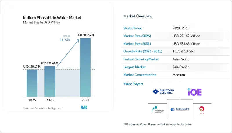
根據 Mordor Intelligence 預測,磷化銦晶片市場將從 2025 年的 1.9817 億美元成長到 2026 年的 2.2142 億美元,到 2031 年將達到 3.8565 億美元,2026 年至 2031 年的複合年成長率為 11.1.1.1.1. 1.1.
本報告按直徑(50.8毫米、76.2毫米及其他)、晶圓摻雜類型(未摻雜導電晶圓及其他)、應用領域(光電/光收發器及其他)、終端用戶行業(電訊/資料通訊及其他)、製造技術(採用VGF方法製造的體晶圓及其他)和地區(北美、南美及其他)進行細分。市場預測以美元計價。
全球磷酸銦晶片市場趨勢及洞察
高速光收發器日益成長的需求正在加速 InP 的應用。
雲端服務供應商正朝著 800G 和 1.6T 連結邁進,這需要能夠以所需速度運行的邊發射雷射和光電二極體,而只有磷化銦 (InP) 才能滿足這些需求。相干公司 (Coherent) 在 2024 年第四季將其 InP 裝置產量提高了三倍,目前已開始提供 3.2T 收發器的樣品。 Source Photonics 公司展示了一款採用 InP 基底組件的 1.6T連貫模組,證實了該材料在共封裝光學元件中的關鍵作用。隨著開關 ASIC 向 51T頻寬發展,可插拔光學元件正被板載雷射引擎所取代,從而降低了磷化銦晶圓市場對基板的需求。
5G基礎設施的部署正在推動對毫米波技術的需求。
商用 5G回程傳輸的工作頻率高於 28GHz,在該頻段,InP HBT 的截止頻率可超過 450GHz,擊穿電壓可超過 4.5V。諾基亞以 23 億美元收購 Infinera,獲得了傳輸節點的 InP連貫技術的專業知識。早期探索兆赫頻率的 6G 測試平台正在使用檢驗高達 610GHz 的 InP HEMT。因此,磷化銦晶圓市場基板的需求不斷成長,不僅用於光前端,也用於射頻鏈路。
供應鏈脆弱性所帶來的穩定威脅
中國於2024年擴大對含銦化合物的出口限制,加劇了價格波動和前置作業時間的不確定性。儘管歐美晶圓製造商目前正在認證鎵和磷的替代供應商,但實現原料自給自足仍需時日。相干公司的CHIPS專案在一定程度上緩解了風險,但短期採購壓力正對整個磷化銦晶圓市場的利潤率構成擠壓。
細分市場分析
2025年,100毫米級晶圓仍將佔據磷化銦晶圓市場43.72%的佔有率,主要滿足主流收發器產品線對成本和良率平衡的需求。諾基亞採用AIXTRON G10-AsP反應器的6吋試點生產線正在推動向150毫米基板的過渡。預計150毫米磷化銦晶圓市場將以13.15%的複合年成長率成長,縮小與砷化鎵晶圓的成本差距。然而,超過6英吋後,機械強度會顯著降低,限制了尺寸的進一步增加。 76.2毫米晶圓在對厚度均勻性要求嚴格的特種光電領域中仍然發揮著至關重要的作用。
擴大大直徑晶圓的生產取決於對專為低模量晶體設計的載片器和邊緣夾持設備的投資。相干公司在德克薩斯州的擴建計畫將採用自動化處理來減少破損,並力爭超過 85% 的優質晶圓良率。同時,50.8 毫米晶圓仍廣泛應用於大學的研究和開發領域,因為升級設備的成本極為高。因此,到 2031 年,磷化銦晶圓市場將同時存在多種直徑規格的晶圓。
到2025年,未摻雜導電基板將以36.18%的市場佔有率佔據主導地位,為光子積體電路的外延生長提供支援。隨著5G射頻功率放大器(需要基板隔離以實現低雜訊)需求的成長,半絕緣鐵(Fe)摻雜晶圓預計將以12.93%的複合年成長率成長。 N型錫(Sn)摻雜和P型鋅(Zn)摻雜晶圓主要用於HEMT和HBT元件,但與用於射頻前端應用的磷化銦晶圓市場中鐵(Fe)摻雜晶圓的成長相比,它們的產量仍然較小。
在兆赫積體電路研究中,背景摻雜濃度對300 GHz增益的影響是研究的重點。費迪南德·布勞恩研究所的異質接面雙極電晶體(HBT)透過最佳化鋅補償,實現了超過450 GHz的運作頻率(fT),凸顯了基板摻雜分佈如何支持系統級技術的進步。量子光電實驗室對超高純度、未摻雜晶圓的需求日益成長,但這些晶圓的價格可能高達標準導電級晶圓的三倍,導致價格彈性有限。
區域分析
預計到2025年,亞太地區將佔全球銷售額的41.55%,複合年成長率(CAGR)為12.41%。日本JX Nippon Mining & Metals已建立起精煉銦和磷原料的垂直整合供應體系,而台灣的Visual Photonics Epitaxy正在擴大用於資料通訊通訊雷射的100毫米晶圓的生產。韓國的先進材料生態系統為MOCVD製程提供耗材,增強了區域流動性。然而,由於中國原料法規的複雜性,出口許可證的核准流程也較為複雜,這為日韓生產商帶來了避險的需求,他們或許能夠在磷化銦晶圓市場獲得溢價。
北美市場佔有率受益於聯邦政府的獎勵。相干公司(Coherent)獲得的3,300萬美元CHIPS津貼擴大了其位於德克薩斯州的150毫米生產線的產能,從而保障了量子計算和國防領域的供應鏈。麻省理工學院林肯實驗室等高校正在研發用於低溫量子位元控制的InP-on-Si發射器原型,為未來的商業性需求創造了條件。然而,國內原料對海外供應的依賴仍是成本結構的一大挑戰。
歐洲正充分利用其在光電的深厚專業知識,尤其是在德國和荷蘭。費迪南德·布勞恩研究所正與弗勞恩霍夫IZM研究所合作,共同設計用於兆赫的InP HBT,而SMART Photonics公司則致力於推廣基於InP的光子積體電路(PIC)代工服務。弗賴貝格化合物材料公司提供的VGF晶圓位錯密度低於1e4cm-2,其設計已應用於量子通訊先導計畫。歐盟的研究津貼正在彌補資本投入,但能源價格的波動正在擠壓利潤空間,使其無法與亞洲競爭對手匹敵,重塑了磷化銦晶圓市場的競爭格局。
其他好處
- Excel格式的市場預測(ME)表
- 3個月的分析師支持
目錄
第1章:引言
- 研究假設和市場定義
- 調查範圍
第2章:調查方法
第3章執行摘要
第4章 市場狀況
- 市場概覽
- 市場促進因素
- 對高速光收發器(400G/800G/1.6T)的需求
- 5G 和下一代 6G回程傳輸基礎設施的部署
- 消費者對用於智慧型手機和穿戴式裝置的短波紅外線感測技術的興趣日益濃厚。
- 透過量子光電研究與發展計劃加快對 InP PIC 的資助
- 將國防相關的紅外線成像技術帶回日本的趨勢正在擴大國內對 InP基板的需求。
- 為了利用閒置的 6 吋 GaAs 生產線,我們將過渡到 6 吋 InP基板。
- 市場限制因素
- 與Si/GaAs替代材料相比,晶圓成本較高
- 鎵/磷的出口限制以及供應鏈對價格波動的脆弱性。
- 尺寸大於 6 英吋的晶圓由於機械脆弱性而導致良率受限。
- 採用矽光電混合雷射平台,減少純InP晶圓的使用。
- 產業價值鏈分析
- 監理情勢
- 技術展望
- 波特五力分析
第5章 市場規模與成長預測
- 依直徑
- 50.8mm
- 76.2mm
- 100mm
- 150毫米或以上
- 晶圓摻雜類型
- 非摻雜導電材料
- N型(S/Sn摻雜)
- P型(鋅摻雜)
- 半絕緣(鐵摻雜)
- 透過使用
- 光電和光收發器
- 射頻和毫米波裝置(HEMT、HBT)
- 太陽能發電和功率轉換
- 量子和特殊感測
- 按最終用戶行業分類
- 電訊和資料通訊
- 家用電器和穿戴設備
- 航太/國防
- 汽車和運輸業
- 醫學與生命科學
- 透過製造技術
- 採用VGF方法製造的大塊晶圓
- 採用LEC/tCZ方法生長的體晶片
- 在矽上進行InP外延生長(混合)
- 用於 MBE/MOCVD 的外延相容基板
- 按地區
- 北美洲
- 美國
- 加拿大
- 墨西哥
- 南美洲
- 巴西
- 阿根廷
- 其他南美國家
- 歐洲
- 德國
- 英國
- 法國
- 義大利
- 其他歐洲國家
- 亞太地區
- 中國
- 日本
- 韓國
- 印度
- 其他亞太國家
- 中東
- 沙烏地阿拉伯
- 阿拉伯聯合大公國
- 其他中東國家
- 非洲
- 南非
- 其他非洲地區
- 北美洲
第6章 競爭情勢
- 市場集中度
- 策略趨勢
- 市佔率分析
- 公司簡介
- Sumitomo Electric Semiconductor Materials, Inc.
- AXT, Inc.
- Freiberger Compound Materials GmbH
- Xiamen Powerway Advanced Material Co., Ltd.
- IQE plc
- II-VI Incorporated(Coherent Corp.)
- JX Nippon Mining & Metals Corporation
- Semiconductor Wafer, Inc.
- Visual Photonics Epitaxy Co., Ltd.(VPEC)
- IntellEPI
- VIGO Photonics SA
- Western Minmetals(SC)Corporation
- PAM-XIAMEN(Powerway Wafer)
- SHANGHAI FAMOUS TRADE CO., LTD(ZMKJ)
- Atecom Technology Co., Ltd.
- Ding Ten Industrial Inc.
- Logitech Ltd.
- LandMark Optoelectronics Corporation
- Epihouse Optoelectronics Co., Ltd.
- Century Goldray Semiconductor Co., Ltd.
第7章 市場機會與未來展望
According to Mordor Intelligence, the indium phosphide wafer market size is expected to grow from USD 198.17 million in 2025 to USD 221.42 million in 2026 and is forecast to reach USD 385.65 million by 2031 at 11.73% CAGR over 2026-2031.
This report is Segmented by Diameter (50. 8mm, 76. 2mm, and More), Wafer Doping Type (Undoped Conductive, and More), Application (Photonics and Optical Transceivers, and More), End-User Industry (Telecommunications and Datacom, and More), Manufacturing Technology (VGF-Grown Bulk, and More), and Geography (North America, South America, and More). The Market Forecasts are Provided in Terms of Value (USD).
Global Indium Phosphide Wafer Market Trends and Insights
High-speed optical-transceiver demand accelerates InP adoption
Cloud operators moving to 800 G and 1.6 T links require edge-emitting lasers and photodiodes that only indium phosphide can provide at the required speeds. Coherent tripled its InP-device output in Q4 2024 and is now sampling 3.2 T transceivers. Source Photonics demonstrated a 1.6 T coherent module using InP-based components, validating the material's indispensability for co-packaged optics. As switch ASICs advance toward 51T bandwidth, pluggable optics give way to on-board laser engines, reducing substrate volumes for the indium phosphide wafer market.
5G infrastructure rollout drives millimeter-wave demand
Commercial 5G backhaul operates above 28 GHz, where InP HBTs offer a cutoff frequency of more than 450 GHz and a breakdown voltage of more than 4.5 V. Nokia's USD 2.3 billion purchase of Infinera secures InP coherent expertise for transport nodes. Early 6G testbeds exploring terahertz frequencies rely on InP HEMTs, which have been validated up to 610 GHz. Consequently, substrate demand rises not only for optical front-ends but also for RF chains within the indium phosphide wafer market.
Supply-chain vulnerabilities threaten stability
China's 2024 expansion of export controls to indium-bearing compounds elevated price volatility and lead-time uncertainty. Western wafer makers now qualify alternative gallium and phosphorus suppliers, yet achieving raw-material self-sufficiency cannot be done quickly. Coherent's CHIPS Act project mitigates some risk, but near-term procurement pressure trims margins across the indium phosphide wafer market.
Other drivers and restraints analyzed in the detailed report include:
- Rising consumer SWIR sensing broadens addressable base
- Quantum-photonics R&D spurs specialty substrate demand
- Cost competitiveness limits penetration
For complete list of drivers and restraints, kindly check the Table Of Contents.
Segment Analysis
The 100 mm class retained a 43.72% indium phosphide wafer market share in 2025, catering to mainstream transceiver lines that strike a balance between cost and yield. A shift toward 150 mm substrates is underway, driven by Nokia's 6-inch pilot line utilizing AIXTRON G10-AsP reactors. The indium phosphide wafer market size for 150 mm formats is forecasted to grow at a 13.15% CAGR, narrowing the cost gap with GaAs. Yet, mechanical fragility above 6 inches restrains further scale, so 76.2 mm wafers remain relevant for specialty photonics that demand tight thickness uniformity.
Growth in large-diameter output hinges on investment in carriers and edge-grip tools designed for low-modulus crystals. Coherent's Texas expansion adopts automated handling to reduce breakage, targeting yields of over 85% for prime wafers. Meanwhile, 50.8 mm wafers persist in university R&D, where tooling upgrades are prohibitively expensive. A diverse diameter mix therefore co-exists within the indium phosphide wafer market through 2031.
Undoped conductive substrates led with a 36.18% share in 2025, underpinning photonic-integrated-circuit epitaxy. Semi-insulating Fe-doped wafers are projected to post a 12.93% CAGR, accelerating alongside 5G RF-power amplifiers that require substrate isolation for low noise. N-type Sn-doped and P-type Zn-doped slices target HEMT and HBT devices, but their volumes remain niche compared to Fe-doped growth in the indium phosphide wafer market size for RF front-ends.
Terahertz IC research highlights the impact of background dopant levels on gain at 300 GHz. The Ferdinand-Braun-Institut's HBTs utilized tailored Zn compensation to achieve a frequency of operation (fT) exceeding 450 GHz, underscoring how substrate doping profiles underpin system-level advances. Demand for ultra-pure, undoped wafers rises in quantum-photonics labs, but price elasticity is limited because such wafers can cost three times as much as standard conductive grades.
Complete Report Scope:
- By Diameter
- 50.8 mm
- 76.2 mm
- 100 mm
- 150 mm and Above
- By Wafer Doping Type
- Undoped Conductive
- N-Type (S / Sn-doped)
- P-Type (Zn-doped)
- Semi-insulating (Fe-doped)
- By Application
- Photonics and Optical Transceivers
- RF and mm-Wave Devices (HEMT, HBT)
- Photovoltaics and Power Conversion
- Quantum and Specialty Sensing
- By End-user Industry
- Telecommunications and Datacom
- Consumer Electronics and Wearables
- Aerospace and Defense
- Automotive and Transportation
- Medical and Life-sciences
- By Manufacturing Technology
- VGF-grown Bulk Wafers
- LEC/tCZ-grown Bulk Wafers
- Epitaxial InP-on-Si (Hybrid)
- MBE/MOCVD Epi-ready Substrates
- By Geography
- North America
- United States
- Canada
- Mexico
- South America
- Brazil
- Argentina
- Rest of South America
- Europe
- Germany
- United Kingdom
- France
- Italy
- Rest of Europe
- Asia-Pacific
- China
- Japan
- South Korea
- India
- Rest of Asia-Pacific
- Middle East
- Saudi Arabia
- United Arab Emirates
- Rest of Middle East
- Africa
- South Africa
- Rest of Africa
- North America
Geography Analysis
Asia-Pacific retained 41.55% of revenue in 2025 and is projected to grow at a 12.41% CAGR. Japan's JX Nippon Mining and Metals provides a vertically integrated supply of purified indium and phosphorous feedstock, while Taiwan's Visual Photonics Epitaxy ramps 100 mm output for datacom lasers. Korea's advanced-materials ecosystem supplies MOCVD consumables, reinforcing regional liquidity. However, export-license complexities from China's raw-material controls create hedging demand for Japanese and Korean producers, who can command price premiums within the indium phosphide wafer market.
North America's share benefits from federal incentives. Coherent's USD 33 million CHIPS grant expands 150 mm line capacity in Texas to safeguard quantum-computing and defense supply chains. Universities such as MIT Lincoln Laboratory prototype InP-on-Si emitters for cryogenic qubit control, seeding future commercial pull. Yet domestic raw material dependence on overseas sources still challenges the cost structure.
Europe leverages deep photonics expertise across Germany and the Netherlands. Ferdinand-Braun-Institut collaborates with Fraunhofer IZM to co-design InP HBTs for terahertz radar, while SMART Photonics pushes foundry services for InP-based PICs. Freiberger Compound Materials supplies VGF wafers with <1e4 cm-2 dislocation density, securing design wins in quantum-communication pilots. EU research grants offset capex, but energy-price volatility narrows margins versus Asian peers, shaping competitive dynamics of the indium phosphide wafer market.
- Sumitomo Electric Semiconductor Materials, Inc.
- AXT, Inc.
- Freiberger Compound Materials GmbH
- Xiamen Powerway Advanced Material Co., Ltd.
- IQE plc
- II-VI Incorporated (Coherent Corp.)
- JX Nippon Mining & Metals Corporation
- Semiconductor Wafer, Inc.
- Visual Photonics Epitaxy Co., Ltd. (VPEC)
- IntellEPI
- VIGO Photonics S.A.
- Western Minmetals (SC) Corporation
- PAM-XIAMEN (Powerway Wafer)
- SHANGHAI FAMOUS TRADE CO., LTD (ZMKJ)
- Atecom Technology Co., Ltd.
- Ding Ten Industrial Inc.
- Logitech Ltd.
- LandMark Optoelectronics Corporation
- Epihouse Optoelectronics Co., Ltd.
- Century Goldray Semiconductor Co., Ltd.
Additional Benefits:
- The market estimate (ME) sheet in Excel format
- 3 months of analyst support
TABLE OF CONTENTS
1 INTRODUCTION
- 1.1 Study Assumptions and Market Definition
- 1.2 Scope of the Study
2 RESEARCH METHODOLOGY
3 EXECUTIVE SUMMARY
4 MARKET LANDSCAPE
- 4.1 Market Overview
- 4.2 Market Drivers
- 4.2.1 High-speed optical transceiver demand (400G/800G/1.6T)
- 4.2.2 5G and emerging 6G backhaul infrastructure rollout
- 4.2.3 Rising consumer SWIR sensing in smartphones and wearables
- 4.2.4 Quantum photonics R&D programs accelerating InP PIC funding
- 4.2.5 Defense IR-imaging re-shoring mandates boosting domestic InP substrates
- 4.2.6 Migration to 6-inch InP substrates to leverage idle GaAs 6-inch lines
- 4.3 Market Restraints
- 4.3.1 High wafer cost versus Si/GaAs alternatives
- 4.3.2 Supply-chain exposure to Ga-/P-export controls and price volatility
- 4.3.3 Mechanical fragility limiting yields beyond 6-inch wafers
- 4.3.4 Si-photonics hybrid laser platforms reducing pure InP wafer volumes
- 4.4 Industry Value Chain Analysis
- 4.5 Regulatory Landscape
- 4.6 Technological Outlook
- 4.7 Porter's Five Forces Analysis
- 4.7.1 Bargaining Power of Suppliers
- 4.7.2 Bargaining Power of Buyers
- 4.7.3 Threat of New Entrants
- 4.7.4 Threat of Substitute Products
- 4.7.5 Intensity of Competitive Rivalry
5 MARKET SIZE AND GROWTH FORECASTS (VALUE)
- 5.1 By Diameter
- 5.1.1 50.8 mm
- 5.1.2 76.2 mm
- 5.1.3 100 mm
- 5.1.4 150 mm and Above
- 5.2 By Wafer Doping Type
- 5.2.1 Undoped Conductive
- 5.2.2 N-Type (S / Sn-doped)
- 5.2.3 P-Type (Zn-doped)
- 5.2.4 Semi-insulating (Fe-doped)
- 5.3 By Application
- 5.3.1 Photonics and Optical Transceivers
- 5.3.2 RF and mm-Wave Devices (HEMT, HBT)
- 5.3.3 Photovoltaics and Power Conversion
- 5.3.4 Quantum and Specialty Sensing
- 5.4 By End-user Industry
- 5.4.1 Telecommunications and Datacom
- 5.4.2 Consumer Electronics and Wearables
- 5.4.3 Aerospace and Defense
- 5.4.4 Automotive and Transportation
- 5.4.5 Medical and Life-sciences
- 5.5 By Manufacturing Technology
- 5.5.1 VGF-grown Bulk Wafers
- 5.5.2 LEC/tCZ-grown Bulk Wafers
- 5.5.3 Epitaxial InP-on-Si (Hybrid)
- 5.5.4 MBE/MOCVD Epi-ready Substrates
- 5.6 By Geography
- 5.6.1 North America
- 5.6.1.1 United States
- 5.6.1.2 Canada
- 5.6.1.3 Mexico
- 5.6.2 South America
- 5.6.2.1 Brazil
- 5.6.2.2 Argentina
- 5.6.2.3 Rest of South America
- 5.6.3 Europe
- 5.6.3.1 Germany
- 5.6.3.2 United Kingdom
- 5.6.3.3 France
- 5.6.3.4 Italy
- 5.6.3.5 Rest of Europe
- 5.6.4 Asia-Pacific
- 5.6.4.1 China
- 5.6.4.2 Japan
- 5.6.4.3 South Korea
- 5.6.4.4 India
- 5.6.4.5 Rest of Asia-Pacific
- 5.6.5 Middle East
- 5.6.5.1 Saudi Arabia
- 5.6.5.2 United Arab Emirates
- 5.6.5.3 Rest of Middle East
- 5.6.6 Africa
- 5.6.6.1 South Africa
- 5.6.6.2 Rest of Africa
- 5.6.1 North America
6 COMPETITIVE LANDSCAPE
- 6.1 Market Concentration
- 6.2 Strategic Moves
- 6.3 Market Share Analysis
- 6.4 Company Profiles {(includes Global level Overview, Market level overview, Core Segments, Financials as available, Strategic Information, Market Rank/Share for key companies, Products and Services, and Recent Developments)}
- 6.4.1 Sumitomo Electric Semiconductor Materials, Inc.
- 6.4.2 AXT, Inc.
- 6.4.3 Freiberger Compound Materials GmbH
- 6.4.4 Xiamen Powerway Advanced Material Co., Ltd.
- 6.4.5 IQE plc
- 6.4.6 II-VI Incorporated (Coherent Corp.)
- 6.4.7 JX Nippon Mining & Metals Corporation
- 6.4.8 Semiconductor Wafer, Inc.
- 6.4.9 Visual Photonics Epitaxy Co., Ltd. (VPEC)
- 6.4.10 IntellEPI
- 6.4.11 VIGO Photonics S.A.
- 6.4.12 Western Minmetals (SC) Corporation
- 6.4.13 PAM-XIAMEN (Powerway Wafer)
- 6.4.14 SHANGHAI FAMOUS TRADE CO., LTD (ZMKJ)
- 6.4.15 Atecom Technology Co., Ltd.
- 6.4.16 Ding Ten Industrial Inc.
- 6.4.17 Logitech Ltd.
- 6.4.18 LandMark Optoelectronics Corporation
- 6.4.19 Epihouse Optoelectronics Co., Ltd.
- 6.4.20 Century Goldray Semiconductor Co., Ltd.
7 MARKET OPPORTUNITIES AND FUTURE OUTLOOK
- 7.1 White-space and Unmet-need Assessment

 GaAs晶圓市場:全球產業分析、市場規模、市佔率及2026年至2033年預測(依晶圓類型、應用、最終用戶、國家及地區分類)晶圓凸塊加工服務市場報告:趨勢、預測與競爭分析(至2035年)
 砷化鎵(GaAs)晶片:市場佔有率分析、產業趨勢和統計數據以及成長預測(2026-2031 年)
 砷化鎵晶片市場:2026-2032年全球市場預測(按摻雜、直徑、晶片類型、應用和銷售管道分類)優質拋光晶圓:市場佔有率分析、行業趨勢和統計數據、成長預測(2026-2031 年)光學熱測量系統市場:依產品類型、技術、應用、最終用戶和銷售管道,全球預測,2026-2032年全球α-氧化鋁市場(依產品類型、粒徑、終端用途產業及通路分類)預測(2026-2032年)
 全球砷化鎵晶片市場規模、佔有率、趨勢和成長分析報告(2026-2034年)晶圓清洗設備市場:2026-2032年全球預測(按設備類型、晶圓尺寸、基板材料、應用和最終用戶分類)晶圓載體清洗機市場按自動化程度、技術、清洗介質、純度、應用和最終用戶分類-2026-2032年全球預測