


 |
市場調查報告書
商品編碼
1939646
半導體代工:市場佔有率分析、產業趨勢與統計、成長預測(2026-2031)Semiconductor Foundry - Market Share Analysis, Industry Trends & Statistics, Growth Forecasts (2026 - 2031) |
||||||
※ 本網頁內容可能與最新版本有所差異。詳細情況請與我們聯繫。
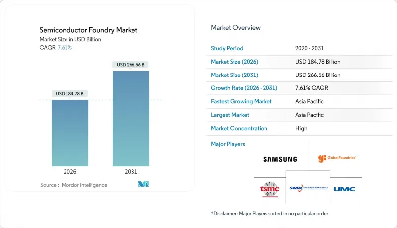
全球半導體代工市場預計到 2026 年將達到 1,847.8 億美元,高於 2025 年的 1,717.2 億美元,預計到 2031 年將達到 2,665.6 億美元。
預計2026年至2031年複合年成長率將達7.61%。
5奈米及以下過程的人工智慧(AI)運算需求激增、成熟製程節點的汽車晶片需求持續成長,以及政府強力的獎勵,共同推動著該產業的技術和地域覆蓋範圍不斷擴大。先進封裝技術,特別是晶片組和3D整合電路(3D IC),正逐漸成為重要的收入來源,但水資源管理、出口限制合規以及極紫外光刻(EUV)設備工程師短缺等挑戰限制了近期產能擴張。日益激烈的地緣政治競爭正推動北美、歐洲和印度等地的製造業在地化,逐漸削弱亞太地區傳統的製造業優勢,儘管其主導地位依然穩固。目前的競爭格局聚焦於5奈米及以下製程節點的領先地位、具成本效益的28奈米製程能力以及面向Start-Ups的代工即服務(FaaS)產品。
全球半導體代工市場趨勢與洞察
面向5奈米以下先進節點的AI加速器競賽
隨著超大規模資料中心業者和晶片設計商競相訓練大規模人工智慧模型,5奈米以下製程的製造能力已從利基市場走向主流。台積電報告稱,2025年第二季度,7奈米及更小工藝的晶圓銷量佔其總銷量的74%,這印證了客戶對密度優勢的重視。三星的2奈米全環柵極製程和英特爾的1.4奈米藍圖凸顯了產業向原子級微型化的轉型。快速的製程節點轉換也加速了對先進中介層的需求,因此需要對晶圓廠和封裝生產線進行協同最佳化。高資本密集度(每個晶圓廠超過200億美元)限制了潛在競爭對手的數量,並鞏固了寡占格局,製程技術優勢直接決定市場佔有率。
汽車電氣化推動主流晶片需求
電動車需要兩卡車的矽:成熟製程節點的電源管理積體電路和尖端製程節點的高效能運算系統級晶片。汽車製造商轉向集中式電子架構,確保了28奈米和45奈米製程的長期產能,為經常受到週期性智慧型手機訂單壓力的晶圓廠提供了可靠的產能補充。漫長的認證週期和嚴格的AEC-Q100標準促使廠商簽訂多年產能預訂契約,從而改善了那些平衡成熟製程節點和先進製程節點的代工廠的收入前景。特斯拉的客製化晶片策略表明,原始設備製造商(OEM)如何利用專用產能合約來確保供應並實現性能差異化。
地緣政治出口管制的不確定性
針對外國直接產品的出口限制,相關規定擴大,限制了先進光刻技術向某些國家的出口,迫使晶圓廠將傳統生產線和先進生產線分開。由於企業需要在多個司法管轄區重複購置設備和審核,合規成本不斷上升。在美國的壓力下,馬來西亞收緊半導體政策,影響波及整個東南亞地區,如今高階GPU的出貨都會引發漫長的授權核准流程。難以預測的監管動態阻礙了新計畫,尤其是5奈米以下過程的項目,從而延緩了短期投資週期。
細分市場分析
截至2025年,28奈米製程節點將佔總收入的59.45%,並構成對成本敏感、大量生產的半導體代工市場規模的基礎。 10奈米以下製程節點雖然出貨量較小,但預計到2031年將以9.05%的複合年成長率成長,這主要得益於人工智慧和高效能運算的需求。這將導致收入結構兩極化:成熟的製程節點將確保汽車和工業領域穩定的現金流,而前緣製程節點則將提供更高的溢價和利潤率。
資本支出紀律仍然至關重要。台積電將於2025年開始試生產其2nm工藝,以確保從智慧型手機和加速器客戶處獲得預付款。英特爾和三星也紛紛推出1.4nm和2nm環柵(GAA)製程開發計劃,加劇了資本競爭。同時,16nm和14nm節點將縮小網路晶片的成本績效差距。傳統的65nm及以上製程將繼續供應長生命週期的類比和射頻設計,即使行動電話需求放緩,也能維持晶圓廠的健康運轉率。
向300毫米製造設備的過渡提高了單次運行的晶粒良率,並減少了邊緣損耗造成的廢棄物,使半導體代工市場到2025年能夠佔據68.10%的市場佔有率。隨著新建晶圓廠將300毫米設備作為40奈米以下製程的標準配置,複合年成長率將持續維持9.42%的年均水準。同時,200毫米製程已在MEMS、功率GaN和專用模擬應用領域中廣泛應用,但這些領域的尺寸縮小和化學特性使得向300毫米製程的過渡充滿挑戰。
規模經濟效應顯著。一旦300毫米晶圓廠的月產能達到10萬片晶圓,在設備折舊免稅額後,其單價可比200毫米晶圓低30%。然而,150億至200億美元的進入門檻限制了新進入者,並鞏固了現有企業的優勢。目前仍有專門的150毫米生產線用於生產碳化矽、砷化鎵以及依賴特殊基板的光電產品。
區域分析
預計到2025年,亞太地區將佔據22.65%的營收佔有率,並在2031年之前以8.44%的複合年成長率成長,這主要得益於台灣無與倫比的先進過程節點密度和韓國垂直整合的產業生態系統。台灣在2025年第二季的營收達到288.7億美元,展現了該地區龐大的生產規模。在出口限制的背景下,中國的中芯國際正專注於28奈米以上製程工藝;而馬來西亞和新加坡則在面臨美國更嚴格的限制時,不斷提升其組裝和測試能力。
在《晶片法案》(CHIPS Act)的推動下,北美正重新崛起為製造地,亞利桑那州、俄亥俄州和紐約州的工廠破土動工,新增了5奈米級和成熟製程節點的產能。聯邦津貼降低了數十億美元計劃的風險,而國防抵銷協議則保障了最低運作。歐洲則專注於汽車級和專用類比晶片,充分利用德國的汽車產業叢集和荷蘭的微影術技術。歐盟的資金規模雖然小規模美國,但目標是到2030年將區域產能翻倍。
在印度、中東和非洲部分地區,該地區正透過對組裝、測試和設計服務的激勵措施來增強自身影響力。印度斥資100億美元的計畫吸引了美光科技27.5億美元的ATMP(組裝、測試和製造流程)項目以及塔塔集團110億美元的待開發區項目,其目標是到2030年使國內需求接近1000億至1100億美元。海灣國家正在考慮建造晶圓代工廠以實現經濟多元化,但水資源限制和技能短缺限制了相關進展。新興全部區域在尋求縮短供應鏈,以規避地緣政治衝擊。
其他福利:
- Excel格式的市場預測(ME)表
- 3個月的分析師支持
目錄
第1章 引言
- 研究假設和市場定義
- 調查範圍
第2章調查方法
第3章執行摘要
第4章 市場情勢
- 市場概覽
- 市場促進因素
- 汽車電氣化推動半導體需求主流化
- 物聯網邊緣的普及需要成熟的節點容量
- 面向5奈米以下先進節點的AI加速器競賽
- 晶片組+3D積體電路需要新的代工流程
- 國防部推廣可靠的國內製造廠
- 面向Start-Ups的代工廠即服務模式
- 市場限制
- 地緣政治出口管制的不確定性
- 通貨膨脹和資本投資的長期投資回收期
- 水資源許可證限制了大型工廠的運營
- 3奈米以下極紫外光刻維護人員短缺
- 產業價值鏈分析
- 監管環境
- 技術展望
- 晶圓廠運轉率趨勢
- 波特五力分析
- 供應商的議價能力
- 買方的議價能力
- 新進入者的威脅
- 替代品的威脅
- 競爭對手之間的競爭
- 宏觀經濟因素如何影響市場
第5章 市場規模與成長預測
- 依技術節點
- 10/7/5 奈米或更小
- 16/14 nm
- 20nm
- 28nm
- 45/40 nm
- 65奈米或以上
- 按晶圓尺寸
- 300 mm
- 200 mm
- 150毫米或更小
- Foundry經營模式
- 全日制
- IDM Foundry 服務
- Fab Light
- 透過使用
- 家用電子電器和通訊設備
- 車
- 工業與物聯網
- 高效能運算(HPC)
- 其他用途
- 按地區
- 北美洲
- 美國
- 加拿大
- 墨西哥
- 南美洲
- 巴西
- 阿根廷
- 南美洲其他地區
- 歐洲
- 德國
- 英國
- 法國
- 義大利
- 其他歐洲地區
- 亞太地區
- 中國
- 日本
- 韓國
- 印度
- 亞太其他地區
- 中東
- 沙烏地阿拉伯
- 阿拉伯聯合大公國
- 其他中東地區
- 非洲
- 南非
- 其他非洲地區
- 北美洲
第6章 競爭情勢
- 市場集中度
- 策略趨勢
- 市佔率分析
- 公司簡介
- Taiwan Semiconductor Manufacturing Co. Ltd.(TSMC)
- Samsung Electronics Co. Ltd.(Samsung Foundry)
- GlobalFoundries Inc.
- United Microelectronics Corp.(UMC)
- Semiconductor Manufacturing International Corp.(SMIC)
- Intel Corp.(Intel Foundry Services)
- Tower Semiconductor Ltd.
- STMicroelectronics NV
- Powerchip Semiconductor Manufacturing Corp.(PSMC)
- Vanguard International Semiconductor Corp.
- Hua Hong Semiconductor Ltd.
- X-FAB Silicon Foundries SE
- ASE Group
- Dongbu HiTek Co. Ltd.
- Renesas Electronics Corp.
- JCET Group
- Amkor Technology
- SkyWater Technology Inc.
- VIS Semiconductor Co. Ltd.
- PSMC Group(Nexchip)
第7章 市場機會與未來展望
The global semiconductor foundry market size in 2026 is estimated at USD 184.78 billion, growing from 2025 value of USD 171.72 billion with 2031 projections showing USD 266.56 billion, growing at 7.61% CAGR over 2026-2031.
A combination of soaring artificial-intelligence compute needs at sub-5 nm, sustained demand for mature-node automotive chips, and intensive government incentives is widening both the technology and geographic footprint of the sector. Advanced packaging, especially chiplets and 3-D ICs, has become a parallel revenue engine, while water stewardship, export-control compliance, and EUV-tool talent shortages temper near-term capacity additions. Intensifying geopolitical competition is prompting North America, Europe, and India to localize fabrication, gradually diffusing Asia-Pacific's traditional production dominance without dislodging its leadership. Competitive dynamics now hinge on node leadership below 5 nm, cost-efficient 28 nm capacity, and foundry-as-a-service offerings targeting start-ups.
Global Semiconductor Foundry Market Trends and Insights
AI Accelerator Race for Less than 5 nm Advanced Nodes
Sub-5 nm capacity has moved from niche to mainstream as hyperscalers and chip designers race to train larger AI models. TSMC reported that 7 nm and finer nodes contributed 74% of wafer revenue in Q2 2025, underscoring the premium customers place on density leadership. Samsung's gate-all-around 2 nm program and Intel's 1.4 nm roadmap confirm an industry-wide pivot toward atomic-scale geometries. Rapid node migration is also fueling demand for advanced interposers, necessitating co-optimized fab and packaging lines. High capital intensity-often above USD 20 billion per fab-limits viable competitors and cements an oligopolistic market where process leadership directly dictates share.
Mainstream Chip Demand from Automotive Electrification
Electric vehicles require dual-track silicon: power-management ICs at mature nodes and high-compute SoCs at leading nodes. Automakers' shift to centralized electronic architectures locks in long-term 28 nm and 45 nm volumes, providing reliable backfill for fabs otherwise pressured by cyclical smartphone orders. Long qualification cycles and strict AEC-Q100 standards encourage multi-year capacity reservations, improving revenue visibility for foundries that balance mature and advanced nodes. Tesla's custom chip strategy illustrates how OEMs use dedicated capacity deals to secure supply and differentiate performance.
Geopolitical Export-Control Uncertainty
Expanded Foreign-Produced Direct Product rules restrict advanced lithography exports to specific countries, forcing fabs to segregate legacy and cutting-edge lines. Compliance costs rise as companies duplicate equipment sets and audits across jurisdictions. Malaysia's tighter chip policies under U.S. pressure show knock-on effects in Southeast Asia, where routing high-end GPUs now triggers lengthy license reviews. Unpredictable rule-making discourages green-field projects, particularly at 5 nm and below, muting near-term investment cycles.
Other drivers and restraints analyzed in the detailed report include:
- Defense Agencies' Push for Trusted Domestic Fabs
- Chiplets + 3-D IC Needing New Foundry Workflows
- Talent Crunch in Sub-3 nm EUV Maintenance
For complete list of drivers and restraints, kindly check the Table Of Contents.
Segment Analysis
In 2025, the 28 nm node generated 59.45% revenue, anchoring the semiconductor foundry market size for cost-sensitive, high-volume devices. Nodes finer than 10 nm, although smaller in shipment volume, will produce a 9.05% CAGR through 2031, reflecting AI and HPC pull-through. Revenue mix therefore bifurcates: mature nodes assure predictable automotive and industrial cash flows, while leading-edge nodes command premium pricing and margins.
Capex discipline remains pivotal. TSMC begins 2 nm risk production in 2025, drawing prepayments from smartphone and accelerator clients. Intel and Samsung respond with 1.4 nm and 2 nm gate-all-around timelines, intensifying capital races. Meanwhile, 16 nm and 14 nm nodes bridge cost-performance gaps for networking silicon. Legacy 65 nm and above still serve analog and RF designs with long lifecycles, keeping fabs running at healthy utilization even when handset demand softens.
The transition to 300 mm tooling lifted die output per run and cut edge-loss waste, enabling the segment to capture 68.10% of the semiconductor foundry market share in 2025. Growth persists at 9.42% CAGR as new fabs select 300 mm equipment by default for anything below 40 nm. In contrast, 200 mm remains entrenched in MEMS, power GaN, and niche analog where geometry or chemistry complicates 300 mm migration.
Economies of scale are stark. A 300 mm fab reaching 100,000 wafers-per-month can undercut 200 mm cost per die by 30% once fully depreciated. Yet the USD 15-20 billion entry fee restricts newcomers, reinforcing incumbent advantage. Specialized 150 mm lines persist for SiC, GaAs, and photonics products that rely on exotic substrates.
The Semiconductor Foundry Market Report is Segmented by Technology Node (10/7/5 Nm and Below, 16/14 Nm, 20 Nm, and More), Wafer Size (300 Mm, 200 Mm, <=150 Mm), Foundry Business Model (Pure-Play, IDM Foundry Services, Fab-Lite), Application (Consumer Electronics and Communication, Automotive, and More), and Geography (North America, South America, Europe, and More). The Market Forecasts are Provided in Terms of Value (USD).
Geography Analysis
Asia-Pacific captured 22.65% revenue in 2025 and is set for an 8.44% CAGR through 2031, propelled by Taiwan's unrivaled advanced-node density and South Korea's vertical integration ecosystems. Taiwan's Q2 2025 revenue of USD 28.87 billion underscores the region's throughput scale. China's SMIC concentrates on 28 nm and above amid export-tool restrictions, while Malaysia and Singapore reinforce assembly and test depth despite tighter U.S. compliance rules.
North America is re-emerging as a fabrication hub under the CHIPS Act, with groundbreakings in Arizona, Ohio, and New York adding both 5 nm class and mature-node capacity. Federal grants de-risk billion-dollar projects, and defense offsets guarantee baseline loadings. Europe focuses on automotive-grade and specialty analog, leveraging Germany's auto cluster and the Netherlands' lithography prowess. EU funding pools, though smaller than U.S. packages, aim to double regional output by 2030.
India, the Middle East, and pockets of Africa are staking claims via assembly, test, and design-service incentives. India's USD 10 billion program attracted Micron's USD 2.75 billion ATMP and Tata's USD 11 billion green-field fab plans, targeting domestic demand approaching USD 100-110 billion by 2030. Gulf countries explore foundries for economic diversification, but water constraints and skills gaps temper speed. Collectively, new geographies aim to shorten supply chains and hedge geopolitical shocks.
- Taiwan Semiconductor Manufacturing Co. Ltd. (TSMC)
- Samsung Electronics Co. Ltd. (Samsung Foundry)
- GlobalFoundries Inc.
- United Microelectronics Corp. (UMC)
- Semiconductor Manufacturing International Corp. (SMIC)
- Intel Corp. (Intel Foundry Services)
- Tower Semiconductor Ltd.
- STMicroelectronics N.V.
- Powerchip Semiconductor Manufacturing Corp. (PSMC)
- Vanguard International Semiconductor Corp.
- Hua Hong Semiconductor Ltd.
- X-FAB Silicon Foundries SE
- ASE Group
- Dongbu HiTek Co. Ltd.
- Renesas Electronics Corp.
- JCET Group
- Amkor Technology
- SkyWater Technology Inc.
- VIS Semiconductor Co. Ltd.
- PSMC Group (Nexchip)
Additional Benefits:
- The market estimate (ME) sheet in Excel format
- 3 months of analyst support
TABLE OF CONTENTS
1 INTRODUCTION
- 1.1 Study Assumptions and Market Definition
- 1.2 Scope of the Study
2 RESEARCH METHODOLOGY
3 EXECUTIVE SUMMARY
4 MARKET LANDSCAPE
- 4.1 Market Overview
- 4.2 Market Drivers
- 4.2.1 Mainstream chip demand from automotive electrification
- 4.2.2 IoT-edge proliferation requiring mature?node capacity
- 4.2.3 AI accelerator race for Less than 5 nm advanced nodes
- 4.2.4 Chiplets + 3D IC needing new foundry workflows
- 4.2.5 Defense agencies push for trusted domestic fabs
- 4.2.6 Foundry-as-a-Service model for start-ups
- 4.3 Market Restraints
- 4.3.1 Geopolitical export-control uncertainty
- 4.3.2 Capex inflation and long pay-back periods
- 4.3.3 Water-use permits limiting mega-fabs
- 4.3.4 Talent crunch in sub-3 nm EUV maintenance
- 4.4 Industry Value Chain Analysis
- 4.5 Regulatory Landscape
- 4.6 Technological Outlook
- 4.7 Foundry Capacity Utilization Trends
- 4.8 Porter's Five Forces Analysis
- 4.8.1 Bargaining Power of Suppliers
- 4.8.2 Bargaining Power of Buyers
- 4.8.3 Threat of New Entrants
- 4.8.4 Threat of Substitutes
- 4.8.5 Intensity of Competitive Rivalry
- 4.9 Impact of Macroeconomic Factors on the Market
5 MARKET SIZE AND GROWTH FORECASTS (VALUE)
- 5.1 By Technology Node
- 5.1.1 10/7/5 nm and below
- 5.1.2 16/14 nm
- 5.1.3 20 nm
- 5.1.4 28 nm
- 5.1.5 45/40 nm
- 5.1.6 65 nm and above
- 5.2 By Wafer Size
- 5.2.1 300 mm
- 5.2.2 200 mm
- 5.2.3 ?150 mm
- 5.3 By Foundry Business Model
- 5.3.1 Pure-play
- 5.3.2 IDM Foundry Services
- 5.3.3 Fab-lite
- 5.4 By Application
- 5.4.1 Consumer Electronics and Communication
- 5.4.2 Automotive
- 5.4.3 Industrial and IoT
- 5.4.4 High-Performance Computing (HPC)
- 5.4.5 Other Applications
- 5.5 By Geography
- 5.5.1 North America
- 5.5.1.1 United States
- 5.5.1.2 Canada
- 5.5.1.3 Mexico
- 5.5.2 South America
- 5.5.2.1 Brazil
- 5.5.2.2 Argentina
- 5.5.2.3 Rest of South America
- 5.5.3 Europe
- 5.5.3.1 Germany
- 5.5.3.2 United Kingdom
- 5.5.3.3 France
- 5.5.3.4 Italy
- 5.5.3.5 Rest of Europe
- 5.5.4 Asia-Pacific
- 5.5.4.1 China
- 5.5.4.2 Japan
- 5.5.4.3 South Korea
- 5.5.4.4 India
- 5.5.4.5 Rest of Asia-Pacific
- 5.5.5 Middle East
- 5.5.5.1 Saudi Arabia
- 5.5.5.2 United Arab Emirates
- 5.5.5.3 Rest of Middle East
- 5.5.6 Africa
- 5.5.6.1 South Africa
- 5.5.6.2 Rest of Africa
- 5.5.1 North America
6 COMPETITIVE LANDSCAPE
- 6.1 Market Concentration
- 6.2 Strategic Moves
- 6.3 Market Share Analysis
- 6.4 Company Profiles (includes Global level Overview, Market level Overview, Core Segments, Financials as available, Strategic Information, Market Rank/Share, Products and Services, Recent Developments)
- 6.4.1 Taiwan Semiconductor Manufacturing Co. Ltd. (TSMC)
- 6.4.2 Samsung Electronics Co. Ltd. (Samsung Foundry)
- 6.4.3 GlobalFoundries Inc.
- 6.4.4 United Microelectronics Corp. (UMC)
- 6.4.5 Semiconductor Manufacturing International Corp. (SMIC)
- 6.4.6 Intel Corp. (Intel Foundry Services)
- 6.4.7 Tower Semiconductor Ltd.
- 6.4.8 STMicroelectronics N.V.
- 6.4.9 Powerchip Semiconductor Manufacturing Corp. (PSMC)
- 6.4.10 Vanguard International Semiconductor Corp.
- 6.4.11 Hua Hong Semiconductor Ltd.
- 6.4.12 X-FAB Silicon Foundries SE
- 6.4.13 ASE Group
- 6.4.14 Dongbu HiTek Co. Ltd.
- 6.4.15 Renesas Electronics Corp.
- 6.4.16 JCET Group
- 6.4.17 Amkor Technology
- 6.4.18 SkyWater Technology Inc.
- 6.4.19 VIS Semiconductor Co. Ltd.
- 6.4.20 PSMC Group (Nexchip)
7 MARKET OPPORTUNITIES AND FUTURE OUTLOOK
- 7.1 White-space and Unmet-need Assessment
 半導體代工廠市場:按代工廠類型、應用和地區分類
 2034年移動出行科技Start-Ups及投資市場預測:經營模式、投資階段、技術及地區分類的全球分析全球半導體晶圓代工廠市場預測至2034年:按類型、晶圓尺寸、服務類型、技術、應用、最終用戶和地區分類
 半導體代工市場規模、佔有率、趨勢和預測:按技術節點、代工類型、應用和地區分類,2026-2034 年鑄造服務市場:依材料、製程、最終用途產業及地區分類
 鑄造服務市場:按工藝、客戶類型和應用分類-2026-2032年全球市場預測
 半導體代工市場規模、佔有率和成長分析:按技術節點尺寸、技術、代工類型、應用和地區分類 - 2026-2033 年行業預測
 半導體代工市場:成長機會、成長要素、產業趨勢分析及2026年至2035年預測全球化合物半導體代工服務市場:預測(至2034年)-按材料類型、晶圓尺寸、裝置類型、技術、應用、最終用戶和地區進行分析
 2026年全球半導體契約製造市場報告