

 |
市場調查報告書
商品編碼
1959558
半導體代工市場:成長機會、成長要素、產業趨勢分析及2026年至2035年預測Semiconductor Foundry Market Opportunity, Growth Drivers, Industry Trend Analysis, and Forecast 2026 - 2035 |
||||||
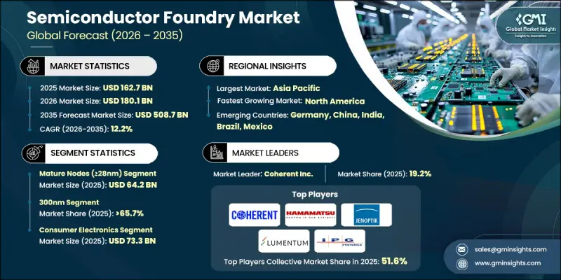
2025 年全球半導體代工市場價值為 1,627 億美元,預計到 2035 年將達到 5,087 億美元,年複合成長率為 12.2%。
半導體代工廠是專門的製造工廠,利用先進的光刻和精密蝕刻工藝,根據無廠半導體公司提供的設計,在矽晶圓上生產積體電路。純代工廠模式專注於製造服務,使客戶能夠加速人工智慧、汽車電子、高效能運算和下一代連接技術領域的創新。對人工智慧驅動系統、電動車和5G基礎設施日益成長的需求,使得企業越來越依賴晶片製造外包。代工廠在提供先進節點、支援即時處理以及在複雜的工業環境中實現自動化方面發揮著至關重要的作用。政府和企業對工業4.0和人工智慧基礎設施的加大投資,進一步加速了產能的擴張。隨著各行業對日益複雜和節能的半導體產品的需求不斷成長,半導體代工廠市場也持續擴展其技術能力和全球生產基地,以支持長期的數位轉型舉措。
| 市場範圍 | |
|---|---|
| 開始年份 | 2025 |
| 預測年份 | 2026-2035 |
| 起始值 | 1627億美元 |
| 預測金額 | 5087億美元 |
| 複合年成長率 | 12.2% |
預計到2025年,成熟節點(28奈米以上)市場規模將達到642億美元,佔據最大的市場佔有率。對汽車半導體、功率元件、工業IoT感測器和類比元件的需求持續推動成熟製程技術的廣泛運轉率。與更先進的技術相比,這些節點具有成本效益和量產穩定性。同時,製造商正致力於將製程尺寸縮小至2奈米以下,發展晶片架構,並強化封裝技術,例如CoWoS和3D整合。供應鏈擴張措施和永續生產策略也日益成為重要的優先事項。
預計到2025年,300奈米製程製程將佔據65.7%的市場佔有率,並繼續保持主導地位。 300奈米製程製造設施的擴建正在提升產能,以滿足市場對成熟製程半導體的需求。政府獎勵,包括《晶片創新與創新法案》(CHIPS Act)的資金支持,推動了設施升級和地域多角化項目。先進製程製程產能的限制進一步加劇了對類比晶片、電源晶片和傳統晶片的需求。市場參與企業正優先考慮2奈米以下製程、晶片整合、供應鏈多元化、永續性項目以及先進封裝解決方案,以滿足人工智慧和高效能運算的需求,同時降低地緣政治和資本投資風險。
預計到2025年,北美半導體代工市場佔有率將達到29.6%,主要得益於《晶片技術創新與應用法案》(CHIPS Act)帶來的巨額投資,以及人工智慧和高效能運算領域對半導體日益成長的需求。國內製造設施的擴建和資料中心容量的提升,正在增強該地區先進節點晶片的生產能力。汽車半導體產量的增加以及降低供應鏈對亞洲依賴的努力,也為市場成長做出了貢獻。製造商正致力於建造能夠生產2奈米以下節點晶片、人工智慧加速器晶片和車規級晶片的先進製造設施,同時確保其符合法規要求並具備先進的封裝能力。
目錄
第1章:調查方法和範圍
第2章執行摘要
第3章業界考察
- 生態系分析
- 供應商情況
- 利潤率
- 成本結構
- 每個階段增加的價值
- 影響價值鏈的因素
- 中斷
- 影響產業的因素
- 促進因素
- 對人工智慧和高效能運算的需求日益成長
- 電動車和自動駕駛技術的擴展
- 擴大 5G 和邊緣運算的部署
- 先進製程節點(3nm 以下)的進展
- 無晶圓廠半導體經營模式的成長
- 產業潛在風險與挑戰
- 對最先進製造流程的高額資本投入
- 地緣政治供應鏈風險與監管
- 市場機遇
- 晶片架構和先進封裝
- 鑄造廠按地區分類的多元化趨勢正在推進。
- 促進因素
- 成長潛力分析
- 監理情勢
- 北美洲
- 歐洲
- 亞太地區
- 拉丁美洲
- 中東和非洲
- 波特的分析
- PESTEL 分析
- 科技與創新趨勢
- 當前技術趨勢
- 新興技術
- 價格趨勢
- 歷史價格分析(2022-2024)
- 影響價格趨勢的因素
- 區域價格差異
- 價格預測(2026-2035)
- 定價策略
- 新興經營模式
- 合規要求
第4章 競爭情勢
- 介紹
- 企業市佔率分析
- 按地區
- 北美洲
- 歐洲
- 亞太地區
- 拉丁美洲
- 中東和非洲
- 市場集中度分析
- 按地區
- 主要企業的競爭標竿分析
- 財務績效比較
- 收入
- 利潤率
- 研究與開發
- 產品系列比較
- 產品線的廣度
- 科技
- 創新
- 地理位置比較
- 全球擴張分析
- 服務網路覆蓋
- 按地區分類的市場滲透率
- 競爭定位矩陣
- 領導企業
- 受讓人
- 追蹤者
- 小眾玩家
- 戰略展望矩陣
- 財務績效比較
- 2022-2025 年重大發展
- 併購
- 合作夥伴關係和合資企業
- 技術進步
- 擴張和投資策略
- 永續發展計劃
- 數位轉型計劃
- 新興/Start-Ups競爭對手的發展趨勢
第5章 市場估算與預測:依設備類型分類,2022-2035年
- 晶圓加工設備
- 晶圓處理和自動化設備
- 測量和檢測設備
- 組裝、包裝和測試設備
第6章 市場估計與預測:依技術節點分類,2022-2035年
- 最先進的節點(≤7nm)
- 先進節點(10nm 至 22nm)
- 成熟節點(≥28nm)
第7章 依晶圓尺寸分類的市場估算與預測,2022-2035年
- 200mm
- 300mm
第8章 市場估計與預測:依應用領域分類,2022-2035年
- 家用電子電器
- 溝通
- 車
- 工業的
- 其他
第9章 半導體代工市場估計與預測:按地區分類,2022-2035年
- 按地區
- 北美洲
- 美國
- 加拿大
- 歐洲
- 英國
- 德國
- 法國
- 義大利
- 西班牙
- 荷蘭
- 其他歐洲地區
- 亞太地區
- 中國
- 印度
- 日本
- 韓國
- 澳洲
- 亞太其他地區
- 拉丁美洲
- 巴西
- 墨西哥
- 阿根廷
- 其他拉丁美洲地區
- 中東和非洲
- 沙烏地阿拉伯
- 南非
- 阿拉伯聯合大公國
- 其他中東和非洲地區
第10章:公司簡介
- ALPHALAS GmbH
- Coherent Inc.
- CrystaLaser, LLC
- Daheng New Epoch Technology, Inc.
- Edgewave
- Hamamatsu Photonics KK
- Jenoptik Laser GmbH
- Jiangsu Lumispot Technology Co., Ltd.
- Laserglow Technologies
- LASEROPTEK Co., Ltd.
- Lumentum Operations LLC
- LUMIBIRD
- Northrop Grumman Corporation
- Quanta System SpA
- IPG Photonics
The Global Semiconductor Foundry Market was valued at USD 162.7 billion in 2025 and is estimated to grow at a CAGR of 12.2% to reach USD 508.7 billion by 2035.
A semiconductor foundry functions as a specialized manufacturing facility that produces integrated circuits based on designs supplied by fabless companies, using advanced photolithography and precision etching processes on silicon wafers. Pure-play foundry models focus solely on fabrication services, enabling customers to accelerate innovation across artificial intelligence, automotive electronics, high-performance computing, and next-generation connectivity technologies. Rising demand for AI-driven systems, electric vehicles, and 5G infrastructure is strengthening reliance on outsourced chip manufacturing. Foundries play a critical role in delivering advanced nodes, supporting real-time processing, and enabling automation across complex industrial environments. Growing investments in Industry 4.0 and AI infrastructure from both governments and enterprises are further accelerating capacity expansion. As industries require increasingly sophisticated and energy-efficient semiconductors, the semiconductor foundry market continues to expand its technological capabilities and global production footprint to support long-term digital transformation initiatives.
| Market Scope | |
|---|---|
| Start Year | 2025 |
| Forecast Year | 2026-2035 |
| Start Value | $162.7 Billion |
| Forecast Value | $508.7 Billion |
| CAGR | 12.2% |
The mature nodes (>=28nm) segment generated USD 64.2 billion in 2025, representing the largest share of the market. Demand for automotive semiconductors, power devices, industrial IoT sensors, and analog components continues to support strong utilization of mature process technologies. These nodes offer cost efficiency and high-volume manufacturing stability compared to more advanced technologies. At the same time, manufacturers are focusing on scaling sub-2nm processes, advancing chiplet architectures, and enhancing packaging technologies such as CoWoS and 3D integration. Supply chain expansion initiatives and sustainable production strategies are also becoming key priorities.
The 300nm segment accounted for 65.7% share in 2025, maintaining a dominant position within the semiconductor foundry industry. Expansion of 300mm fabrication facilities is increasing production capacity to meet demand for mature-node semiconductors. Facility upgrades and regional diversification programs are being supported by government incentives, including CHIPS Act funding. Constraints in advanced node production are reinforcing demand for analog, power, and legacy chips. Market participants are prioritizing sub-2nm scaling, chiplet integration, diversified supply chains, sustainability programs, and advanced packaging solutions to address AI and high-performance computing requirements while mitigating geopolitical and capital expenditure risks.
North America Semiconductor Foundry Market held a 29.6% share in 2025, driven by substantial CHIPS Act investments and rising demand for AI and high-performance computing semiconductors. Expansion of domestic manufacturing facilities and growing data center capacity are strengthening regional advanced-node output. Increasing automotive semiconductor production and efforts to reduce supply chain dependency on Asia are also contributing to growth. Manufacturers are concentrating on establishing advanced fabrication facilities capable of producing sub-2nm nodes, AI accelerators, and automotive-grade chips, while aligning operations with regulatory compliance and advanced packaging capabilities.
Key companies operating in the Global Semiconductor Foundry Market include ALPHALAS GmbH, Coherent Inc., CrystaLaser, LLC, Daheng New Epoch Technology, Inc., Edgewave, Hamamatsu Photonics K.K., Jenoptik Laser GmbH, Jiangsu Lumispot Technology Co., Ltd., Laserglow Technologies, LASEROPTEK Co., Ltd., Lumentum Operations LLC, LUMIBIRD, Northrop Grumman Corporation, Quanta System S.p.A. and IPG Photonics. Companies in the Semiconductor Foundry Market are reinforcing their competitive position through aggressive capacity expansion, advanced node innovation, and strategic regional investments. Leading players are allocating capital toward sub-2nm research, chiplet ecosystem development, and advanced packaging integration to support AI and high-performance computing applications. Partnerships with fabless design firms and government-backed incentive programs are helping secure long-term production contracts. Firms are also diversifying supply chains to reduce geopolitical risk and enhance operational resilience. Sustainability initiatives, including energy-efficient fabs and reduced water consumption processes, are becoming central to operational strategies.
Table of Contents
Chapter 1 Methodology and Scope
- 1.1 Market scope and definition
- 1.2 Research design
- 1.2.1 Research approach
- 1.2.2 Data collection methods
- 1.3 Data mining sources
- 1.3.1 Global
- 1.3.2 Regional/Country
- 1.4 Base estimates and calculations
- 1.4.1 Base year calculation
- 1.4.2 Key trends for market estimation
- 1.5 Primary research and validation
- 1.5.1 Primary sources
- 1.6 Forecast model
- 1.7 Research assumptions and limitations
Chapter 2 Executive Summary
- 2.1 Industry snapshot
- 2.2 Key market trends
- 2.2.1 Equipment type trends
- 2.2.2 Technology node trends
- 2.2.3 Wafer size trends
- 2.2.4 Application trends
- 2.2.5 Regional trends
- 2.3 TAM Analysis, 2025-2034 (USD Billion)
- 2.4 CXO perspectives: Strategic imperatives
Chapter 3 Industry Insights
- 3.1 Industry ecosystem analysis
- 3.1.1 Supplier Landscape
- 3.1.2 Profit Margin
- 3.1.3 Cost structure
- 3.1.4 Value addition at each stage
- 3.1.5 Factor affecting the value chain
- 3.1.6 Disruptions
- 3.2 Industry impact forces
- 3.2.1 Growth drivers
- 3.2.1.1 Rising demand for AI and high-performance computing
- 3.2.1.2 Expansion of electric vehicles and autonomous driving
- 3.2.1.3 Proliferation of 5G and edge computing deployments
- 3.2.1.4 Advancements in advanced process nodes (sub-3nm)
- 3.2.1.5 Growth in fabless semiconductor business model
- 3.2.2 Industry pitfalls and challenges
- 3.2.2.1 High capital expenditures for leading-edge fabs
- 3.2.2.2 Geopolitical supply chain risks and restrictions
- 3.2.3 Market opportunities
- 3.2.3.1 Chiplet architectures and advanced packaging
- 3.2.3.2 Rise of regional foundry diversification
- 3.2.1 Growth drivers
- 3.3 Growth potential analysis
- 3.4 Regulatory landscape
- 3.4.1 North America
- 3.4.2 Europe
- 3.4.3 Asia Pacific
- 3.4.4 Latin America
- 3.4.5 Middle East & Africa
- 3.5 Porter’s analysis
- 3.6 PESTEL analysis
- 3.7 Technology and innovation landscape
- 3.7.1 Current technological trends
- 3.7.2 Emerging technologies
- 3.8 Price trends
- 3.8.1 Historical price analysis (2022-2024)
- 3.8.2 Price trend drivers
- 3.8.3 Regional price variations
- 3.8.4 Price forecast (2026-2035)
- 3.9 Pricing strategies
- 3.10 Emerging business models
- 3.11 Compliance requirements
Chapter 4 Competitive Landscape, 2025
- 4.1 Introduction
- 4.2 Company market share analysis
- 4.2.1 By Region
- 4.2.1.1 North America
- 4.2.1.2 Europe
- 4.2.1.3 Asia Pacific
- 4.2.1.4 Latin America
- 4.2.1.5 Middle East & Africa
- 4.2.2 Market Concentration Analysis
- 4.2.1 By Region
- 4.3 Competitive benchmarking of key players
- 4.3.1 Financial performance comparison
- 4.3.1.1 Revenue
- 4.3.1.2 Profit margin
- 4.3.1.3 R&D
- 4.3.2 Product portfolio comparison
- 4.3.2.1 Product range breadth
- 4.3.2.2 Technology
- 4.3.2.3 Innovation
- 4.3.3 Geographic presence comparison
- 4.3.3.1 Global footprint analysis
- 4.3.3.2 Service network coverage
- 4.3.3.3 Market penetration by region
- 4.3.4 Competitive positioning matrix
- 4.3.4.1 Leaders
- 4.3.4.2 Challengers
- 4.3.4.3 Followers
- 4.3.4.4 Niche players
- 4.3.5 Strategic outlook matrix
- 4.3.1 Financial performance comparison
- 4.4 Key developments, 2022-2025
- 4.4.1 Mergers and acquisitions
- 4.4.2 Partnerships and collaborations
- 4.4.3 Technological advancements
- 4.4.4 Expansion and investment strategies
- 4.4.5 Sustainability initiatives
- 4.4.6 Digital transformation initiatives
- 4.5 Emerging/ startup competitors landscape
Chapter 5 Market Estimates & Forecast, By Equipment Type, 2022 - 2035 (USD Million)
- 5.1 Key trends
- 5.2 Wafer Processing Equipment
- 5.3 Wafer Handling & Automation Equipment
- 5.4 Metrology & Inspection Equipment
- 5.5 Assembly, Packaging & Test Equipment
Chapter 6 Market Estimates and Forecast, By Technology Node, 2022 - 2035 (USD Million)
- 6.1 Key trends
- 6.2 Leading-Edge Nodes (≤7nm)
- 6.3 Advanced Nodes (10nm-22nm)
- 6.4 Mature Nodes (≥28nm)
Chapter 7 Market Estimates and Forecast, By Wafer Size, 2022 - 2035 (USD Million)
- 7.1 Key trends
- 7.2 200mm
- 7.3 300mm
Chapter 8 Market Estimates and Forecast, By Application, 2022 - 2035 (USD Million)
- 8.1 Key trends
- 8.2 Consumer Electronics
- 8.3 Communication
- 8.4 Automotive
- 8.5 Industrial
- 8.6 Others
Chapter 9 Semiconductor foundry Market Estimates & Forecast, By Region, 2022 - 2035 (USD Million)
- 9.1 Key trends, by region
- 9.2 North America
- 9.2.1 U.S.
- 9.2.2 Canada
- 9.3 Europe
- 9.3.1 UK
- 9.3.2 Germany
- 9.3.3 France
- 9.3.4 Italy
- 9.3.5 Spain
- 9.3.6 Netherlands
- 9.3.7 Rest of Europe
- 9.4 Asia-Pacific
- 9.4.1 China
- 9.4.2 India
- 9.4.3 Japan
- 9.4.4 South Korea
- 9.4.5 Australia
- 9.4.6 Rest of Asia-Pacific
- 9.5 Latin America
- 9.5.1 Brazil
- 9.5.2 Mexico
- 9.5.3 Argentina
- 9.5.4 Rest of Latin America
- 9.6 MEA
- 9.6.1 Saudi Arabia
- 9.6.2 South Africa
- 9.6.3 UAE
- 9.6.4 Rest of MEA
Chapter 10 Company Profiles
- 10.1 ALPHALAS GmbH
- 10.2 Coherent Inc.
- 10.3 CrystaLaser, LLC
- 10.4 Daheng New Epoch Technology, Inc.
- 10.5 Edgewave
- 10.6 Hamamatsu Photonics K.K.
- 10.7 Jenoptik Laser GmbH
- 10.8 Jiangsu Lumispot Technology Co., Ltd.
- 10.9 Laserglow Technologies
- 10.10 LASEROPTEK Co., Ltd.
- 10.11 Lumentum Operations LLC
- 10.12 LUMIBIRD
- 10.13 Northrop Grumman Corporation
- 10.14 Quanta System S.p.A
- 10.15 IPG Photonics
 人工智慧半導體晶圓代工廠市場:依製程節點、晶片類型、應用、封裝、國家及地區分類-產業分析、市場規模、市場佔有率及2025年至2033年預測
 半導體代工廠市場:按代工廠類型、應用和地區分類
 2034年移動出行科技Start-Ups及投資市場預測:經營模式、投資階段、技術及地區分類的全球分析全球半導體晶圓代工廠市場預測至2034年:按類型、晶圓尺寸、服務類型、技術、應用、最終用戶和地區分類
 半導體代工市場規模、佔有率、趨勢和預測:按技術節點、代工類型、應用和地區分類,2026-2034 年鑄造服務市場:依材料、製程、最終用途產業及地區分類
 鑄造服務市場:按工藝、客戶類型和應用分類-2026-2032年全球市場預測
 半導體代工市場規模、佔有率和成長分析:按技術節點尺寸、技術、代工類型、應用和地區分類 - 2026-2033 年行業預測
 半導體代工:市場佔有率分析、產業趨勢與統計、成長預測(2026-2031)全球化合物半導體代工服務市場:預測(至2034年)-按材料類型、晶圓尺寸、裝置類型、技術、應用、最終用戶和地區進行分析