


 |
市場調查報告書
商品編碼
1937414
共封裝光學元件(CPO):市場佔有率分析、產業趨勢與統計、成長預測(2026-2031)Co-packaged Optics - Market Share Analysis, Industry Trends & Statistics, Growth Forecasts (2026 - 2031) |
||||||
※ 本網頁內容可能與最新版本有所差異。詳細情況請與我們聯繫。
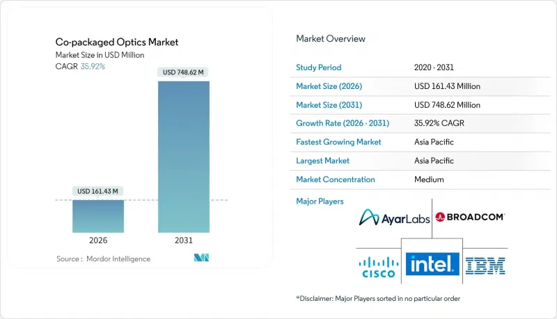
預計到 2025 年,共封裝光學元件 (CPO) 市值將達到 1.2 億美元,從 2026 年的 1.6 億美元成長到 2031 年的 7.5 億美元。
預計在預測期(2026-2031 年)內,複合年成長率將達到 35.92%。
矽光電整合技術最初主要處於實驗階段,如今受益於半導體製造的大規模生產和先進的封裝技術,使超大規模營運商能夠在降低電力消耗的同時,實現與 51.2 Tbps交換器矽晶相當的頻寬密度。其成長動力源自於三大互補趨勢:(1) 人工智慧訓練叢集需要比傳統雲端架構更高的東西向頻寬;(2) 北美和歐盟的能源效率法規優先考慮降低每Gigabit瓦功耗的解決方案;(3) 代工廠的普及(尤其是台積電的矽光電封裝專案)降低了每條光通道的成本並產量比率了良率。由於光元件供應商、半導體製造商和新興的矽光電專家都在競相解決供應阻礙因素的異質整合難題,市場競爭仍然激烈。隨著開放運算社群不斷完善介面規範,共封裝光元件市場可望從早期採用者階段過渡到主流資料中心基礎架構階段。
全球共封裝光學元件 (CPO) 市場趨勢與洞察
51.2T交換器矽晶的量產需要1.6T CPO
博通的Bailly平台證明,在其Tomahawk 5交換器中整合八個6.4Tbps光引擎,與可插拔收發器相比,功耗降低了70%。由於傳統電纜無法維持51.2Tbps ASIC所需的訊號完整性,超大規模營運商被迫重新評估其網路拓撲結構。 800G可插拔設備的機架級散熱設計預算已接近實際極限,這加劇了經濟差距,並促使採購部門將共封裝光模組(CPO)視為必備技術,而非實驗性計劃。隨著第三代200Gbit/s通道的CPO進入量產階段,共封裝光模組市場如今擁有了清晰的技術藍圖,與2026-2028年的交換器矽晶更新周期相契合。這使得設備OEM廠商能夠加快設計採用速度,並確保中期需求的可預測性。
超大規模資料中心的節能要求
隨著各大雲端服務供應商宣布淨零排放承諾,每Gigabit的電力消耗量指標日益受到關注。日月光(ASE)展示的低於5pJ/bit的光引擎證實,將光模組整合到交換器封裝內可以降低DSP功耗並消除銅互連損耗。從歐盟碳定價機製到城市層級暫停新建資料中心,監管壓力使得降低功耗成為基板挑戰。業者提出與節能相關的三年投資回收期目標,同時推廣採用共封裝光學模組,以此在不超出站點電力預算的情況下提高機架密度。這種政策環境正在將技術優勢轉化為投資動力,並透過長期採購協議推動需求成長。
製造複雜性和異質整合帶來回報
共封裝光學元件 (CPO) 將矽光電、III-V族雷射和先進基板整合到毫米級機殼中。在鍵結高功率晶粒的同時,以數十奈米的精度對準光波導會在多個製程步驟中引入損耗。 NVIDIA 先進的 CoWoS 生產線在 Blackwell 量產爬坡階段的產量比率下降凸顯了此製程視窗的脆弱性。材料不匹配導致的熱應力需要特殊的界面層和主動冷卻,從而增加了元件數量和檢測步驟。在技術成熟之前,批量供應將受到限制,這將延長二級 OEM 廠商的前置作業時間,並抑制共封裝光學元件市場近期的出貨量預測。
細分市場分析
到2025年,3.2 Tbps光模組將佔共封裝光模組市場收入的37.92%,這反映了Tomahawk 4級交換器的裝置量。然而,隨著人工智慧叢集對更高速率光纖網路的需求不斷成長,6.4 Tbps及更高速率的設備到2031年將以58.64%的複合年成長率成長。將單一6.4 Tbps引擎與51.2 Tbps ASIC晶片整合,可實現8條200 Gbit/s的光通道。這不僅將交換器到模組的功耗預算減半,還省去了重定時器級。廠商已製定了6.4 Tbps及更高速率藍圖,以配合2026年及以後的伺服器更新周期。
展望未來,晶圓代工廠的藍圖預測,12.8 Tbps 的引擎將在單一封裝內堆疊多個光核心,其中最高頻寬預計將超過所有其他資料速率等級。雖然低於 1.6 Tbps 的共封裝光模組 (CPO) 仍然適用於成本優先於密度的邊緣設備,但超大規模競標檔案現在已將 200G/通道的訊號路徑指定為標準。隨著這一轉變的推進,預計到 2029 年,用於 6.4 Tbps 及更高速率設備的共封裝光模組的市場價值將超過所有低速率光模組市場價值的總和。
到2025年,光學引擎將佔總收入的41.12%,而隨著廠商掌握片上發光技術,雷射光源的複合年成長率將達到43.71%。採用中國產200mm矽晶圓製造的整合式磷化銦雷射陣列無需外部泵浦雷射器,並降低了封裝高度,從而降低了材料成本並提高了可靠性。
由於控制器功能整合在封裝內,電子積體電路的需求保持穩定,但其附加價值來源正轉向雷射技術創新。整合光源無需光纖尾纖,使系統設計人員能夠實現更薄的機架頂部交換機,從而釋放前面板空間。因此,在超超大規模資料中心業者和雷射代工廠之間簽訂的多年供應協議的支持下,用於雷射元件的共封裝光學元件的市場規模正從利基市場轉向核心市場。
共封裝光學元件 (CPO) 市場按資料速率(<1.6T、1.6T、3.2T 以上)、元件(光引擎、電子 IC、雷射源、連接器、封裝等)、整合方法(板載光學元件、共封裝光學元件)、最終用途(超大規模資料中心業者、資料中心、整合方法(板載光學元件、共封裝光學元件)、最終用途(美國通訊業者和歐洲地區運營商、北美地區、其他地區)。
區域分析
亞太地區預計到2025年將佔全球營收的32.78%,年複合成長率達41.99%,主要得益於政府補貼和垂直整合的供應鏈。中國82億元人民幣(約1300億日元)的補貼推動了8英寸矽光子光電的生產和雷射整合,從而降低了元裝置成本。日本經濟產業省已撥款3.05億美元給NTT、英特爾和SK海力士,用於共同開發光晶片,從而加強日本國內的設計生態系統。韓國正透過調整其高頻寬藍圖,使其與光介面技術相契合,從而對這項合作做出補充。
北美透過超大規模營運商滿足了大部分終端用戶需求。博通、英特爾和英偉達是該地區技術基礎的支柱,而台積電位於亞利桑那州的晶圓廠則引入了本土封裝能力,從而縮短了美國雲端客戶的前置作業時間。因此,共封裝光學元件市場受益於晶片設計與內部消費相結合的閉合迴路,即使生產日益分散於全球各地,也鞏固了該地區的市場佔有率。
互通性和永續性是歐洲的優先事項。總部位於歐盟的開放運算專案(OCP)負責開發介面設計並制定全球部署實務。碳定價立法進一步推動了部署,營運商透過將可插拔光學模組轉向共封裝裝置,實現了30%至50%的節能。併購活動,例如諾基亞以23億美元收購Infinera,顯示該地區有意確保自身光纖通訊智慧財產權並提升價值鏈地位。
其他福利:
- Excel格式的市場預測(ME)表
- 3個月的分析師支持
目錄
第1章 引言
- 研究假設和市場定義
- 調查範圍
第2章調查方法
第3章執行摘要
第4章 市場情勢
- 市場概覽
- 市場促進因素
- 51.2 T交換器矽晶大規模生產(需 1.6 T CPO)
- 超大規模資料中心能源效率強制性要求
- AI/ML叢集頻寬需求激增
- 800G/1.6T 可插拔過渡件達到熱極限
- 透過代工廠參與實現大規模生產的經濟效益(例如,台積電 COUPE 專案)
- 透過開放式運算主導的首席產品長 (CPO) 協作減少供應商鎖定
- 市場限制
- 製造複雜性與異質整合產量比率
- 互通性和標準的不成熟
- 光學模組所有權轉移至交換器ASIC供應商
- 光子封裝技能差距
- 價值鏈分析
- 監管環境
- 技術展望
- 宏觀經濟因素的影響
- 對延遲敏感型流量的影響
- 波特五力分析
- 新進入者的威脅
- 買方的議價能力
- 供應商的議價能力
- 替代品的威脅
- 競爭對手之間的競爭
- 投資與資金籌措分析
第5章 市場規模與成長預測
- 按數據速率
- 小於1.6噸
- 1.6 T
- 3.2 T
- 6.4噸或以上
- 按組件
- 輕型引擎
- 積體電路
- 雷射光源
- 連接器和包裝
- 其他
- 透過整合方法
- 機載光學設備
- 共封裝光學元件
- 按最終用途
- 超大規模雲端資料中心
- 企業資料中心
- 通訊業者中心局
- 高效能運算和人工智慧/機器學習叢集
- 其他
- 按地區
- 北美洲
- 美國
- 加拿大
- 南美洲
- 巴西
- 其他南美洲
- 歐洲
- 德國
- 英國
- 法國
- 荷蘭
- 其他歐洲地區
- 亞太地區
- 中國
- 日本
- 韓國
- 印度
- 亞太其他地區
- 中東和非洲
- 中東
- 以色列
- 土耳其
- GCC
- 其他中東地區
- 非洲
- 南非
- 其他非洲地區
- 中東
- 北美洲
第6章 競爭情勢
- 市場集中度
- 策略趨勢
- 市佔率分析
- 公司簡介
- Ayar Labs Inc.
- Broadcom Inc.
- Cisco Systems Inc.
- IBM Corporation
- Intel Corporation
- Ranovus Inc.
- TE Connectivity Ltd.
- Furukawa Electric Co., Ltd.
- Hisense Broadband Multimedia Technology Co., Ltd.
- POET Technologies Inc.
- Kyocera Corporation
- HiSilicon(Huawei Technologies Co., Ltd.)
- SENKO Advanced Components, Inc.
- Sumitomo Electric Industries, Ltd.
- Coherent Corp.
- Taiwan Semiconductor Manufacturing Company Limited(TSMC)
- Lumentum Holdings Inc.
- NVIDIA Corporation
- Marvell Technology, Inc.
- Ciena Corporation
- Nokia Corporation
- InnoLight Technology(Suzhou)Ltd.
- Acacia Communications Inc.
- Hon Hai Precision Industry Co., Ltd.(Foxconn)
- Jabil Inc.
第7章 市場機會與未來展望
The co-packaged optics market was valued at USD 0.12 billion in 2025 and estimated to grow from USD 0.16 billion in 2026 to reach USD 0.75 billion by 2031, at a CAGR of 35.92% during the forecast period (2026-2031).
Silicon photonics integration, once largely experimental, now benefits from high-volume semiconductor manufacturing and advanced packaging, enabling hyperscale operators to pursue bandwidth densities that match 51.2 Tbps switch silicon while lowering power budgets. Growth momentum stems from three reinforcing trends: (1) AI training clusters require far denser east-west bandwidth than classic cloud architectures, (2) energy-efficiency mandates in North America and the EU prioritize solutions that trim watt-per-gigabit metrics, and (3) foundry participation-most visibly TSMC's silicon-photonics packaging programs-reduces cost per optical lane and improves yield. Competitive intensity remains high as optical component vendors, semiconductor houses, and new silicon-photonics specialists race to solve heterogeneous-integration challenges that still constrain supply. As open compute communities refine interface specifications, the co-packaged optics market is positioned to shift from early adopter status to mainstream data-center infrastructure.
Global Co-packaged Optics Market Trends and Insights
Ramp-up of 51.2T switch silicon requiring 1.6T CPO
Broadcom's Bailly platform showed how embedding eight 6.4 Tbps optical engines beside a Tomahawk 5 switch delivered 70% lower power draw than pluggable transceivers. Hyperscale operators consequently reassessed network topologies because legacy electrical traces could not sustain the signal integrity demanded by 51.2 Tbps ASICs. The economic gap widened when rack-level thermal budgets for 800G pluggables hit practical ceilings, prompting procurement teams to treat co-packaged optics as a necessity rather than a lab project. As the third-generation CPO with 200 Gbit/s lanes enters production, the co-packaged optics market gains a clear technical roadmap that aligns with 2026-2028 switch-silicon refresh cycles. Equipment OEMs, therefore, accelerate design wins, locking in demand visibility over the medium term.
Hyperscale data-center energy-efficiency mandates
Net-zero pledges published by major cloud providers intensified scrutiny on watts-per-gigabit metrics. ASE's demonstration of <5 pJ/bit optical engines confirmed that integrating optics inside the switch package cuts DSP power and eliminates copper trace losses. Regulatory pressure-from carbon-pricing schemes in the EU to city-level moratoriums on new data-center builds-made the power reduction a board-level issue. Operators outlined three-year payback targets tied to energy savings and, in parallel, positioned co-packaged optics as a lever to unlock higher rack densities without breaching site power envelopes. The policy environment, therefore, transforms a technical benefit into an investment imperative, boosting demand through long-term purchase agreements.
Manufacturing complexity and heterogeneous integration yield
Co-packaged optics combines silicon photonics, III-V lasers, and advanced substrates inside a millimeter-scale envelope. Aligning optical waveguides to within tens of nanometers while also attaching high-power switch dice drives yields loss across multiple process steps. Recent yield slippages in advanced CoWoS lines, highlighted during NVIDIA's Blackwell ramp, underscore the fragile process window. Material-mismatch thermal stress necessitates exotic interface layers and active cooling, increasing part counts and inspection steps. Until learning curves mature, volume availability remains constrained, elongating lead times for tier-two OEMs and tempering near-term shipment forecasts for the co-packaged optics market.
Other drivers and restraints analyzed in the detailed report include:
- Surge in AI/ML cluster bandwidth demand
- Foundry participation enabling volume economics
- Interoperability and standards immaturity
For complete list of drivers and restraints, kindly check the Table Of Contents.
Segment Analysis
The 3.2 Tbps segment accounted for 37.92% of the co-packaged optics market revenue in 2025, reflecting the installed base of Tomahawk 4 class switches. However, >=6.4 Tbps devices are posting a 58.64% CAGR through 2031 as AI clusters press for higher radix fabrics. A single 6.4 Tbps engine co-located with a 51.2 Tbps ASIC yields eight optical lanes at 200 Gbit/s each, which halves the switch-to-module power budget and eliminates retimer stages. Vendors thus lock the >=6.4 Tbps roadmap into server refresh cycles beginning in 2026.
Looking forward, the foundry roadmaps project 12.8 Tbps engines that stack multiple optical cores within one package, positioning the top-end band to outgrow all other data-rate tiers. While sub-1.6 Tbps CPO remains viable for edge appliances where cost outranks density, hyperscale bidding documents now stipulate 200G/lane signal paths as a baseline. As this migration unfolds, the co-packaged optics market size for >=6.4 Tbps devices is set to outstrip the combined value of lower speed classes by 2029.
Optical engines represented 41.12% of 2025 revenue, yet laser sources are expanding at a 43.71% CAGR as vendors master on-chip light generation. China's integrated indium-phosphide laser arrays, produced on 200 mm silicon wafers, removed the need for external pump lasers and reduced package height, trimming material cost, and improved reliability.
Electronics ICs maintain steady demand as controller functions migrate on-package, but the incremental value pool is shifting toward laser innovation. With integrated sources eliminating fiber pigtails, system architects design slimmer top-of-rack switches and free front-panel real estate. The co-packaged optics market size for laser devices is therefore moving from niche to core, supported by multi-year supply agreements between hyperscalers and laser foundries.
Co-Packaged Optics Market is Segmented by Data Rate (< 1. 6T, 1. 6T, 3. 2T, and Above), Component (Optical Engine, Electrical IC, Laser Source, Connector and Packaging, and More), Integration Approach (On-Board Optics, and Co-Packaged Optics), End-Use Application (Hyperscale Cloud Data Centers, Enterprise Data Centers, and More), and Geography (North America, South America, Europe, Asia-Pacific, and Middle East and Africa).
Geography Analysis
Asia-Pacific commanded 32.78% of 2025 revenue and is advancing at a 41.99% CAGR, powered by government subsidies and vertically integrated supply. China's CNY 8.2 billion subsidy enabled eight-inch silicon-photonics wafer production and laser integration that compresses the bill-of-materials cost. Japan's Ministry of Economy, Trade and Industry funded USD 305 million for NTT, Intel, and SK Hynix to co-develop optical chips, strengthening local design ecosystems. South Korea complements the loop by aligning high-bandwidth memory roadmaps with optical interfaces.
North America supplies the bulk of end-user demand through hyperscale operators. Broadcom, Intel, and NVIDIA anchor the regional technology stack, while TSMC's Arizona fabs introduce domestic packaging capacity that shortens lead times for US cloud customers. The co-packaged optics market, therefore, benefits from a closed loop that links chip design to captive consumption, reinforcing the region's share even as production diversifies globally.
Europe prioritizes interoperability and sustainability. Open Compute Project chapters headquartered in the EU draft interface blueprints, shaping global deployment practices. Carbon-pricing legislation further propels adoption; operators document 30-50% power savings when shifting from pluggable optics to co-packaged lanes. M&A activity, typified by Nokia's USD 2.3 billion acquisition of Infinera, signals the region's intent to secure proprietary optical IP and climb the value chain.
- Ayar Labs Inc.
- Broadcom Inc.
- Cisco Systems Inc.
- IBM Corporation
- Intel Corporation
- Ranovus Inc.
- TE Connectivity Ltd.
- Furukawa Electric Co., Ltd.
- Hisense Broadband Multimedia Technology Co., Ltd.
- POET Technologies Inc.
- Kyocera Corporation
- HiSilicon (Huawei Technologies Co., Ltd.)
- SENKO Advanced Components, Inc.
- Sumitomo Electric Industries, Ltd.
- Coherent Corp.
- Taiwan Semiconductor Manufacturing Company Limited (TSMC)
- Lumentum Holdings Inc.
- NVIDIA Corporation
- Marvell Technology, Inc.
- Ciena Corporation
- Nokia Corporation
- InnoLight Technology (Suzhou) Ltd.
- Acacia Communications Inc.
- Hon Hai Precision Industry Co., Ltd. (Foxconn)
- Jabil Inc.
Additional Benefits:
- The market estimate (ME) sheet in Excel format
- 3 months of analyst support
TABLE OF CONTENTS
1 INTRODUCTION
- 1.1 Study Assumptions and Market Definition
- 1.2 Scope of the Study
2 RESEARCH METHODOLOGY
3 EXECUTIVE SUMMARY
4 MARKET LANDSCAPE
- 4.1 Market Overview
- 4.2 Market Drivers
- 4.2.1 Ramp-up of 51.2 T switch silicon requiring 1.6 T CPO
- 4.2.2 Hyperscale data-center energy-efficiency mandates
- 4.2.3 Surge in AI/ML cluster bandwidth demand
- 4.2.4 Transition to 800 G/1.6 T pluggables hitting thermal limits
- 4.2.5 Foundry participation (e.g., TSMC COUPE) enabling volume economics
- 4.2.6 Open Compute-driven CPO collaboration reducing vendor lock-in
- 4.3 Market Restraints
- 4.3.1 Manufacturing complexity and heterogeneous-integration yield
- 4.3.2 Interoperability and standards immaturity
- 4.3.3 Shift of optical-module ownership to switch-ASIC vendors
- 4.3.4 Photonic-packaging workforce skills gap
- 4.4 Value Chain Analysis
- 4.5 Regulatory Landscape
- 4.6 Technological Outlook
- 4.7 Impact of Macroeconomic Factors
- 4.8 Latency-Sensitive Traffic Impact
- 4.9 Porter's Five Forces Analysis
- 4.9.1 Threat of New Entrants
- 4.9.2 Bargaining Power of Buyers
- 4.9.3 Bargaining Power of Suppliers
- 4.9.4 Threat of Substitutes
- 4.9.5 Intensity of Competitive Rivalry
- 4.10 Investment and Funding Analysis
5 MARKET SIZE AND GROWTH FORECASTS (VALUE)
- 5.1 By Data Rate
- 5.1.1 < 1.6 T
- 5.1.2 1.6 T
- 5.1.3 3.2 T
- 5.1.4 6.4 T and Above
- 5.2 By Component
- 5.2.1 Optical Engine
- 5.2.2 Electrical IC
- 5.2.3 Laser Source
- 5.2.4 Connector and Packaging
- 5.2.5 Others
- 5.3 By Integration Approach
- 5.3.1 On-board Optics
- 5.3.2 Co-packaged Optics
- 5.4 By End-use Application
- 5.4.1 Hyperscale Cloud Data Centers
- 5.4.2 Enterprise Data Centers
- 5.4.3 Telco Central Offices
- 5.4.4 HPC and AI/ML Clusters
- 5.4.5 Others
- 5.5 By Geography
- 5.5.1 North America
- 5.5.1.1 United States
- 5.5.1.2 Canada
- 5.5.2 South America
- 5.5.2.1 Brazil
- 5.5.2.2 Rest of South America
- 5.5.3 Europe
- 5.5.3.1 Germany
- 5.5.3.2 United Kingdom
- 5.5.3.3 France
- 5.5.3.4 Netherlands
- 5.5.3.5 Rest of Europe
- 5.5.4 Asia-Pacific
- 5.5.4.1 China
- 5.5.4.2 Japan
- 5.5.4.3 South Korea
- 5.5.4.4 India
- 5.5.4.5 Rest of Asia-Pacific
- 5.5.5 Middle East and Africa
- 5.5.5.1 Middle East
- 5.5.5.1.1 Israel
- 5.5.5.1.2 Turkey
- 5.5.5.1.3 GCC
- 5.5.5.1.4 Rest of Middle East
- 5.5.5.2 Africa
- 5.5.5.2.1 South Africa
- 5.5.5.2.2 Rest of Africa
- 5.5.5.1 Middle East
- 5.5.1 North America
6 COMPETITIVE LANDSCAPE
- 6.1 Market Concentration
- 6.2 Strategic Moves
- 6.3 Market Share Analysis
- 6.4 Company Profiles (includes Global level Overview, Market level overview, Core Segments, Financials, Strategic Information, Market Rank/Share, Products and Services, Recent Developments)
- 6.4.1 Ayar Labs Inc.
- 6.4.2 Broadcom Inc.
- 6.4.3 Cisco Systems Inc.
- 6.4.4 IBM Corporation
- 6.4.5 Intel Corporation
- 6.4.6 Ranovus Inc.
- 6.4.7 TE Connectivity Ltd.
- 6.4.8 Furukawa Electric Co., Ltd.
- 6.4.9 Hisense Broadband Multimedia Technology Co., Ltd.
- 6.4.10 POET Technologies Inc.
- 6.4.11 Kyocera Corporation
- 6.4.12 HiSilicon (Huawei Technologies Co., Ltd.)
- 6.4.13 SENKO Advanced Components, Inc.
- 6.4.14 Sumitomo Electric Industries, Ltd.
- 6.4.15 Coherent Corp.
- 6.4.16 Taiwan Semiconductor Manufacturing Company Limited (TSMC)
- 6.4.17 Lumentum Holdings Inc.
- 6.4.18 NVIDIA Corporation
- 6.4.19 Marvell Technology, Inc.
- 6.4.20 Ciena Corporation
- 6.4.21 Nokia Corporation
- 6.4.22 InnoLight Technology (Suzhou) Ltd.
- 6.4.23 Acacia Communications Inc.
- 6.4.24 Hon Hai Precision Industry Co., Ltd. (Foxconn)
- 6.4.25 Jabil Inc.
7 MARKET OPPORTUNITIES AND FUTURE OUTLOOK
- 7.1 White-space and Unmet-need Assessment
 共封裝光學元件市場預測至2034年-按組件、技術、資料傳輸速率、封裝類型、應用、最終使用者和地區分類的全球分析
 共封裝光元件市場:按組件、資料速率、整合類型和最終用戶分類-市場規模、產業動態、機會分析和預測(2026-2035 年)
 全球共同封裝光學市場(2027-2037 年)全球共封裝光學元件市場規模、佔有率、趨勢及成長分析報告(2026-2034)
 共封裝光學元件市場:依組件、材料、資料傳輸速率、外形規格及應用分類-2026-2032年全球市場預測
 全球共封裝光元件(CPO)模組市場洞察及預測(至2033年)
 CPO試驗中的創新:共封裝光學模組檢驗的市場機會
 共封裝光元件 (CPO) 在人工智慧資料中心的應用:十年市場與技術預測
 共封裝光元件市場規模、佔有率及成長分析(按組件、資料速率、應用和地區分類)-2026-2033年產業預測
 共封裝光模組(CPO)-全球市場佔有率和排名、總收入和需求預測(2025-2031年)