


 |
市場調查報告書
商品編碼
1851742
半導體材料:市場佔有率分析、行業趨勢、統計數據和成長預測(2025-2030 年)Semiconductor Materials - Market Share Analysis, Industry Trends & Statistics, Growth Forecasts (2025 - 2030) |
||||||
※ 本網頁內容可能與最新版本有所差異。詳細情況請與我們聯繫。
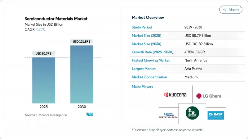
預計到 2025 年,半導體材料市場規模將達到 807.9 億美元,到 2030 年將擴大到 1,018.9 億美元,預測期內複合年成長率為 4.75%。
人工智慧最佳化架構的持續發展和車輛電氣化正將傳統矽材料推向物理極限,並重塑材料需求。隨著晶片設計和3D堆疊架構對互連和散熱解決方案的需求日益成長,先進封裝材料正以11.8%的複合年成長率加速成長。儘管製造材料仍佔據主導地位,預計到2024年將佔收入佔有率的63%,但價值創造正在向下游轉移,封裝創新正在影響系統性能。電動車對寬能能隙功率元件的需求成長,以及北美和歐洲國內材料供應鏈因戰略性回流計畫而獎勵,也推動了需求成長。圍繞關鍵化學品的地緣政治緊張局勢(最顯著的例子是日本在2019年對氟化氫的限制)凸顯了多元化籌資策略的重要性。
全球半導體材料市場趨勢與洞察
數位化主導的晶圓廠擴張
到2027年,300毫米晶圓廠產能計畫投資4,000億美元,將是半導體史上規模最大的產能擴張。光是德克薩斯一家就在美國七座晶圓廠投資600億美元,而美光科技計畫在國內記憶體工廠投資2,000億美元。先進晶圓廠每片晶圓消費量的特種化學品比上一代晶圓廠多40%,迫使供應商在多個地區擴大超高純度化學品的生產。
5G/AI終端設備的普及
人工智慧加速器推動了前所未有的頻寬和散熱極限,導致每個封裝晶片的材料成本是傳統處理器的三倍。 HBM堆疊結構依賴矽通孔銅柱和超薄晶片黏接膜,需要富含銀的配方。FUJIFILM的目標是到2030年實現5,000億日圓的半導體材料銷售額,主要驅動力是專為人工智慧節點量身打造的EUV光阻劑。在汽車領域,LG化學用於SiC功率模組的高性能銀膠表明,人工智慧主導的移動性將如何提高對溫度和電壓的要求。
消費性電子產品的循環經濟
預計半導體封裝材料市場在2023年將下滑15.5%,隨後在2024年復甦,顯示智慧型手機和個人電腦市場的放緩將迅速波及化學品需求。高達30%的季度庫存波動將給專注於大批量消費品的供應商帶來壓力。多元化發展至汽車、工業和基礎設施領域可以緩解但無法消除這種波動。人工智慧增強型消費設備的出現可能會降低週期性波動幅度,但同時也帶來新的預測複雜性,因為材料成本上漲將取代銷售成長成為主要的收入促進因素。
細分市場分析
晶圓製造材料,由於每片晶圓需要數百道蝕刻、沉積和平坦化工序,預計到2024年將佔半導體材料市場收入的63%。濕式化學品、電子氣體和化學機械拋光(CMP)耗材是最大的成本組成部分。以以金額為準,到2024年,這部分半導體材料市場的價值將超過500億美元。先進封裝目前規模較小,但隨著晶片分離技術的進步,金屬化密度和熱界面性能將超越有機層壓材料的能力,其市場將以9.2%的複合年成長率成長。因此,半導體材料市場正朝著晶粒晶片架構設計的基板、底部填充材料和模塑化合物方向發展,而封裝原料市場也將以11.8%的複合年成長率成長。
這一轉變也重塑了產業格局。製造供應商將享受規模經濟效益,但成長曲線將更加平緩。例如,基於BT樹脂的基板能夠實現比傳統FR-4更精細的線條和間距,從而提升AI加速器的性能。材料供應商,無論採用何種製程節點和封裝架構,都能透過在晶圓製造初期和模組最終階段分別控制成本,從而獲得跨週期的競爭力。
由於濕式製程化學品在清洗、剝離和蝕刻等製程中發揮普遍作用,它們仍將是最大的材料類別,預計到2024年將佔總支出的24%。隨著製程節點的推進,化學品用量也在增加,最先進的晶圓廠每片晶圓所使用的酸和鹼比28nm製程線多40%。包括氟化氫和三氟化氮在內的特種氣體面臨地緣政治供應限制。日本2019年的出口限制導致韓國的氟化氫出貨量減少了96.8%,促使韓國轉向台灣、比利時和美國地採購。
隨著製程尺寸的不斷縮小,平坦化步驟也隨之增加,CMP 漿料和墊片的需求量穩定上升。光阻劑隨著 EUV 技術的普及而不斷發展,新型聚合物平台必須能夠承受 13.5nm 的光子曝光,同時劣化線邊緣粗糙度。基板技術的創新也從 300mm 矽擴展到用於功率元件的高品質 SiC 晶錠和 200mm GaN 晶圓。總而言之,這些變化正在再形成半導體材料市場,迫使供應商在純度、永續性和成本之間尋求平衡。
半導體材料市場按應用(製造、封裝)、材料類型(晶圓基板、特殊材料、其他)、終端用戶產業(消費電子、通訊、其他)、技術節點、晶圓廠所有權(整合元件製造商、純晶圓廠、其他)和地區進行細分。市場預測以美元計價。
區域分析
亞太地區預計到2024年將佔全球銷售額的55%,主要得益於台灣、韓國、日本和中國當地密集的製造業生態系統。然而,這種區域集中也使得供應鏈更容易受到出口管制衝擊,2019年的氫氟酸事件就印證了這一點。日本供應商正透過投資5.45億美元新創工廠和進行收購來增強自身抵禦風險的能力,以確保對高純度生產線的本地化控制。
北美是成長最快的地區,在《晶片法案》(CHIPS Act)520億美元激勵措施的推動下,預計到2030年將實現6.4%的複合年成長率。英特爾、台積電和三星正在建造年產能超過2,000萬片的晶圓,這得益於液化空氣集團(在愛達荷州投資2.5億美元)和恩特格里斯(在科羅拉多斯普林斯投資7,500萬美元)的同步投資。國內封裝和測試的擴張正在縮短前置作業時間,並刺激對本地生產的焊球合金和先進基板的需求。同時,環境監管機構正在加速推廣無PFAS化學品,這為本地創新者提供了立足之地。
歐洲正利用晶片製造程序,力爭2030年佔據全球20%的市場。默克、BASF和林德正在升級其超純硫酸和氨生產線,以支援德國和法國的新工廠。印度正崛起為成熟的節點和輔助OSAT(外包半導體加工)中心,吸引特種氣體生產商進行待開發區投資。中東和非洲仍在發展中,但預計將受益於各國為可再生能源計劃相關的電力設備組裝採取的本土化措施。總而言之,這些措施將從地理上重新分配半導體材料市場,在降低地緣政治風險的同時,透過冗餘增加總支出。
其他福利:
- Excel格式的市場預測(ME)表
- 3個月的分析師支持
目錄
第1章 引言
- 研究假設和市場定義
- 調查範圍
第2章調查方法
第3章執行摘要
第4章 市場情勢
- 市場概覽
- 市場促進因素
- 數位化主導的工廠擴張
- 5G/AI終端設備的普及
- 汽車電氣化和高級駕駛輔助系統
- 先進節點投資(5nm)
- 晶片組和異構整合物料清單提升
- 區域化主導的安全庫存政策
- 市場限制
- 消費性電子產品的循環經濟
- 新化學品的高資本密集度
- 關於 PFAS 化學品的環境法規
- 亞太地區氫氟酸供應安全
- 價值/供應鏈分析
- 監管環境
- 技術展望
- 波特五力模型
- 供應商的議價能力
- 消費者議價能力
- 新進入者的威脅
- 替代品的威脅
- 競爭對手之間的競爭
第5章 市場規模與成長預測
- 透過使用
- 製造
- 製程化學品
- 光掩模
- 電子氣體
- 光阻劑輔助設備
- 濺鍍靶
- 矽
- 其他加工材料
- 包裝
- 基板
- 導線架
- 陶瓷包裝
- 連接線
- 封裝樹脂
- 晶粒黏接材料
- 其他包裝材料
- 製造
- 依材料類型
- 晶圓基板
- 特種氣體
- 濕式化學品
- 光阻劑和配件
- CMP漿料和墊片
- 先進包裝材料
- 按最終用戶行業分類
- 消費性電子產品
- 通訊領域
- 製造/工業IoT
- 車
- 能源與公用事業
- 其他
- 依技術節點
- 45奈米或以上
- 28-45 nm
- 14-22 nm
- 7-10 nm
- 小於5奈米
- 由 Fab Ownership 提供
- IDM
- 純粹的選角
- 無晶圓廠(透過代工廠購買材料)
- OSAT/組裝和測試
- 按地區
- 北美洲
- 美國
- 加拿大
- 墨西哥
- 歐洲
- 英國
- 德國
- 法國
- 義大利
- 其他歐洲地區
- 亞太地區
- 中國
- 日本
- 印度
- 韓國
- 亞太其他地區
- 中東
- 以色列
- 沙烏地阿拉伯
- 阿拉伯聯合大公國
- 土耳其
- 其他中東地區
- 非洲
- 南非
- 埃及
- 其他非洲地區
- 南美洲
- 巴西
- 阿根廷
- 其他南美洲
- 北美洲
第6章 競爭情勢
- 市場集中度
- 策略趨勢
- 市佔率分析
- 公司簡介
- DuPont de Nemours, Inc.
- BASF SE
- Showa Denko Materials Co., Ltd.
- Tokyo Ohka Kogyo Co., Ltd.
- Shin-Etsu Chemical Co., Ltd.
- Merck KGaA(EMD Electronics)
- LG Chem Ltd.
- Henkel AG and Co. KGaA
- Indium Corporation
- SUMCO Corporation
- JSR Corporation
- KYOCERA Corporation
- Versum Materials(Merck)
- Caplinq Europe BV
- Nichia Corporation
- International Quantum Epitaxy Plc.
- Sumitomo Chemical Co., Ltd.
- DOW Inc.
- Air Liquide Electronics
- Linde plc Electronics
- SK Materials Co., Ltd.
第7章 市場機會與未來展望
The semiconductor materials market size reached USD 80.79 billion in 2025 and is projected to expand to USD 101.89 billion by 2030, advancing at a 4.75% CAGR during the forecast period.
Continued AI-optimized architectures and automotive electrification are reshaping material requirements as traditional silicon approaches fundamental physics limits. Advanced packaging materials are accelerating at an 11.8% CAGR because chiplet designs and 3D stacking architectures need novel interconnect and thermal solutions. Fabrication materials still dominate with a 63% revenue share in 2024, but value creation is migrating downstream where packaging innovation increasingly shapes system performance. Demand is also buoyed by the pivot to wide-bandgap power devices in electric vehicles and by strategic reshoring programs that incentivize domestic material supply chains in North America and Europe. Geopolitical tensions surrounding critical chemicals-most visibly Japan's 2019 hydrogen-fluoride curbs-have underscored the importance of diversified sourcing strategies.
Global Semiconductor Materials Market Trends and Insights
Digitalization-led Fab Expansions
The USD 400 billion earmarked for 300 mm fab equipment through 2027 represents the largest capacity build-out in semiconductor history. Texas Instruments alone has committed USD 60 billion across seven US fabs, while Micron plans USD 200 billion in domestic memory facilities. . Each advanced fab consumes 40% more specialty chemicals per wafer than the previous generation, intensifying pressure on suppliers to scale ultra-high-purity production in multiple geographies.
5G/AI End-Device Proliferation
AI accelerators push unprecedented bandwidth and thermal envelopes, tripling materials spend per packaged chip relative to conventional processors. HBM stacks rely on through-silicon-via copper pillars and ultra-thin die-attach films that demand silver-rich formulations. Fujifilm has targeted JPY 500 billion in semiconductor-materials revenue by 2030, largely from EUV photoresists tailored for AI-centric nodes. On the automotive side, LG Chem's high-performance silver paste for SiC power modules exemplifies how AI-driven mobility raises both temperature and voltage requirements.
Cyclicality of Consumer Electronics
The semiconductor packaging materials segment fell 15.5% in 2023 before rebounding in 2024, illustrating how smartphone and PC slowdowns ripple quickly through chemical demand. Inventory swings of up to 30% within a quarter pressure suppliers devoted to high-volume consumer lines. Diversification into automotive, industrial and infrastructure is mitigating but not eliminating this volatility. The advent of AI-enhanced consumer devices may lower cyclical amplitude yet introduce fresh forecasting complexity as bill-of-materials inflation replaces unit growth as the primary revenue lever.
Other drivers and restraints analyzed in the detailed report include:
- Automotive Electrification & ADAS
- Advanced-Node Investments (<=5 nm)
- High Capital Intensity for New Chemistries
For complete list of drivers and restraints, kindly check the Table Of Contents.
Segment Analysis
Fabrication materials commanded 63% revenue in 2024, reflecting the hundreds of etch, deposition and planarization steps per wafer. Wet chemicals, electronic gases and CMP consumables form the largest cost pools. In value terms, this slice of the semiconductor materials market size equated to more than USD 50 billion in 2024. Advanced packaging, while smaller today, is scaling at a 9.2% CAGR as chiplet partitioning pushes metallization density and thermal-interface performance beyond organic laminate capabilities. The semiconductor materials market is therefore tilting toward substrates, under-fills and mold compounds engineered for multi-die architectures, supported by an 11.8% CAGR in packaging raw materials.
The pivot also recasts industry power dynamics. Fabrication suppliers benefit from scale but face flatter growth curves, whereas packaging innovators can secure design-in wins with higher long-term elasticity. For instance, BT-resin-based substrates enable finer lines and spaces than traditional FR-4, unlocking performance gains in AI accelerators. Materials vendors that straddle both process nodes and package architectures gain cross-cycle resilience, capturing spend both at wafer start and at module finish.
Wet-process chemicals remained the largest material class, representing 24% of 2024 spend, thanks to their universal role in cleaning, stripping and etching. Ongoing node migration increases dosage intensity-leading-edge fabs use 40% more acids and bases per wafer than 28 nm lines. Specialty gases, including hydrogen fluoride and nitrogen trifluoride, follow closely in value and face geopolitical supply scrutiny. Japan's 2019 export restrictions slashed hydrogen-fluoride shipments to South Korea by 96.8%, prompting rapid dual-sourcing across Taiwan, Belgium and the United States.
CMP slurries and pads show steady upticks as the number of planarization steps rises with each design shrink. Photoresists evolve with EUV adoption; new polymer platforms must endure 13.5 nm photon bombardment without line-edge roughness degradation. Substrate innovation is broadening beyond 300 mm silicon to include high-quality SiC boules and 200 mm GaN wafers for power devices. Collectively, these shifts are reshaping the semiconductor materials market, forcing suppliers to balance purity, sustainability and cost.
Semiconductor Materials Market Segmented by Application (Fabrication, Packaging), Material Type (Wafer Substrates, Specialty and More), End-User Industry (Consumer Electronics, Telecommunications, and More), Technology Node, Fab Ownership (IDM, Pure-Play and More), and Geography. The Market Forecasts are Provided in Terms of Value (USD).
Geography Analysis
Asia-Pacific commanded 55% of 2024 revenue owing to its dense manufacturing ecosystem across Taiwan, South Korea, Japan and mainland China. However, the region's concentration exposes supply chains to export-control shocks as evidenced by the 2019 hydrogen-fluoride episode. Japanese suppliers are fortifying resilience with USD 545 million in new chemical plants and targeted acquisitions to secure local control of high-purity lines.
North America is the fastest-growing territory, advancing at a 6.4% CAGR through 2030 on the back of USD 52 billion in CHIPS Act incentives. Intel, TSMC and Samsung are collectively building more than 20 million wafers per-year of capacity, catalysing parallel investments from Air Liquide (USD 250 million in Idaho) and Entegris (USD 75 million for Colorado Springs). Domestic packaging and test expansions are shortening lead times and stimulating demand for solder-ball alloys and advanced substrates produced within the region. Environmental regulators are simultaneously accelerating adoption of PFAS-free chemistries, giving local innovators a foothold.
Europe is leveraging its Chips Act to reach 20% global share by 2030. Merck, BASF and Linde are upgrading ultra-purity sulfuric and ammonia lines to support new fabs in Germany and France. India is emerging as a secondary hub for mature-node and OSAT work, attracting specialty-gas makers with greenfield investments. The Middle East and Africa remain nascent but could benefit from sovereign efforts to localize power-device assembly tied to renewable energy projects. Collectively these moves are geographically redistributing the semiconductor materials market, increasing total spend through redundancy while easing geopolitical risk.
- DuPont de Nemours, Inc.
- BASF SE
- Showa Denko Materials Co., Ltd.
- Tokyo Ohka Kogyo Co., Ltd.
- Shin-Etsu Chemical Co., Ltd.
- Merck KGaA (EMD Electronics)
- LG Chem Ltd.
- Henkel AG and Co. KGaA
- Indium Corporation
- SUMCO Corporation
- JSR Corporation
- KYOCERA Corporation
- Versum Materials (Merck)
- Caplinq Europe B.V.
- Nichia Corporation
- International Quantum Epitaxy Plc.
- Sumitomo Chemical Co., Ltd.
- DOW Inc.
- Air Liquide Electronics
- Linde plc Electronics
- SK Materials Co., Ltd.
Additional Benefits:
- The market estimate (ME) sheet in Excel format
- 3 months of analyst support
TABLE OF CONTENTS
1 INTRODUCTION
- 1.1 Study Assumptions and Market Definition
- 1.2 Scope of the Study
2 RESEARCH METHODOLOGY
3 EXECUTIVE SUMMARY
4 MARKET LANDSCAPE
- 4.1 Market Overview
- 4.2 Market Drivers
- 4.2.1 Digitalisation-led fab expansions
- 4.2.2 5G/AI end-device proliferation
- 4.2.3 Automotive electrification and ADAS
- 4.2.4 Advanced-node investments (5 nm)
- 4.2.5 Chiplet and heterogenous integration BOM uplift
- 4.2.6 Regionalisation-driven safety-stock policies
- 4.3 Market Restraints
- 4.3.1 Cyclicality of consumer electronics
- 4.3.2 High capital intensity for new chemistries
- 4.3.3 Environmental regulations on PFAS chemistries
- 4.3.4 Hydrogen fluoride supply security in APAC
- 4.4 Value / Supply Chain Analysis
- 4.5 Regulatory Landscape
- 4.6 Technological Outlook
- 4.7 Porter's Five Forces
- 4.7.1 Bargaining Power of Suppliers
- 4.7.2 Bargaining Power of Consumers
- 4.7.3 Threat of New Entrants
- 4.7.4 Threat of Substitutes
- 4.7.5 Intensity of Competitive Rivalry
5 MARKET SIZE AND GROWTH FORECASTS (VALUE)
- 5.1 By Application
- 5.1.1 Fabrication
- 5.1.1.1 Process Chemicals
- 5.1.1.2 Photomasks
- 5.1.1.3 Electronic Gases
- 5.1.1.4 Photoresist Ancillaries
- 5.1.1.5 Sputtering Targets
- 5.1.1.6 Silicon
- 5.1.1.7 Other Fabrication Materials
- 5.1.2 Packaging
- 5.1.2.1 Substrates
- 5.1.2.2 Lead-frames
- 5.1.2.3 Ceramic Packages
- 5.1.2.4 Bonding Wire
- 5.1.2.5 Encapsulation Resins
- 5.1.2.6 Die-Attach Materials
- 5.1.2.7 Other Packaging Materials
- 5.1.1 Fabrication
- 5.2 By Material Type
- 5.2.1 Wafer Substrates
- 5.2.2 Specialty Gases
- 5.2.3 Wet Process Chemicals
- 5.2.4 Photoresists and Ancillaries
- 5.2.5 CMP Slurries and Pads
- 5.2.6 Advanced Packaging Materials
- 5.3 By End-User Industry
- 5.3.1 Consumer Electronics
- 5.3.2 Telecommunications
- 5.3.3 Manufacturing / Industrial IoT
- 5.3.4 Automotive
- 5.3.5 Energy and Utility
- 5.3.6 Others
- 5.4 By Technology Node
- 5.4.1 More than 45 nm
- 5.4.2 28-45 nm
- 5.4.3 14-22 nm
- 5.4.4 7-10 nm
- 5.4.5 Less than 5 nm
- 5.5 By Fab Ownership
- 5.5.1 IDM
- 5.5.2 Pure-play Foundry
- 5.5.3 Fabless (materials purchased via foundry)
- 5.5.4 OSAT / Assembly and Test
- 5.6 By Geography
- 5.6.1 North America
- 5.6.1.1 United States
- 5.6.1.2 Canada
- 5.6.1.3 Mexico
- 5.6.2 Europe
- 5.6.2.1 United Kingdom
- 5.6.2.2 Germany
- 5.6.2.3 France
- 5.6.2.4 Italy
- 5.6.2.5 Rest of Europe
- 5.6.3 Asia-Pacific
- 5.6.3.1 China
- 5.6.3.2 Japan
- 5.6.3.3 India
- 5.6.3.4 South Korea
- 5.6.3.5 Rest of Asia-Pacific
- 5.6.4 Middle East
- 5.6.4.1 Israel
- 5.6.4.2 Saudi Arabia
- 5.6.4.3 United Arab Emirates
- 5.6.4.4 Turkey
- 5.6.4.5 Rest of Middle East
- 5.6.5 Africa
- 5.6.5.1 South Africa
- 5.6.5.2 Egypt
- 5.6.5.3 Rest of Africa
- 5.6.6 South America
- 5.6.6.1 Brazil
- 5.6.6.2 Argentina
- 5.6.6.3 Rest of South America
- 5.6.1 North America
6 COMPETITIVE LANDSCAPE
- 6.1 Market Concentration
- 6.2 Strategic Moves
- 6.3 Market Share Analysis
- 6.4 Company Profiles (includes Global level Overview, Market level overview, Core Segments, Financials as available, Strategic Information, Market Rank/Share for key companies, Products and Services, and Recent Developments)
- 6.4.1 DuPont de Nemours, Inc.
- 6.4.2 BASF SE
- 6.4.3 Showa Denko Materials Co., Ltd.
- 6.4.4 Tokyo Ohka Kogyo Co., Ltd.
- 6.4.5 Shin-Etsu Chemical Co., Ltd.
- 6.4.6 Merck KGaA (EMD Electronics)
- 6.4.7 LG Chem Ltd.
- 6.4.8 Henkel AG and Co. KGaA
- 6.4.9 Indium Corporation
- 6.4.10 SUMCO Corporation
- 6.4.11 JSR Corporation
- 6.4.12 KYOCERA Corporation
- 6.4.13 Versum Materials (Merck)
- 6.4.14 Caplinq Europe B.V.
- 6.4.15 Nichia Corporation
- 6.4.16 International Quantum Epitaxy Plc.
- 6.4.17 Sumitomo Chemical Co., Ltd.
- 6.4.18 DOW Inc.
- 6.4.19 Air Liquide Electronics
- 6.4.20 Linde plc Electronics
- 6.4.21 SK Materials Co., Ltd.
7 MARKET OPPORTUNITIES AND FUTURE OUTLOOK
- 7.1 White-space and Unmet-Need Assessment
 全球半導體陶瓷聚焦環市場報告:競爭分析與區域機會(2026-2032 年)
 半導體材料市場報告:按材料、應用、終端用戶產業和地區分類(2026-2034 年)
 碳化矽基板市場報告:趨勢、預測與競爭分析(至2035年)
 半導體管市場:按材料、應用和最終用途分類-2026-2032年全球市場預測半導體材料市場:材料類型、晶圓尺寸、應用和終端用戶產業分類-2026-2032年全球市場預測
 全球先進鑽石材料與技術市場(2026-2036)
 半導體用鑽石材料市場規模、佔有率及成長分析(依材料類型、形狀、應用、終端用戶產業及地區分類)-2026-2033年產業預測
 5G網路可再生半導體材料市場分析及預測(至2035年):類型、產品類型、服務、技術、組件、應用、製程、最終用戶、模組、安裝類型先進透明半導體市場分析及預測(至2035年):依類型、產品類型、技術、應用、材料類型、裝置、最終使用者、功能及安裝類型分類可回收半導體材料市場分析及預測(至2035年):類型、產品、服務、技術、應用、材料類型、製程、最終用戶、功能、設備