


 |
市場調查報告書
商品編碼
1850971
矽光電:市場佔有率分析、產業趨勢、統計數據和成長預測(2025-2030 年)Silicon Photonics - Market Share Analysis, Industry Trends & Statistics, Growth Forecasts (2025 - 2030) |
||||||
※ 本網頁內容可能與最新版本有所差異。詳細情況請與我們聯繫。
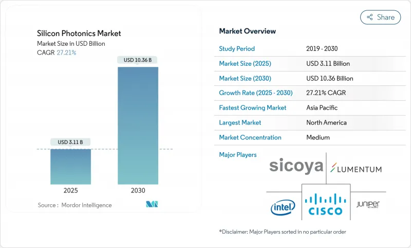
預計到 2025 年,矽光電市場將創造 31.1 億美元的收入,到 2030 年將達到 103.6 億美元,年複合成長率為 27.21%。
隨著超大規模資料中心從 800G 光鏈路升級到 1.6T 光鏈路,汽車 OEM 廠商整合調頻連續波雷射雷達,以及政府獎勵擴大國內半導體產能,市場需求正在加速成長。北美保持領先地位,但亞太地區正透過大規模晶圓廠擴建縮小差距,以滿足 5G、人工智慧和自主供應目標。磷化銦等競爭性材料平台正在推動創新,但也加劇了價格壓力。併購活動凸顯了光子整合日益成長的戰略價值,網路設備供應商、代工廠和雲端服務供應商都在努力確保設計團隊和晶圓生產能力,以應對迫在眉睫的供應限制。
全球矽光電市場趨勢與洞察
在超大規模資料中心採用節能型共封裝光元件
將光引擎直接整合到交換器專用積體電路 (ASIC) 旁邊,可減少電光轉換,並將機架級功耗降低高達 40%。谷歌的光路交換試驗已檢驗延遲有所降低,NVIDIA 和 Marvell 目前都在提供獨特的共封裝模組樣品,這些模組可簡化 AI 叢集的電路板佈局。隨著交換器製造商將光晶片間晶粒標準化,矽光電市場將從中受益,從而推動整合式雷射、調製器和檢測器在 300 毫米晶圓上的封裝量成長。
碳減量指令促進低功耗光連接模組的發展
歐盟資料中心永續性法規旨在大幅降低能耗,要求業者逐步淘汰銅背板。光子鏈路可在保持100Gbps通道傳輸距離的同時,將功耗降低30%。雲端服務供應商宣布了碳中和路線藍圖,並加快了400G和800G矽光電模組的多廠商認證,使其符合企業ESG指標和區域綠色交易。
矽基基板的熱預算限制超過 70°C
研究計畫正在探索具有更高導熱性和對溫度不敏感的共振器設計的不同材料,但這會增加製程步驟和成本,限制了它們在近期內應用於邊緣運算節點。
細分市場分析
隨著超大規模資料中心引入 800G 光模組並完成首批 1.6T 線卡的認證,預計 2024 年光收發器市場收入將成長 62%。矽光電市場正朝著將雷射、調製器和檢測器整合在單一單晶粒上的全端收發器解決方案轉型。市場參與企業正透過模式復用和連續波雷射整合來提高功率效率,從而實現差異化競爭。
晶圓級測試系統正以28.1%的複合年成長率快速成長,主要得益於400G符號/秒以上測試速度對產量比率的嚴格要求。平行光學探針可縮短測試週期,提高吞吐量,進而滿足300毫米生產線的生產能力。供應商正投資於人工智慧輔助缺陷分析,將參數漂移與晶圓廠資料關聯起來,以實現預測性維護。自動化光學測試的廣泛應用將縮短新產品流片的認證時間,並有助於擴大矽光電市場的規模。
到2024年,主動元件將維持58%的市場佔有率,這反映出市場對緊湊型連續波雷射、高消光調變器和低暗電流光電二極體的強勁需求。多工器目前已應用於112 Gbaud PAM4收發器中,並在55°C的封裝溫度下展現出穩定的驅動電壓。晶片製造商改進了異質III-V族雷射的附件,提高了電光轉換效率並降低了外延界面處的光學損耗。
隨著晶圓廠不斷改進低損耗波導管、晶格濾波器和針對 400G ZR+ 調諧的陣列波導管光柵,被動元件的複合年成長率 (CAGR) 最高,達到 29.7%。超低粗糙度蝕刻製程可將插入損耗降低至 0.5dB/cm 以下。採用玻璃波導管的印刷光子電路基板可望實現基板級光學背板,進一步拓展矽光電市場的潛在機會。
區域分析
北美地區在《晶片技術創新法案》(CHIPS Act)津貼和人工智慧大型園區快速部署的推動下,預計將在2024年貢獻38%的收入。奧爾巴尼奈米科技中心(Albany NanoTech)晉升為國家級研究中心,以及來自雲端運算領導企業的私人投資,將打造一個涵蓋設計、封裝和先進測試的國內生態系統。該地區矽光電市場的持續發展,取決於代工廠和設備供應商之間能否無縫協作,以克服晶圓級散熱難題。
亞太地區預計到2030年將以35.1%的複合年成長率實現最快成長,中國、日本和韓國正競相建立自主供應鏈。政府補貼涵蓋製造工具、培訓和計量技術,而5G網路的密集化和本土人工智慧Start-Ups的湧現則確保了市場需求。日本對300毫米GaAs-on-Silicon雷射的投資將推動國內供應商實現出口導向型成長,並增強矽光電市場的全球影響力。
歐洲憑藉歐盟晶片法案提供的數十億歐元資金籌措以及在汽車、工業自動化和光電研究領域強大的產業基礎,繼續保持著強勁的發展勢頭。碳中和資料中心的強制性要求將進一步推動光電的應用。南美以及中東和非洲地區正在為電信和邊緣雲端部署開闢新的立足點,但仍依賴進口晶粒和封裝服務,跨國原始設備製造商(OEM)正尋求透過本地組裝夥伴關係關係來填補這一缺口。
其他福利:
- Excel格式的市場預測(ME)表
- 3個月的分析師支持
目錄
第1章 引言
- 研究假設和市場定義
- 調查範圍
第2章調查方法
第3章執行摘要
第4章 市場情勢
- 市場概覽
- 市場促進因素
- 在超大規模資料中心(北美)採用節能型整合光元件
- 促進低功耗光連接模組的碳減排義務(歐盟)
- 5G去程傳輸/回程傳輸升級推動 400/800G 模組(亞洲)
- 基於FMCW的汽車級3級LiDAR計畫矽光電(中國和歐盟)
- 美國國防部對量子和安全光電的資助
- 政府半導體獎勵計畫推動光子晶圓廠擴張(美國/歐盟/亞洲)
- 市場限制
- 矽基基板熱預算限制超過 70°C
- 缺乏標準化包裝會增加非經常性工程成本。
- 在1.55微米以上的波長範圍內與InP和聚合物光電競爭
- 300毫米光子晶圓代工廠代工產能有限,導致前置作業時間延長
- 產業生態系分析
- 監理展望
- 技術展望
- 波特五力分析
- 供應商的議價能力
- 買方的議價能力
- 新進入者的威脅
- 替代品的威脅
- 競爭對手之間的競爭
第5章 市場規模與成長預測
- 依產品
- 光收發器
- 光開關
- 主動光纜(AOC)
- 矽光電感測器
- 晶圓級測試系統
- 多工器/解多工器
- 衰減器和調製器
- 其他
- 按組件
- 主動元件
- 雷射
- 數據機
- 檢測器
- 被動元件
- 波導
- 篩選
- 耦合器
- 其他
- 主動元件
- 按晶圓尺寸
- 300毫米
- 200毫米
- 150毫米或更小
- 按數據速率
- 100 Gbps 或更低
- 200Gbps
- 400Gbps
- 800Gbps
- 1.6 Tbps 或以上
- 透過使用
- 資料中心和高效能運算
- 通訊
- 汽車和自動駕駛汽車
- AR/VR 和消費性電子產品
- 醫療保健和生命科學
- 國防/航太
- 量子計算
- 其他
- 最終用戶
- 超大規模雲端供應商
- 通訊業者
- 汽車原始設備製造商和一級供應商
- 醫療設備製造商
- 政府和國防機構
- 研究和學術機構
- 按地區
- 北美洲
- 美國
- 加拿大
- 墨西哥
- 歐洲
- 德國
- 英國
- 法國
- 義大利
- 西班牙
- 其他歐洲地區
- 亞太地區
- 中國
- 日本
- 韓國
- 印度
- 東南亞
- 澳洲
- 亞太其他地區
- 南美洲
- 巴西
- 其他南美洲
- 中東和非洲
- 中東
- 阿拉伯聯合大公國
- 沙烏地阿拉伯
- 其他中東地區
- 非洲
- 南非
- 其他非洲地區
- 北美洲
第6章 競爭情勢
- 市場集中度
- 策略趨勢
- 市佔率分析
- 公司簡介
- Intel Corporation
- Cisco Systems Inc.
- Broadcom Inc.
- Lumentum Holdings Inc.
- Juniper Networks Inc.
- GlobalFoundries Inc.
- Sicoya GmbH
- Molex LLC
- Marvell Technology Inc.
- MACOM Technology Solutions
- Coherent Corp.
- Hamamatsu Photonics KK
- Ayar Labs Inc.
- NeoPhotonics Corp.
- IBM Corporation
- Hewlett Packard Enterprise
- II-VI Inc.(now Coherent)
- Rockley Photonics
- Infinera Corporation
- Smart Photonics
- DustPhotonics
- PsiQuantum
- POET Technologies
- Tower Semiconductor
第7章 市場機會與未來展望
The silicon photonics market generates USD 3.11 billion in 2025 and is forecast to advance at a 27.21% CAGR, reaching USD 10.36 billion by 2030.
Demand is accelerating as hyperscale data centers shift from 800 G to 1.6 T optical links, automotive OEMs integrate frequency-modulated continuous-wave LiDAR, and government incentives expand domestic semiconductor capacity. North America retains leadership, yet Asia Pacific is closing the gap through large-scale fab expansions aligned with 5G, AI and sovereign-supply objectives. Competing material platforms such as indium phosphide spur innovation but also intensify price pressure, while thermal-budget ceilings above 70 °C force new cooling architectures. M&A activity underscores the rising strategic value of photonic integration, with network equipment vendors, foundries and cloud providers securing design teams and wafer capacity ahead of looming supply constraints.
Global Silicon Photonics Market Trends and Insights
Energy-efficient Co-Packaged Optics Adoption in Hyperscale Data Centers
Directly embedding optical engines beside switch ASICs trims electrical-optical conversions and cuts rack-level power draw by up to 40%. Google's optical circuit switching trials validate latency gains, and both NVIDIA and Marvell now sample proprietary co-packaged modules that streamline board layouts for AI clusters. The silicon photonics market benefits as switch makers standardize optical die-to-die interfaces, creating a volume pull for integrated lasers, modulators and photodetectors packaged on 300 mm wafers.
Carbon-Reduction Mandates Driving Low-Power Optical Interconnects
EU data-center sustainability rules target significant energy savings, prompting operators to phase out copper backplanes. Photonic links show 30% lower consumption in 100 Gbps channels while maintaining reach. Cloud providers publish carbon-neutral roadmaps, accelerating multi-vendor qualification of 400 G and 800 G silicon photonics modules that align with corporate ESG metrics and local green-deal incentives.
Thermal Budget Limitations in Silicon Substrates Above 70 °C
Optical phase stability drops at elevated junction temperatures, forcing elaborate heat sinks and liquid cooling in tightly packed AI servers.Research programs explore heterogeneous materials with higher thermal conductivity and temperature-insensitive resonator designs, yet these add process steps and cost, tempering near-term adoption in edge compute nodes.
Other drivers and restraints analyzed in the detailed report include:
- 5G Fronthaul/Backhaul Upgrade Fueling 400/800 G Modules
- Automotive Level-3 LiDAR Programs Leveraging FMCW Silicon Photonics
- Lack of Standardized Packaging Elevating NRE Costs
For complete list of drivers and restraints, kindly check the Table Of Contents.
Segment Analysis
Optical transceivers generated 62% revenue in 2024 as hyperscalers deployed 800 G optics and qualified early 1.6 T line-cards.Design wins increasingly bundle integrated drivers and thermal monitors, easing system design and lowering capex per port. The silicon photonics market continues to pivot toward full-stack transceiver solutions that collapse laser, modulator and photodetector in one monolithic die. Market entrants differentiate through modal multiplexing and CW-laser integration that improve power efficiency.
Wafer-level test systems show the fastest expansion at 28.1% CAGR, propelled by tighter yield requirements at 400-G symbols /s and above. Parallel optical probing shrinks cycle time and raises throughput to match 300 mm line capacity. Vendors invest in AI-assisted defect analytics, linking parametric drift to fab data and enabling predictive maintenance. Broader use of automated optical test shortens time-to-qualification for new tape-outs, buttressing scale-up of the silicon photonics market.
Active components maintained a 58% share in 2024, reflecting persistent demand for compact CW lasers, high-extinction modulators and low-dark-current photodiodes. Integrated multiplexers now ship in 112Gbaud PAM4 transceivers, demonstrating stable drive voltages at 55 °C case temperatures. Chip makers refine heterogeneous III-V laser attach, boosting wall-plug efficiency and reducing optical loss across epitaxial interfaces.
Passive components post the highest 29.7% CAGR as fabs iterate low-loss waveguides, lattice filters and arrayed-waveguide gratings tailored for 400G ZR+. Ultralow-roughness etch profiles cut insertion loss below 0.5 dB/cm, essential for co-packaged optics. Printed photonic circuit boards embedding glass waveguides promise board-level optical backplanes, further expanding addressable opportunities for the silicon photonics market.
The Silicon Photonics Market Report is Segmented by Product (Optical Transceivers, Optical Switches, and More), Component (Active, and Passive), Wafer Size (300 Mm, 200 Mm, 150 Mm and Below), Application (Data Centers and High-Performance Computing, Telecommunications, and More), End-User (Hyperscale Cloud Providers, Telecom Operators, and More), and Geography. The Market Forecasts are Provided in Terms of Value (USD).
Geography Analysis
North America generated 38% of 2024 revenue, buoyed by CHIPS Act grants and rapid deployment of AI mega-campuses. Albany NanoTech's elevation to national research hub and private-sector investments from cloud leaders lock in a domestic ecosystem spanning design, packaging and advanced testing. Ongoing evolution of the silicon photonics market in the region hinges on seamless collaboration between foundries and equipment vendors to overcome wafer-level thermal setbacks.
Asia Pacific records the fastest 35.1% CAGR through 2030 as China, Japan and South Korea race to anchor sovereign supply chains. Government subsidies cover fab tools, training and metrology, while 5G densification and local AI start-ups guarantee offtake. Japanese investments in 300 mm GaAs-on-silicon lasers position domestic suppliers for export-oriented growth, reinforcing the global breadth of the silicon photonics market.
Europe sustains momentum through the EU Chips Act's multi-billion-euro financing and a strong industrial base in automotive, industrial automation and research photonics. Carbon-neutral data-center mandates further encourage photonic adoption. South America and the Middle East & Africa open new footholds for telecom and edge-cloud deployments, but still rely on imported dies and packaging services, a gap that multinational OEMs strive to close via localized assembly partnerships.
- Intel Corporation
- Cisco Systems Inc.
- Broadcom Inc.
- Lumentum Holdings Inc.
- Juniper Networks Inc.
- GlobalFoundries Inc.
- Sicoya GmbH
- Molex LLC
- Marvell Technology Inc.
- MACOM Technology Solutions
- Coherent Corp.
- Hamamatsu Photonics K.K.
- Ayar Labs Inc.
- NeoPhotonics Corp.
- IBM Corporation
- Hewlett Packard Enterprise
- II-VI Inc. (now Coherent)
- Rockley Photonics
- Infinera Corporation
- Smart Photonics
- DustPhotonics
- PsiQuantum
- POET Technologies
- Tower Semiconductor
Additional Benefits:
- The market estimate (ME) sheet in Excel format
- 3 months of analyst support
TABLE OF CONTENTS
1 INTRODUCTION
- 1.1 Study Assumptions and Market Definition
- 1.2 Scope of the Study
2 RESEARCH METHODOLOGY
3 EXECUTIVE SUMMARY
4 MARKET LANDSCAPE
- 4.1 Market Overview
- 4.2 Market Drivers
- 4.2.1 Energy-Efficient Co-Packaged Optics Adoption in Hyperscale Data Centers (North America)
- 4.2.2 Carbon-Reduction Mandates Driving Low-Power Optical Interconnects (EU)
- 4.2.3 5G Fronthaul/Backhaul Upgrade Fueling 400/800 G Modules (Asia)
- 4.2.4 Automotive Level-3 LiDAR Programs Leveraging FMCW Silicon Photonics (China and EU)
- 4.2.5 Defense Funding for Quantum and Secure Photonics (United States)
- 4.2.6 Government Semiconductor Incentive Schemes Expanding Photonic Fabs (US/EU/Asia)
- 4.3 Market Restraints
- 4.3.1 Thermal Budget Limitations in Silicon Substrates Above 70 °C
- 4.3.2 Lack of Standardized Packaging Elevating NRE Costs
- 4.3.3 Competition from InP and Polymer Photonics Beyond 1.55 µm
- 4.3.4 Limited 300 mm Photonic Foundry capacity Causing Extended Lead Times
- 4.4 Industry Ecosystem Analysis
- 4.5 Regulatory Outlook
- 4.6 Technological Outlook
- 4.7 Porter's Five Forces Analysis
- 4.7.1 Bargaining Power of Suppliers
- 4.7.2 Bargaining Power of Buyers
- 4.7.3 Threat of New Entrants
- 4.7.4 Threat of Substitutes
- 4.7.5 Intensity of Competitive Rivalry
5 MARKET SIZE AND GROWTH FORECASTS (VALUES)
- 5.1 By Product
- 5.1.1 Optical Transceivers
- 5.1.2 Optical Switches
- 5.1.3 Active Optical Cables (AOCs)
- 5.1.4 Silicon Photonic Sensors
- 5.1.5 Wafer-level Test Systems
- 5.1.6 Multiplexers/De-Multiplexers
- 5.1.7 Attenuators and Modulators
- 5.1.8 Others
- 5.2 By Component
- 5.2.1 Active Components
- 5.2.1.1 Lasers
- 5.2.1.2 Modulators
- 5.2.1.3 Photodetectors
- 5.2.2 Passive Components
- 5.2.2.1 Waveguides
- 5.2.2.2 Filters
- 5.2.2.3 Couplers
- 5.2.2.4 Others
- 5.2.1 Active Components
- 5.3 By Wafer Size
- 5.3.1 300 mm
- 5.3.2 200 mm
- 5.3.3 150 mm and Below
- 5.4 By Data Rate
- 5.4.1 <100 Gbps
- 5.4.2 200 Gbps
- 5.4.3 400 Gbps
- 5.4.4 800 Gbps
- 5.4.5 >1.6 Tbps
- 5.5 By Application
- 5.5.1 Data Centers and High-Performance Computing
- 5.5.2 Telecommunications
- 5.5.3 Automotive and Autonomous Vehicles
- 5.5.4 AR/VR and Consumer Electronics
- 5.5.5 Healthcare and Life Sciences
- 5.5.6 Defense and Aerospace
- 5.5.7 Quantum Computing
- 5.5.8 Others
- 5.6 By End-User
- 5.6.1 Hyperscale Cloud Providers
- 5.6.2 Telecom Operators
- 5.6.3 Automotive OEMs and Tier-1 Suppliers
- 5.6.4 Medical Device Manufacturers
- 5.6.5 Government and Defense Agencies
- 5.6.6 Research and Academic Institutions
- 5.7 By Geography
- 5.7.1 North America
- 5.7.1.1 United States
- 5.7.1.2 Canada
- 5.7.1.3 Mexico
- 5.7.2 Europe
- 5.7.2.1 Germany
- 5.7.2.2 United Kingdom
- 5.7.2.3 France
- 5.7.2.4 Italy
- 5.7.2.5 Spain
- 5.7.2.6 Rest of Europe
- 5.7.3 Asia-Pacific
- 5.7.3.1 China
- 5.7.3.2 Japan
- 5.7.3.3 South Korea
- 5.7.3.4 India
- 5.7.3.5 South East Asia
- 5.7.3.6 Australia
- 5.7.3.7 Rest of Asia-Pacific
- 5.7.4 South America
- 5.7.4.1 Brazil
- 5.7.4.2 Rest of South America
- 5.7.5 Middle East and Africa
- 5.7.5.1 Middle East
- 5.7.5.1.1 United Arab Emirates
- 5.7.5.1.2 Saudi Arabia
- 5.7.5.1.3 Rest of Middle East
- 5.7.5.2 Africa
- 5.7.5.2.1 South Africa
- 5.7.5.2.2 Rest of Africa
- 5.7.1 North America
6 COMPETITIVE LANDSCAPE
- 6.1 Market Concentration
- 6.2 Strategic Moves
- 6.3 Market Share Analysis
- 6.4 Company Profiles (includes Global level Overview, Market level overview, Core Segments, Financials as available, Strategic Information, Market Rank/Share for key companies, Products and Services, and Recent Developments)
- 6.4.1 Intel Corporation
- 6.4.2 Cisco Systems Inc.
- 6.4.3 Broadcom Inc.
- 6.4.4 Lumentum Holdings Inc.
- 6.4.5 Juniper Networks Inc.
- 6.4.6 GlobalFoundries Inc.
- 6.4.7 Sicoya GmbH
- 6.4.8 Molex LLC
- 6.4.9 Marvell Technology Inc.
- 6.4.10 MACOM Technology Solutions
- 6.4.11 Coherent Corp.
- 6.4.12 Hamamatsu Photonics K.K.
- 6.4.13 Ayar Labs Inc.
- 6.4.14 NeoPhotonics Corp.
- 6.4.15 IBM Corporation
- 6.4.16 Hewlett Packard Enterprise
- 6.4.17 II-VI Inc. (now Coherent)
- 6.4.18 Rockley Photonics
- 6.4.19 Infinera Corporation
- 6.4.20 Smart Photonics
- 6.4.21 DustPhotonics
- 6.4.22 PsiQuantum
- 6.4.23 POET Technologies
- 6.4.24 Tower Semiconductor
7 MARKET OPPORTUNITIES AND FUTURE OUTLOOK
- 7.1 White-space and Unmet-Need Assessment
 矽光電市場分析與預測(2034年):類型、產品、服務、技術、組件、應用、材料類型、設備、部署與最終用戶
 矽光電市場按產品類型、組件、波導管和最終用途分類-2025-2032年全球預測
 2025年矽光電全球市場報告
 矽光電市場:全球組件、產品、最終用戶和地區—2030 年預測
 矽光電市場規模、佔有率、按組件、產品、最終用戶和地區分類的成長分析 - 2025-2032 年產業預測矽光電市場分析及2034年預測:類型、產品、技術、組件、應用、材料類型、設備、流程、最終用戶
 矽光子學·光積體電路的全球市場(2025年~2035年)
 矽光子市場:全球產業分析、市場規模、佔有率、成長、趨勢與未來預測(2025-2032)
 矽光子市場 - 全球產業分析、規模、佔有率、成長、趨勢及 2032 年預測
 2025-2033 年矽光子市場報告(按產品、組件(光波導、光調製器、光電探測器、波分複用濾波器、雷射)、應用和地區分類)