


 |
市場調查報告書
商品編碼
1690153
EUV微影術:市場佔有率分析、產業趨勢與統計、成長預測(2025-2030 年)EUV Lithography - Market Share Analysis, Industry Trends & Statistics, Growth Forecasts (2025 - 2030) |
||||||
※ 本網頁內容可能與最新版本有所差異。詳細情況請與我們聯繫。
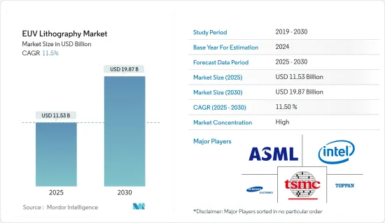
預計 2025 年 EUV微影術市場規模為 115.3 億美元,到 2030 年將達到 198.7 億美元,預測期內(2025-2030 年)的複合年成長率為 11.5%。
EUV微影術使用的光波長僅 13.5nm。這比先進晶片製造中的另一種微影術技術——使用 193nm 光的深紫外光微影術的波長短近 14 倍。該技術能夠更精確、更有效率地生產節點尺寸為 7nm 的半導體,甚至小至 5nm 的電晶體規模。
主要亮點
- 隨著半導體尺寸不斷縮小,採用 EUV微影術技術變得越來越重要。 EUV微影術技術能夠實現晶圓上複雜圖案的微型化,為5G、AI、汽車等次世代應用程式提供最佳且高效的選擇。借助 EUV 技術,EUV 光的短波長使得列印與先進技術相關的設計的奈米級特徵成為可能,使晶片製造商能夠繼續推動晶片小型化。
- 台積電的極紫外線 (EUV) 工具預計將達到生產成熟度,工具運轉率已達到量產目標,並在常規運行中提供超過 250 瓦的功率輸出。晶片製造商正在尋求利用 EUV 來實現 7nm、5nm 及更先進的邏輯,目前沒有其他選擇。下一代微影術技術尚未準備好,無法應用於7nm和5nm規模。對於 3nm 及以上,晶片製造商希望使用高 NA EUV,但開發這項技術仍面臨一些挑戰。
- 台積電也計劃在 2022 年開始量產 3nm 產品。另一家主要企業三星電子則計劃在 2030 年之前在極紫外線 (EUV)微影術技術方面超越台積電。台積電先前在 2019 年 12 月宣布,將於 2020 年上半年開始供應 5nm 製程晶片,並於 2022 年開始量產 3nm 製程晶片。該公司還預計在 2024 年開始生產 2nm 製程產品。
- 受新冠疫情影響,ASML 的設備出口出現困難,對三星電子、台積電等全球主要半導體製造商產生了不利影響。該公司的設備交付延遲迫使兩家公司改變其策略發展和生產藍圖。公司設備交付的延遲迫使兩家公司改變其策略發展和生產計畫。台積電延後了3奈米半導體的試產。同時,三星電子原計劃於 2020 年開始商業化生產 5nm 半導體,但直到 2021 年底才得以實現。
EUV微影術市場趨勢
鑄件製造商預計將佔據較大佔有率
- 台積電計畫於2022年開始量產3nm產品,因而稱霸全球晶圓代工廠市場。市場落後的三星電子則計劃在2030年極紫外線(EUV)微影術技術方面超越台積電。 2019年12月,台積電宣布將於2020年上半年開始供應5nm製程晶片,並於2022年開始量產3nm製程晶片。同時,台積電也預計2024年開始生產2nm製程產品。
- 三星在市場上面臨一系列挑戰。例如,用於 EUV微影術的光阻劑供應可能受到日本出口管制。此外,還有相當多的公司正在試圖與三星電子競爭。中國大陸和台灣的半導體公司合作日益密切。三星電子不斷推出新的微製造技術,如 FinFET、環柵和多橋通道 FET,以與越來越多的競爭對手競爭。
- 2021 年 2 月,三星代工向亞利桑那州、紐約州和德克薩斯州的當局提交了文件,尋求在美國建立一座尖端半導體製造工廠。該工廠將建在德克薩斯州奧斯汀附近,預計耗資超過 170 億美元,並創造 1,800 個就業機會。如果一切按計劃進行,該代工廠預計將於 2023 年第四季運作。該公司並未透露將針對哪種製程節點進行設計,但這家新晶圓廠很引人注目。
- 台灣半導體製造公司(TSMC)和聯華電子公司(UMC)等供應商已宣布,他們正專注於轉移生產,以滿足大眾和豐田等汽車製造商的需求。此外,高通和蘋果等公司的需求導致半導體供應延遲。 《汽車新聞》的一項新調查(2021 年 4 月)顯示,53% 的受訪者在美國境外採購晶片,55% 的製造商正在尋找海外替代晶片採購。
- 這些因素導致新公司進入研究市場。例如,英特爾最近宣布推出一項新業務——英特爾代工服務,以滿足汽車製造商的需求。同樣,2021年3月,World Castings表示將投資14億美元在全球擴大產能,以協助福特、福斯和通用汽車等汽車製造商削減產量。
預計亞太地區將佔很大佔有率
- 亞太地區持續佔據全球極紫外線(EUV)微影術市場的最大收入佔有率。預計台灣將在預測期內佔據該地區的主導地位。台積電在台灣的業務擴張以及加大對EUV微影術技術的投資是支撐台灣極紫外光微影術市場成長的最重要因素之一。台灣佔據了亞太地區EUV微影術市場的大部分收益佔有率。除台灣以外,日本、中國和韓國的極紫外光微影術市場預計將在未來幾年為相關人員提供重大機會。
- 隨著美國貿易摩擦加劇,中國半導體廠商也利用二手晶片製造設備加速生產自家產品,推高了日本二手市場的設備價格。日本二手設備經銷商表示,價格比去年上漲了 20%。老一輩的機器不受美國美國制裁的限制,所以中國玩家可以自由使用。
- 由於冠狀病毒大流行而傾向於待在室內也是一個因素。隨著全球對晶片的需求不斷成長,即使是不太先進的設備也賣得非常火爆。因此,汽車用半導體的供不應求有可能將長期持續。
- ASML 的新訓練設施可能對兩家公司都有好處。該公司是歐洲最大的半導體機械品牌,但台灣製造商是其最大客戶。根據《亞洲日經評論》報道,ASML今年計畫出貨的35台EUV系統當中,有20台是為台積電提供的。荷蘭公司 ASML 正在為晶片製造商的員工提供更多工具熟悉度,為未來的銷售做準備。 ASML 還計劃在台灣開設一個新的研發機構,到 2023 年將本地員工人數增加到 500 多人。
EUV微影術產業概況
EUV微影術市場高度整合,因為 ASML 是唯一一家使用極紫外光的微影術設備製造商。該公司為世界各地的半導體製造商生產和銷售設備,其中包括英特爾、三星和台灣半導體製造股份有限公司 (TSMC)。該公司近25%的企業收益來自EUV光刻工具的銷售,反映了該公司在EUV光刻工具製造和商業化方面的主導地位。
- 2021年12月歐洲新星ASML正在研發新版極紫外光微影術設備。該設備用於將圖案切割成矽塊,以製造世界上最複雜的處理器。三星、台積電和英特爾正在使用該公司目前的 EUV 設備為下一代電腦和智慧型手機製造晶片。
- 2021年3月三星將增加EUV掃描器的產量,以與全球最大的代工廠台積電競爭。與傳統設備不同,EUV 掃描器有可能透過減少生產更小電路所需的微影術步驟來簡化晶片製造流程,從而引發主要晶片製造商對該技術的競相爭奪。
其他福利:
- Excel 格式的市場預測 (ME) 表
- 3個月的分析師支持
目錄
第1章 引言
- 研究假設和市場定義
- 研究範圍
第2章調查方法
第3章執行摘要
第4章 市場洞察
- 市場概覽
- 產業價值鏈分析
- 產業吸引力-波特五力分析
- 供應商的議價能力
- 買家的議價能力
- 新進入者的威脅
- 替代品的威脅
- 競爭對手之間的競爭強度
- COVID-19 產業影響評估
第5章市場動態
- 市場促進因素
- 與其他技術相比,該技術可以更快地生產微晶片
- 晶片製造商減少製造步驟以提高效率
- 市場限制
- 使用 EUV 雷射器替換現有深紫外線雷射的高成本
- 市場壟斷
- 技術簡介
第6章市場區隔
- 產品類型
- 光源
- 鏡子
- 面具
- 類型
- 鑄件
- 整合設備製造商 (IDM)
- 地區
- 韓國
- 台灣
- 其他
第7章競爭格局
- 公司簡介
- ASML Holding NV
- NTT Advanced Technology Corporation
- Canon Inc.
- Nikon Corporation
- Intel Corporation
- Taiwan Semiconductor Manufacturing Company Limited
- Samsung Electronics Co. Ltd
- Toppan Photomasks Inc.
- Ushio, Inc.
第8章投資分析
第9章:市場的未來
The EUV Lithography Market size is estimated at USD 11.53 billion in 2025, and is expected to reach USD 19.87 billion by 2030, at a CAGR of 11.5% during the forecast period (2025-2030).
EUV lithography makes the usage of light with a wavelength of just 13.5 nm, which is a reduction of almost 14 times the wavelength of the other lithography techniques in advanced chipmaking, Deep Ultraviolet lithography, which uses 193 nm light. ASML, which is the dominant player in the market, has been exploring ways to reduce transistor sizes and has made considerable strides in the field of EUV lithography, which enables more precise and efficient production of semiconductors at small transistor scales around 7nm node size or even 5nm.
Key Highlights
- As semiconductor geometries tend to grow smaller and smaller, the adoption of EUV lithography technology has become extremely important, as it enables scaling down of intricate patterns on wafers by providing an optimal and efficient choice for next-generation applications, including 5G, AI, and Automotive. EUV technology allows the chip makers to keep driving chip scaling as the shorter wavelength of EUV light is capable of printing the nanometer-scale features of the designs related to the advanced techniques.
- TSMC's Extreme Ultraviolet (EUV) tools are expected to reach production maturity, with tool availability already reaching target goals for high-volume production and output power of greater than 250 watts for daily operations. Chipmakers are banking on EUV at 7nm, 5nm, and beyond for leading-edge logic, and today there are no other options available. The next-generation lithography technologies are not ready and can not be applied at 7nm and 5nm scales. At 3nm and beyond, chipmakers hope to use high-NA EUV, but several challenges have yet to be overcome in developing this technology.
- TSMC has also been planning to start the volume production of the 3-nm products by 2022. Samsung Electronics Co. Ltd, another major player in the market, aims to overtake TSMC by 2030 with its extreme ultraviolet (EUV) lithography technology. TSMC, previously in Dec 2019, announced that the company would be starting to supply 5 Nm process-based chips in the first half of 2020 and will be starting mass production of 3-nm process chips in 2022. The company also anticipates producing 2-nm process products by 2024.
- ASML faced difficulty exporting its equipment due to COVID-19, negatively affecting major global semiconductor producers, including Samsung Electronics and TSMC. A delay in the company's equipment delivery is forcing the two companies to change their strategic development and production roadmaps. Due to a delay in the delivery of the company's equipment, the two companies have to alter their strategic development and production plans. TSMC has postponed the test production of 3-nm semiconductors. Samsung Electronics, meantime, had hoped to commence commercial production of 5-nm semiconductors in 2020 but was unable to do so until late 2021.
EUV Lithography Market Trends
Foundry is Expected to Hold Major Share
- TSMC is planning to dominate the global foundry market by starting the volume production of 3-nm products in 2022. Samsung Electronics Co, Ltd, the runner-up in the market, is aiming to overtake TSMC in 2030 with its extreme ultraviolet (EUV) lithography technology. TSMC announced in December 2019 that the company would start to supply 5-nm process-based chips in the first half of 2020 and start the mass production of 3-nm process chips in 2022. The company also expects o produce 2-nm process products in 2024.
- Samsung is facing a series of challenges in the market. For instance, the supply of photoresists for EUV lithography purposes can be subject to Japan's export restrictions. Besides, a significant number of companies are trying to compete with Samsung Electronics. Chinese and Taiwanese semiconductor companies are increasingly collaborating. Samsung Electronics has unveiled a series of new microfabrication techniques such as FinFET, gate-all-around, and multi-bridge-channel FET to compete with the increasing competitors.
- In February 2021, Samsung Foundry filed documents with authorities in Arizona, New York, and Texas seeking to build a leading-edge semiconductor manufacturing facility in the United States. The potential fab near Austin, Texas, is expected to cost over USD 17 billion and create 1,800 jobs. If everything goes as planned, the foundry will go online by the fourth quarter of 2023. There is an intrigue about the new fab, though the company did not state which process node it will be designed for.
- Vendors, such as Taiwan Semiconductor Manufacturing Co. (TSMC) and United Microelectronics Corp. (UMC), announced that they have been focusing on relocating their production to meet the demand from automakers, such as Volkswagen and Toyota, among others. In addition, the demand coming from companies, such as Qualcomm and Apple, has been creating delays in the supply of semiconductors. According to a new survey by Automotive News (April 2021), 53% of the respondents suggested that they source their chips from outside the United States, and 55% of the manufacturers have been looking for alternative chip sources outside the country.
- Such factors have been leading to the entry of new companies into the market studied. For instance, recently, Intel announced the launch of a new business Intel Foundry Services, to meet the demand for automotive manufacturers. Similarly, in March 2021, Global Foundries announced that it has been planning to invest USD 1.4 billion for capacity expansion in different parts of the world to support automakers cutting output, such as Ford, Volkswagen, and General Motors.
Asia Pacific is Expected to Hold Major Share
- The Asia Pacific continues to hold the largest revenue share in the global market for Extreme Ultraviolet (EUV) lithography. Taiwan is expected to have an edge in the region over the forecast period. TSMC's expansion in Taiwan and its increasing investments in the EUV lithography technology is among the most critical factors instrumental in the growth of the Extreme Ultraviolet lithography market in Taiwan. The country accounts for the majority revenue share of the market for EUV lithography in the Asia Pacific region. Apart from Taiwan, the Extreme Ultraviolet lithography markets in Japan, China, and South Korea are expected to create significant opportunities for stakeholders in the coming years.
- Chinese semiconductor makers are also utilizing used chipmaking machines as they rush to produce homegrown products amid US-Sino trade tensions, driving up equipment prices in Japan's secondary market. Japanese used equipment dealers say prices are up by 20% from last year. Older-generation machines are not restricted by the United States sanctions on China, giving Chinese players unfettered access.
- The stay-at-home trend spurred by the coronavirus pandemic is also a factor. As chip demand rises worldwide, even equipment that is not the most up-to-date is selling at a brisk pace. This, in turn, could prolong the shortage of semiconductors used in automobiles.
- ASML's new training complex will likely be beneficial to both companies. While the firm is Europe's largest semiconductor machinery brand, the Taiwanese manufacturer is its biggest customer. Asian Nikkei Review states that 20 of the 35 EUV systems ASML intends to ship this year are going to TSMC. The Dutch concern is setting up future sales by familiarizing more of the chipmaker's staff with its tools. ASML also plans on opening a new research and development facility in Taiwan, which will bring its local headcount over 500 by 2023.
EUV Lithography Industry Overview
The Extreme Ultraviolet Lithography Market is highly consolidated as ASML is the only manufacturer of lithography machines that use extreme ultraviolet light. The company manufactures and sells its tools to some global semiconductor fabricators, including Intel, Samsung, and Taiwan Semiconductor Manufacturing Company (TSMC). Almost 25% of the company's revenues are generated by sales of EUV lithography systems, which reflects the company's monopoly in the manufacturing and commercialization of EUV lithography systems.
- December 2021: ASML, a hot stock in Europe, is working on a new version of their extreme ultraviolet lithography equipment, which is used to carve patterns into chunks of silicon that produce the world's most sophisticated processors. Samsung, TSMC, and Intel use the company's current EUV equipment to create chips for the next generation of computers and smartphones.
- March 2021: Samsung is increasing its EUV scanner production to compete with TSMC, the world's largest foundry. EUV scanners, unlike traditional machines, may streamline the chip fabrication process by lowering the number of photolithography procedures necessary to generate finer circuits, causing major chipmakers to compete for the technology.
Additional Benefits:
- The market estimate (ME) sheet in Excel format
- 3 months of analyst support
TABLE OF CONTENTS
1 INTRODUCTION
- 1.1 Study Assumptions and Market Definition
- 1.2 Scope of the Study
2 RESEARCH METHODOLOGY
3 EXECUTIVE SUMMARY
4 MARKET INSIGHTS
- 4.1 Market Overview
- 4.2 Industry Value Chain Analysis
- 4.3 Industry Attractiveness - Porter's Five Forces Analysis
- 4.3.1 Bargaining Power of Suppliers
- 4.3.2 Bargaining Power of Buyers
- 4.3.3 Threat of New Entrants
- 4.3.4 Threat of Substitute Products
- 4.3.5 Intensity of Competitive Rivalry
- 4.4 Assessment of COVID-19 Impact on the Industry
5 MARKET DYNAMICS
- 5.1 Market Drivers
- 5.1.1 The technology resulting in a faster output of microchips compared to others
- 5.1.2 Chip makers reducing the manufacturing process for better efficiency
- 5.2 Market Restraints
- 5.2.1 High cost involved in replacing the existing Deep UV with EUV lasers
- 5.2.2 Monopoly existing within the market
- 5.3 Technology Snapshot
6 MARKET SEGMENTATION
- 6.1 Product Type
- 6.1.1 Light Sources
- 6.1.2 Mirrors
- 6.1.3 Masks
- 6.2 Type
- 6.2.1 Foundry
- 6.2.2 Integrated Device Manufacturers (IDMs)
- 6.3 Geography
- 6.3.1 South Korea
- 6.3.2 Taiwan
- 6.3.3 Others
7 COMPETITIVE LANDSCAPE
- 7.1 Company Profiles
- 7.1.1 ASML Holding NV
- 7.1.2 NTT Advanced Technology Corporation
- 7.1.3 Canon Inc.
- 7.1.4 Nikon Corporation
- 7.1.5 Intel Corporation
- 7.1.6 Taiwan Semiconductor Manufacturing Company Limited
- 7.1.7 Samsung Electronics Co. Ltd
- 7.1.8 Toppan Photomasks Inc.
- 7.1.9 Ushio, Inc.
8 INVESTMENT ANALYSIS
9 FUTURE OF THE MARKET
 雷射氣體光刻市場分析及預測(至2035年):依類型、產品類型、服務、技術、組件、應用、材料類型、製程、最終用戶及設備分類
 極紫外線 (EUV) 微影市場:依設備(曝光系統、光源、光學元件和反射鏡、掩模相關系統)、技術(標準 EUV/NXE、高數值孔徑 EUV/EXE)和應用(代工廠、記憶體、整合裝置製造商)劃分 - 全球預測至 2036 年
 全球極紫外光刻市場規模、佔有率、趨勢和成長分析報告(2026-2034年)
 極紫外線(EUV)微影術市場:按組件、系統類型、最終用戶、應用和地區分類的全球市場-預測至2032年
 全球極微影術元件市場:預測(至2034年)-按裝置類型、材料類型、技術、應用、最終使用者和地區分類的分析
 2026年全球極紫外光微影市場報告
 半色調掩模市場按掩模類型、最終用途行業和分銷管道分類 - 全球預測 2026-2032極紫外平面鏡市場:依基板、鍍膜材料、應用及通路分類,全球預測(2026-2032年)極紫外光刻 (EUV) 市場規模、佔有率、成長及全球產業分析:按類型、應用和地區劃分的洞察與預測 (2026-2034)
 極紫外光刻市場-全球產業規模、佔有率、趨勢、機會及預測(依技術節點、組件類型、終端用戶產業、區域及競爭格局分類,2021-2031年預測)