

 |
市場調查報告書
商品編碼
1740912
雷射光刻系統市場機會、成長動力、產業趨勢分析及 2025 - 2034 年預測Laser Lithography Systems Market Opportunity, Growth Drivers, Industry Trend Analysis, and Forecast 2025 - 2034 |
||||||
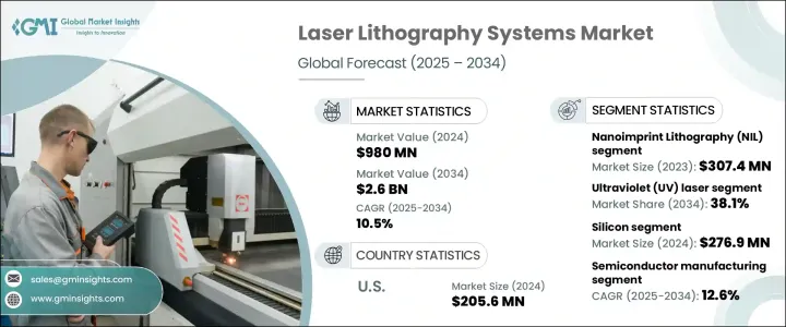
2024 年,全球雷射光刻系統市場規模達 9.8 億美元,預計到 2034 年將以 10.5% 的複合年成長率成長,達到 26 億美元,這主要得益於市場對更強大、更緊湊、更節能的半導體裝置日益成長的需求。隨著半導體技術的進步不斷突破微型化和性能的界限,該市場正獲得顯著發展動能。隨著晶片製造商積極追求更小的節點,雷射光刻系統(尤其是深紫外線 (DUV) 和極紫外線 (EUV) 系統)對於提供下一代生產所需的精度和可擴展性至關重要。人工智慧、電信和高效能消費性電子產品領域正在向 10 奈米以下技術轉變,凸顯了對超高精度圖案化解決方案的需求。
隨著莫耳定律持續推動製造商創新,雷射光刻技術為大規模生產複雜、高密度元件提供了技術支撐。研發投入、5G基礎設施的普及、物聯網的擴展以及光子學日益融入主流應用,進一步增強了市場前景。晶片製造領域對永續性和能源效率的日益重視,也有利於先進的光刻解決方案,推動了從傳統方法向基於雷射的系統顯著轉變,該系統可提供更高的吞吐量、更低的缺陷率和更好的材料利用率。
| 市場範圍 | |
|---|---|
| 起始年份 | 2024 |
| 預測年份 | 2025-2034 |
| 起始值 | 9.8億美元 |
| 預測值 | 26億美元 |
| 複合年成長率 | 10.5% |
隨著 10 奈米以下節點技術在人工智慧、電信和高性能消費性電子產品中的應用日益廣泛,雷射光刻——深紫外線 (DUV) 和極紫外線 (EUV) 系統——已成為實現晶片精密圖案化的關鍵。隨著半導體製造商不斷縮小電晶體尺寸以遵循莫耳定律,下一代光刻解決方案需要提供維持生產效率和滿足市場需求所需的精度和解析度。
系統單晶片 (SoC) 和光子積體電路 (PIC) 等整合系統的興起帶來了新的設計挑戰,只有採用高度先進的雷射光刻技術才能應對。這些電路需要卓越的圖案化精度,尤其是在醫療診斷、電信和汽車安全系統等應用領域。光波導、微光學元件和感測器等光子和光電子裝置依賴超精密的製造製程。雷射光刻技術的創新使得建構用於快速資料通訊、雷射雷達 (LiDAR) 技術和高解析度醫學成像的奈米結構成為可能。
2024年,雷射光刻系統市場中矽晶片的部分規模達到2.769億美元。由於矽晶圓與CMOS製程的出色相容性、成本效益以及優異的電氣特性,它仍然是整個半導體產業的首選基板。隨著先進電子產品規模的不斷擴大,矽晶圓在邏輯電路、微控制器和儲存晶片中的廣泛應用確保了其穩定的需求。隨著人工智慧運算、資料中心和下一代行動裝置等領域對精度的要求日益提高,矽晶圓的多功能性使其能夠支援高密度、高速的元件。
預計半導體製造領域將迎來強勁發展勢頭,2025 年至 2034 年期間的複合年成長率將達到 12.6%。這一成長與高效能運算、人工智慧晶片以及需要奈米級超精細圖案化的下一代記憶體解決方案日益成長的需求密切相關。雷射光刻技術,尤其是使用 EUV(極紫外線)和 DUV(深紫外線)技術的雷射光刻技術,是這些技術進步的核心。這些系統可實現 5 奈米以下節點的生產,這是突破莫耳定律極限的關鍵基準。
在政府大力推動半導體生產回流政策的推動下,美國雷射光刻系統市場規模在2024年達到2.056億美元。聯邦政府的資金投入和跨部門合作正在加速奈米製造技術的突破,使美國成為技術進步的關鍵樞紐。
Raith GmbH、海德堡儀器和 KLA Corporation 等領先企業的關鍵策略包括增強研發能力、與研究機構合作以及擴大生產能力。這些公司正在投資超解析度雷射系統,並針對 10 奈米以下製造、PIC 生產和混合封裝等高成長領域最佳化其產品。此外,與半導體代工廠的合作也有助於這些公司在高度動態的市場中保持敏捷。
目錄
第1章:方法論與範圍
第2章:執行摘要
第3章:行業洞察
- 產業生態系統分析
- 影響價值鏈的因素
- 利潤率分析
- 中斷
- 未來展望
- 製造商
- 經銷商
- 川普政府關稅對飛機零件的影響分析
- 對貿易的影響
- 貿易量中斷
- 報復措施
- 對產業的影響
- 供給側影響
- 價格波動
- 供應鏈重組
- 生產成本影響
- 需求面影響
- 價格傳導至終端市場
- 消費者反應模式
- 供給側影響
- 受影響的主要公司
- 策略產業回應
- 供應鏈重組
- 定價和產品策略
- 政策參與
- 展望與未來考慮
- 對貿易的影響
- 供應商格局
- 利潤率分析
- 重要新聞和舉措
- 監管格局
- 衝擊力
- 成長動力
- 半導體小型化需求不斷成長
- 極紫外線 (EUV) 微影技術的進步
- 光子學和光電子學領域的應用日益廣泛
- 先進封裝技術的擴展
- 政府對半導體製造的支持
- 產業陷阱與挑戰
- 資本和營運成本高
- 技術複雜性和工藝限制
- 成長動力
- 成長潛力分析
- 波特的分析
- PESTEL分析
第4章:競爭格局
- 介紹
- 公司市佔率分析
- 競爭定位矩陣
- 戰略展望矩陣
第5章:市場估計與預測:依技術類型,2021-2034
- 主要趨勢
- 直接雷射寫入(DLW)
- 干涉光刻
- 奈米壓印微影術(NIL)
- 雙光子聚合(2PP)
第6章:市場估計與預測:按雷射光源,2021-2034 年
- 主要趨勢
- 準分子雷射
- 二極體雷射
- 飛秒雷射
- 紫外線(UV)雷射
第7章:市場估計與預測:依基材類型,2021-2034
- 主要趨勢
- 矽
- 玻璃
- 聚合物
- 金屬
第 8 章:市場估計與預測:按應用,2021 年至 2034 年
- 主要趨勢
- 半導體製造
- 微電子
- 光子裝置
- 微流體
- 顯示器技術(OLED、MicroLED、LCD 等)
- 奈米科技研究
- 生物技術和醫療器械
第9章:市場估計與預測:依最終用途產業,2021-2034 年
- 主要趨勢
- 電子和半導體
- 醫療保健和生物醫學
- 航太與國防
- 汽車
- 電信
- 其他
第10章:市場估計與預測:按地區,2021-2034
- 主要趨勢
- 北美洲
- 美國
- 加拿大
- 歐洲
- 英國
- 德國
- 法國
- 義大利
- 西班牙
- 俄羅斯
- 亞太地區
- 中國
- 印度
- 日本
- 韓國
- 澳洲
- 拉丁美洲
- 巴西
- 墨西哥
- MEA
- 南非
- 沙烏地阿拉伯
- 阿拉伯聯合大公國
第 11 章:公司簡介
- ADVANTEST CORPORATION
- AGC Inc.
- ASML Holding NV
- Carl Zeiss AG
- Edmund Optics Inc.
- Energetiq Technology, Inc.
- Finisar
- Heidelberg Instruments
- HOYA Corporation
- INTEGRATED DYNAMICS ENGINEERING GmbH
- KLA Corporation
- Lasertec Corporation
- NTT Advanced Technology Corporation
- NuFlare Technology Inc.
- Onto Innovation Inc.
- Photronics, Inc.
- Raith GmbH
- Rigaku Holdings Corporation
- Sono-Tek Corporation
- SUSS MicroTec SE
- TOPPAN Inc.
- TRUMPF
- TSI
- Ushio Inc.
- Veeco Instruments, Inc.
The Global Laser Lithography Systems Market was valued at USD 980 million in 2024 and is estimated to grow at a CAGR of 10.5% to reach USD 2.6 billion by 2034, driven by the rising demand for more powerful, compact, and energy-efficient semiconductor devices. The market is gaining significant momentum as advancements in semiconductor technology push the boundaries of miniaturization and performance. With chipmakers aggressively pursuing smaller nodes, the role of laser lithography systems-especially deep ultraviolet (DUV) and extreme ultraviolet (EUV) systems-has become critical for delivering the precision and scalability needed for next-generation production. The ongoing shift toward sub-10nm technologies across artificial intelligence, telecommunications, and high-performance consumer electronics underscores the need for ultra-accurate patterning solutions.
As Moore's Law continues to pressure manufacturers to innovate, laser lithography provides the technological backbone for producing complex, high-density devices at scale. Investments in R&D, rising adoption of 5G infrastructure, IoT expansion, and the increasing integration of photonics into mainstream applications further strengthen the market outlook. The growing emphasis on sustainability and energy efficiency in chip manufacturing also favors advanced lithography solutions, driving a notable shift from traditional methods to laser-based systems that offer higher throughput, lower defect rates, and better material utilization.
| Market Scope | |
|---|---|
| Start Year | 2024 |
| Forecast Year | 2025-2034 |
| Start Value | $980 Million |
| Forecast Value | $2.6 Billion |
| CAGR | 10.5% |
With the increasing adoption of sub-10nm node technology in artificial intelligence, telecommunications, and high-performance consumer electronics, laser lithography-deep ultraviolet (DUV) and extreme ultraviolet (EUV) systems-has become vital for precision chip patterning. As semiconductor manufacturers continue shrinking transistor dimensions to adhere to Moore's Law, next-generation lithography solutions offer the accuracy and resolution needed to sustain production efficiency and meet market demand.
The rise of integrated systems such as system-on-chip (SoC) and photonic integrated circuits (PICs) presents new design challenges that can only be addressed with highly advanced laser-based lithography techniques. These circuits demand exceptional patterning accuracy, especially as they are used in applications ranging from healthcare diagnostics to telecommunications and automotive safety systems. Photonic and optoelectronic devices, such as optical waveguides, micro-optics, and sensors, rely on ultra-precise fabrication processes. Innovations in laser lithography enable the construction of nanostructures used in fast data communication, LiDAR technologies, and high-resolution medical imaging.
The silicon segment in the laser lithography systems market reached USD 276.9 million in 2024. Silicon remains the preferred substrate across the semiconductor industry due to its excellent compatibility with CMOS processes, cost-effectiveness, and superior electrical characteristics. Its widespread use in logic circuits, microcontrollers, and memory chips ensures a steady demand as advanced electronics continue to scale. As precision requirements intensify in fields like AI computing, data centers, and next-generation mobile devices, silicon's versatility enables it to support high-density, high-speed components.
The semiconductor manufacturing segment is expected to experience strong momentum, with a projected CAGR of 12.6% between 2025 and 2034. This growth is closely linked to the rising demand for high-performance computing, AI chips, and next-gen memory solutions that require ultra-fine patterning at the nanoscale. Laser lithography, especially using EUV (extreme ultraviolet) and DUV (deep ultraviolet) technologies, is at the core of these advancements. These systems allow for sub-5nm node production, a critical benchmark in pushing the limits of Moore's Law.
United States Laser Lithography Systems Market reached USD 205.6 million in 2024, supported by robust government policies focused on reshoring semiconductor production. Federal funding and cross-sector partnerships are accelerating breakthroughs in nanofabrication, making the country a critical hub for technological advancement.
Key strategies among leading players-Raith GmbH, Heidelberg Instruments, KLA Corporation-include expanding R&D capabilities, collaborating with research institutes, and scaling manufacturing capacity. Companies are investing in ultra-resolution laser systems and optimizing their offerings for high-growth areas like sub-10nm fabrication, PIC production, and hybrid packaging. Additionally, partnerships with semiconductor foundries are helping these firms remain agile in a highly dynamic market.
Table of Contents
Chapter 1 Methodology & Scope
- 1.1 Market scope & definitions
- 1.2 Base estimates & calculations
- 1.3 Forecast calculations
- 1.4 Data sources
- 1.4.1 Primary
- 1.4.2 Secondary
- 1.4.2.1 Paid sources
- 1.4.2.2 Public sources
Chapter 2 Executive Summary
- 2.1 Industry synopsis, 2021-2034
Chapter 3 Industry Insights
- 3.1 Industry ecosystem analysis
- 3.1.1 Factor affecting the value chain
- 3.1.2 Profit margin analysis
- 3.1.3 Disruptions
- 3.1.4 Future outlook
- 3.1.5 Manufacturers
- 3.1.6 Distributors
- 3.2 Trump Administration Tariffs Impact Analysis on Aircraft Components
- 3.2.1 Impact on Trade
- 3.2.1.1 Trade Volume Disruptions
- 3.2.1.2 Retaliatory Measures
- 3.2.1.3 Impact on the Industry
- 3.2.1.3.1 Supply-Side Impact
- 3.2.1.3.1.1 Price Volatility
- 3.2.1.3.1.2 Supply Chain Restructuring
- 3.2.1.3.1.3 Production Cost Implications
- 3.2.1.3.2 Demand-Side Impact
- 3.2.1.3.2.1 Price Transmission to End Markets
- 3.2.1.3.2.2 Consumer Response Patterns
- 3.2.1.3.1 Supply-Side Impact
- 3.2.1.4 Key Companies Impacted
- 3.2.1.5 Strategic Industry Responses
- 3.2.1.5.1 Supply chain reconfiguration
- 3.2.1.5.2 Pricing and product strategies
- 3.2.1.5.3 Policy engagement
- 3.2.1.6 Outlook and future considerations
- 3.2.1 Impact on Trade
- 3.3 Supplier landscape
- 3.4 Profit margin analysis
- 3.5 Key news & initiatives
- 3.6 Regulatory landscape
- 3.7 Impact forces
- 3.7.1 Growth drivers
- 3.7.1.1 Rising demand for semiconductor miniaturization
- 3.7.1.2 Advancements in Extreme Ultraviolet (EUV) lithography
- 3.7.1.3 Growing adoption in photonics and optoelectronics
- 3.7.1.4 Expansion of advanced packaging technologies
- 3.7.1.5 Government support for semiconductor manufacturing
- 3.7.2 Industry pitfalls & challenges
- 3.7.2.1 High capital and operational costs
- 3.7.2.2 Technical complexity and process limitations
- 3.7.1 Growth drivers
- 3.8 Growth potential analysis
- 3.9 Porter's analysis
- 3.10 PESTEL analysis
Chapter 4 Competitive Landscape, 2024
- 4.1 Introduction
- 4.2 Company market share analysis
- 4.3 Competitive positioning matrix
- 4.4 Strategic outlook matrix
Chapter 5 Market Estimates & Forecast, By Technology Type, 2021-2034 (USD Million)
- 5.1 Key trends
- 5.2 Direct Laser Writing (DLW)
- 5.3 Interference lithography
- 5.4 Nanoimprint Lithography (NIL)
- 5.5 Two-Photon Polymerization (2PP)
Chapter 6 Market Estimates & Forecast, By Laser Source, 2021-2034 (USD Million)
- 6.1 Key trends
- 6.2 Excimer laser
- 6.3 Diode laser
- 6.4 Femtosecond laser
- 6.5 Ultraviolet (UV) laser
Chapter 7 Market Estimates & Forecast, By Substrate Type, 2021-2034 (USD Million)
- 7.1 Key trends
- 7.2 Silicon
- 7.3 Glass
- 7.4 Polymers
- 7.5 Metal
Chapter 8 Market Estimates & Forecast, By Application, 2021-2034 (USD Million)
- 8.1 Key trends
- 8.2 Semiconductor manufacturing
- 8.3 Microelectronics
- 8.4 Photonic Devices
- 8.5 Microfluidics
- 8.6 Display Technology (OLED, MicroLEDs, LCDs, etc.)
- 8.7 Nanotechnology research
- 8.8 Biotechnology & medical devices
Chapter 9 Market Estimates & Forecast, By End Use Industry, 2021-2034 (USD Million)
- 9.1 Key trends
- 9.2 Electronics & semiconductor
- 9.3 Healthcare & biomedical
- 9.4 Aerospace & defense
- 9.5 Automotive
- 9.6 Telecommunications
- 9.7 Others
Chapter 10 Market Estimates & Forecast, By Region, 2021-2034 (USD Million)
- 10.1 Key trends
- 10.2 North America
- 10.2.1 U.S.
- 10.2.2 Canada
- 10.3 Europe
- 10.3.1 UK
- 10.3.2 Germany
- 10.3.3 France
- 10.3.4 Italy
- 10.3.5 Spain
- 10.3.6 Russia
- 10.4 Asia Pacific
- 10.4.1 China
- 10.4.2 India
- 10.4.3 Japan
- 10.4.4 South Korea
- 10.4.5 Australia
- 10.5 Latin America
- 10.5.1 Brazil
- 10.5.2 Mexico
- 10.6 MEA
- 10.6.1 South Africa
- 10.6.2 Saudi Arabia
- 10.6.3 UAE
Chapter 11 Company Profiles
- 11.1 ADVANTEST CORPORATION
- 11.2 AGC Inc.
- 11.3 ASML Holding N.V.
- 11.4 Carl Zeiss AG
- 11.5 Edmund Optics Inc.
- 11.6 Energetiq Technology, Inc.
- 11.7 Finisar
- 11.8 Heidelberg Instruments
- 11.9 HOYA Corporation
- 11.10 INTEGRATED DYNAMICS ENGINEERING GmbH
- 11.11 KLA Corporation
- 11.12 Lasertec Corporation
- 11.13 NTT Advanced Technology Corporation
- 11.14 NuFlare Technology Inc.
- 11.15 Onto Innovation Inc.
- 11.16 Photronics, Inc.
- 11.17 Raith GmbH
- 11.18 Rigaku Holdings Corporation
- 11.19 Sono-Tek Corporation
- 11.20 SUSS MicroTec SE
- 11.21 TOPPAN Inc.
- 11.22 TRUMPF
- 11.23 TSI
- 11.24 Ushio Inc.
- 11.25 Veeco Instruments, Inc.
 極紫外光微影術市場:2026-2032年全球市場預測(依設備類型、應用、晶圓尺寸、最終用戶及抗蝕劑材料分類)
 雷射氣體光刻市場分析及預測(至2035年):依類型、產品類型、服務、技術、組件、應用、材料類型、製程、最終用戶及設備分類
 極紫外線 (EUV) 微影市場:依設備(曝光系統、光源、光學元件和反射鏡、掩模相關系統)、技術(標準 EUV/NXE、高數值孔徑 EUV/EXE)和應用(代工廠、記憶體、整合裝置製造商)劃分 - 全球預測至 2036 年
 全球極紫外光刻市場規模、佔有率、趨勢和成長分析報告(2026-2034年)
 極紫外線(EUV)微影術市場:按組件、系統類型、最終用戶、應用和地區分類的全球市場-預測至2032年
 全球極微影術元件市場:預測(至2034年)-按裝置類型、材料類型、技術、應用、最終使用者和地區分類的分析
 2026年全球極紫外光微影市場報告半色調掩模市場按掩模類型、最終用途行業和分銷管道分類 - 全球預測 2026-2032極紫外平面鏡市場:依基板、鍍膜材料、應用及通路分類,全球預測(2026-2032年)極紫外光刻 (EUV) 市場規模、佔有率、成長及全球產業分析:按類型、應用和地區劃分的洞察與預測 (2026-2034)