

 |
市場調查報告書
商品編碼
1766204
砷化鎵(GaAs)晶圓市場機會、成長動力、產業趨勢分析及2025-2034年預測Gallium Arsenide (GaAs) Wafer Market Opportunity, Growth Drivers, Industry Trend Analysis, and Forecast 2025 - 2034 |
||||||
2024年,全球砷化鎵晶圓市場規模達11.4億美元,預計2034年將以11.8%的複合年成長率成長,達到35.1億美元。這一成長主要歸功於5G技術的廣泛應用以及光子學和光電裝置的進步。砷化鎵憑藉其更高的電子遷移率和飽和速度,相較於矽等傳統材料更具優勢,適用於高頻和高速應用。隨著全球5G基礎設施的加速部署,對採用砷化鎵晶圓製造的射頻元件的需求急劇成長。
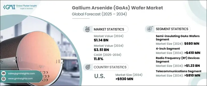
這些晶圓對於開發支援更快資料傳輸速率和更低延遲的新一代無線系統組件至關重要。除電信領域外,GaAs晶圓因其直接能隙特性,在光電應用中也被廣泛應用,從而支援高效的光發射和檢測。通訊網路的不斷發展,以及雷射技術和光電探測器應用的不斷拓展,顯著增強了主要經濟體GaAs晶圓市場的成長動能。對高性能電子產品和安全供應鏈的日益關注,也支持了這些晶圓在策略領域的應用。
| 市場範圍 | |
|---|---|
| 起始年份 | 2024 |
| 預測年份 | 2025-2034 |
| 起始值 | 11.4億美元 |
| 預測值 | 35.1億美元 |
| 複合年成長率 | 11.8% |
亞太地區正在成為砷化鎵晶圓的生產中心,多個國家正在大力投資下一代電信基礎設施,推動了對射頻元件的需求。受5G快速普及和對先進無線系統日益成長的需求的推動,北美也正經歷著強勁的發展勢頭。該地區日益依賴砷化鎵晶圓來增強高頻性能,凸顯了其在現代通訊中的戰略重要性。這種材料能夠有效地以最小的延遲處理大資料流,這使得它對下一代技術至關重要。同時,全球光電產業正利用砷化鎵優異的電子遷移率和能隙結構,繼續將其整合到LED、雷射發射器和光感測器等裝置中。
半絕緣GaAs晶圓(2024年價值6.8億美元)引領此細分市場,因為它們是建造射頻和微波元件的關鍵。其低載流子濃度和高電阻率使其成為製造射頻開關和放大器的理想選擇,這些裝置廣泛應用於各種高頻通訊平台。半絕緣GaAs晶圓能夠最大限度地降低訊號干擾,使其成為對精度和性能要求極高的環境中的首選。
預計到2034年,4吋GaAs晶圓市場規模將達到4.1億美元。這類晶圓仍是製造業的首選,這主要歸功於其與生產設備的良好相容性,以及在射頻和光電元件領域的高使用量。它們在市場上的長期存在確保了穩定的供應鏈,並易於整合到商業規模營運中,使其成為許多應用的標準。
受國防、航太和無線通訊領域日益成長的需求推動,美國砷化鎵 (GaAs) 晶圓市場規模預計在 2034 年達到 9.3 億美元。隨著美國優先考慮半導體的自主性和技術領先地位,公共和私人部門對增強 GaAs 基技術的投資正在加速。雷射雷達和衛星通訊等應用的日益普及,進一步推動了對 GaAs 晶圓的需求。扶持政策和專案研究正在推動創新,並提升該地區的國內生產能力。
積極影響砷化鎵 (GaAs) 晶圓市場的關鍵參與者包括 WIN Semiconductors Corp.、IQE plc、住友電工株式會社、VPEC Inc.(Visual Photonics Epitaxy Company)和東芝公司。 GaAs 晶圓市場的知名參與者正在部署各種策略方針,以保持競爭優勢並擴大其全球影響力。他們不斷投資研發,以提高晶圓品質、提高生產效率並增強設備性能。與終端使用產業的策略合作正在幫助公司更好地使其產品與不斷變化的應用需求保持一致。許多製造商也專注於擴大產能並建立區域製造中心,以滿足當地需求,同時最大限度地降低供應鏈風險。此外,各公司正在加強其智慧財產權組合併推進專有外延技術,以確保產品差異化。
目錄
第1章:方法論與範圍
第2章:執行摘要
第3章:行業洞察
- 產業生態系統分析
- 川普政府關稅
- 對貿易的影響
- 貿易量中斷
- 報復措施
- 對產業的影響
- 供給側影響(原料)
- 主要材料價格波動
- 供應鏈重組
- 生產成本影響
- 需求面影響(售價)
- 價格傳導至終端市場
- 市佔率動態
- 消費者反應模式
- 供給側影響(原料)
- 受影響的主要公司
- 策略產業反應
- 供應鏈重組
- 定價和產品策略
- 政策參與
- 展望與未來考慮
- 對貿易的影響
- 供應商矩陣
- 利潤率分析
- 技術與創新格局
- 專利分析
- 重要新聞和舉措
- 產業衝擊力
- 成長動力
- 高頻射頻設備需求不斷成長
- 光電子應用的擴展
- ADAS 和自動駕駛汽車的成長
- 太空和軍事通訊領域的應用
- 向更大晶圓尺寸(6吋)過渡
- 產業陷阱與挑戰
- 製造成本高且製造複雜
- 矽和 SiGe 技術進步
- 成長動力
- 成長潛力分析
- 監管格局
- 技術格局
- 未來市場趨勢
- 差距分析
- 波特的分析
- PESTEL分析
第4章:競爭格局
- 介紹
- 公司市佔率分析
- 主要市場參與者的競爭分析
- 競爭定位矩陣
- 策略儀表板
第5章:市場預估與預測:依晶圓類型,2021 - 2034
- 半絕緣GaAs晶片
- 半導體GaAs晶片
第6章:市場估計與預測:依晶圓尺寸,2021 - 2034
- 2英吋
- 4吋
- 6吋
- 8吋
第7章:市場估計與預測:按應用,2021 - 2034 年
- 射頻 (RF) 設備
- 光電裝置
- 光電設備
- 單晶片微波積體電路(MMIC)
第8章:市場估計與預測:依最終用途,2021 - 2034 年
- 電信
- 消費性電子產品
- 汽車
- 航太與國防
- 工業自動化
- 能源與電力
- 其他
第9章:市場估計與預測:按地區,2021 - 2034 年
- 主要趨勢
- 北美洲
- 美國
- 加拿大
- 歐洲
- 德國
- 英國
- 法國
- 西班牙
- 義大利
- 荷蘭
- 亞太地區
- 中國
- 印度
- 日本
- 澳洲
- 韓國
- 拉丁美洲
- 巴西
- 墨西哥
- 阿根廷
- 中東和非洲
- 沙烏地阿拉伯
- 南非
- 阿拉伯聯合大公國
第10章:公司簡介
- Analog Devices Inc.
- AWSC (Advanced Wireless Semiconductor Company)
- AXT Inc.
- Broadcom Inc.
- Coherent Corp.
- Cree (Wolfspeed)
- Freiberger Compound Materials GmbH
- Fujitsu Semiconductor Limited
- IntelliEPI Inc.
- IQE plc
- MACOM Technology Solutions
- Northrop Grumman Corporation
- Qorvo Inc.
- RFHIC Corporation
- Skyworks Solutions Inc.
- Sumitomo Electric Industries, Ltd.
- Toshiba Corporation
- VPEC Inc.
- WIN Semiconductors Corp.
The Global Gallium Arsenide Wafer Market was valued at USD 1.14 billion in 2024 and is estimated to grow at a CAGR of 11.8% to reach USD 3.51 billion by 2034. The growth is largely attributed to the widespread adoption of 5G technology and advancements in photonics and optoelectronic devices. Gallium arsenide offers advantages over traditional materials like silicon due to its higher electron mobility and saturation velocity, making it suitable for high-frequency and high-speed applications. As the rollout of 5G infrastructure accelerates globally, the demand for RF components built using GaAs wafers has risen sharply.
These wafers are essential for developing components that power next-gen wireless systems by supporting faster data transfer rates and lower latency. Apart from telecommunications, GaAs wafers are heavily utilized in optoelectronic applications due to their direct bandgap, which supports efficient light emission and detection. The ongoing development in communication networks, along with expanding uses in laser technologies and photodetectors, is significantly strengthening the growth trajectory of the GaAs wafer market across major economies. Increasing focus on high-performance electronics and secure supply chains is also supporting the adoption of these wafers in strategic sectors.
| Market Scope | |
|---|---|
| Start Year | 2024 |
| Forecast Year | 2025-2034 |
| Start Value | $1.14 Billion |
| Forecast Value | $3.51 Billion |
| CAGR | 11.8% |
The Asia-Pacific region is emerging as a hub for GaAs wafer production, with several countries investing heavily in next-generation telecom infrastructure, boosting demand for RF components. North America is also witnessing considerable momentum, driven by rapid 5G adoption and an increasing need for advanced wireless systems. The region's growing reliance on GaAs wafers to enhance high-frequency capabilities highlights their strategic importance in modern communications. The material's effectiveness in handling large data streams with minimal delay is making it increasingly essential to next-gen technologies. Meanwhile, the global optoelectronics sector continues to integrate gallium arsenide into devices like LEDs, laser emitters, and light sensors, leveraging its superior electron mobility and bandgap structure.
Semi-insulating GaAs wafers, valued at USD 680 million in 2024, lead the market segment because they are essential in building RF and microwave components. Their low carrier concentration and high resistivity make them perfect for fabricating RF switches and amplifiers, which are widely used across various high-frequency communication platforms. Their ability to minimize signal interference makes them a top choice in environments demanding precision and performance.
The 4-inch GaAs wafer segment is forecast to reach USD 410 million by 2034. These wafers remain the most preferred in manufacturing, largely because of their established compatibility with production equipment and high usage volumes in RF and optoelectronic components. Their longstanding presence in the market ensures a steady supply chain and ease of integration into commercial-scale operations, making them a standard for many applications.
United States Gallium Arsenide (GaAs) Wafer Market is poised to reach USD 930 million by 2034, fueled by growing demand from defense, aerospace, and wireless communication fields. Public and private investments in enhancing GaAs-based technologies are accelerating as the country prioritizes semiconductor independence and technological leadership. Increasing adoption in applications like LIDAR and satellite communication is further pushing the demand for GaAs wafers. Supportive policies and dedicated research are driving innovation and advancing domestic production capabilities in the region.
Key players actively shaping the Gallium Arsenide (GaAs) Wafer Market include WIN Semiconductors Corp., IQE plc, Sumitomo Electric Industries, Ltd., VPEC Inc. (Visual Photonics Epitaxy Company), and Toshiba Corporation. Prominent players in the GaAs wafer market are deploying a variety of strategic approaches to maintain a competitive edge and expand their global reach. They are consistently investing in R&D to improve wafer quality, increase production efficiency, and enhance device performance. Strategic collaborations with end-use industries are helping companies better align their offerings with evolving application needs. Many manufacturers are also focusing on capacity expansion and establishing regional manufacturing hubs to support local demand while minimizing supply chain risks. In addition, firms are strengthening their intellectual property portfolios and advancing proprietary epitaxy technologies to ensure product differentiation.
Table of Contents
Chapter 1 Methodology and Scope
- 1.1 Market scope and definitions
- 1.2 Research design
- 1.2.1 Research approach
- 1.2.2 Data collection methods
- 1.3 Base estimates and calculations
- 1.3.1 Base year calculation
- 1.3.2 Key trends for market estimation
- 1.4 Forecast model
- 1.5 Primary research and validation
- 1.5.1 Primary sources
- 1.5.2 Data mining sources
Chapter 2 Executive Summary
- 2.1 Industry 3600 synopsis
Chapter 3 Industry Insights
- 3.1 Industry ecosystem analysis
- 3.2 Trump administration tariffs
- 3.2.1 Impact on trade
- 3.2.1.1 Trade volume disruptions
- 3.2.1.2 Retaliatory measures
- 3.2.2 Impact on the industry
- 3.2.2.1 Supply-side impact (raw materials)
- 3.2.2.1.1 Price volatility in key materials
- 3.2.2.1.2 Supply chain restructuring
- 3.2.2.1.3 Production cost implications
- 3.2.2.2 Demand-side impact (selling price)
- 3.2.2.2.1 Price transmission to end markets
- 3.2.2.2.2 Market share dynamics
- 3.2.2.2.3 Consumer response patterns
- 3.2.2.1 Supply-side impact (raw materials)
- 3.2.3 Key companies impacted
- 3.2.4 Strategic industry responses
- 3.2.4.1 Supply chain reconfiguration
- 3.2.4.2 Pricing and product strategies
- 3.2.4.3 Policy engagement
- 3.2.5 Outlook and future considerations
- 3.2.1 Impact on trade
- 3.3 Vendor matrix
- 3.4 Profit margin analysis
- 3.5 Technology & innovation landscape
- 3.6 Patent analysis
- 3.7 Key news and initiatives
- 3.8 Industry impact forces
- 3.8.1 Growth drivers
- 3.8.1.1 Rising demand for high-frequency RF devices
- 3.8.1.2 Expansion of optoelectronics applications
- 3.8.1.3 Growth in ADAS and autonomous vehicles
- 3.8.1.4 Adoption in space and military communications
- 3.8.1.5 Transition to larger wafer sizes (6-inch)
- 3.8.2 Industry pitfalls and challenges
- 3.8.2.1 High manufacturing costs and complex fabrication
- 3.8.2.2 Silicon and SiGe technology advancements
- 3.8.1 Growth drivers
- 3.9 Growth potential analysis
- 3.10 Regulatory landscape
- 3.11 Technology landscape
- 3.12 Future market trends
- 3.13 Gap analysis
- 3.14 Porter's analysis
- 3.15 PESTEL analysis
Chapter 4 Competitive Landscape, 2024
- 4.1 Introduction
- 4.2 Company market share analysis
- 4.3 Competitive analysis of major market players
- 4.4 Competitive positioning matrix
- 4.5 Strategy dashboard
Chapter 5 Market Estimates & Forecast, By Wafer Type, 2021 - 2034 (USD Million)
- 5.1 Semi-insulating GaAs wafers
- 5.2 Semi-conducting GaAs wafers
Chapter 6 Market estimates & forecast, By Wafer Size, 2021 - 2034 (USD Million)
- 6.1 2-inch
- 6.2 4-inch
- 6.3 6-inch
- 6.4 8-inch
Chapter 7 Market Estimates & Forecast, By Application, 2021 - 2034 (USD Million)
- 7.1 Radio frequency (RF) devices
- 7.2 Optoelectronic devices
- 7.3 Photovoltaic devices
- 7.4 Monolithic microwave integrated circuits (MMICs)
Chapter 8 Market estimates & forecast, By End Use, 2021 - 2034 (USD Million)
- 8.1 Telecommunications
- 8.2 Consumer electronics
- 8.3 Automotive
- 8.4 Aerospace & defense
- 8.5 Industrial automation
- 8.6 Energy & power
- 8.7 Others
Chapter 9 Market Estimates and Forecast, By Region, 2021 - 2034 (USD Million)
- 9.1 Key trends
- 9.2 North America
- 9.2.1 U.S.
- 9.2.2 Canada
- 9.3 Europe
- 9.3.1 Germany
- 9.3.2 UK
- 9.3.3 France
- 9.3.4 Spain
- 9.3.5 Italy
- 9.3.6 Netherlands
- 9.4 Asia Pacific
- 9.4.1 China
- 9.4.2 India
- 9.4.3 Japan
- 9.4.4 Australia
- 9.4.5 South Korea
- 9.5 Latin America
- 9.5.1 Brazil
- 9.5.2 Mexico
- 9.5.3 Argentina
- 9.6 Middle East and Africa
- 9.6.1 Saudi Arabia
- 9.6.2 South Africa
- 9.6.3 UAE
Chapter 10 Company Profiles
- 10.1 Analog Devices Inc.
- 10.2 AWSC (Advanced Wireless Semiconductor Company)
- 10.3 AXT Inc.
- 10.4 Broadcom Inc.
- 10.5 Coherent Corp.
- 10.6 Cree (Wolfspeed)
- 10.7 Freiberger Compound Materials GmbH
- 10.8 Fujitsu Semiconductor Limited
- 10.9 IntelliEPI Inc.
- 10.10 IQE plc
- 10.11 MACOM Technology Solutions
- 10.12 Northrop Grumman Corporation
- 10.13 Qorvo Inc.
- 10.14 RFHIC Corporation
- 10.15 Skyworks Solutions Inc.
- 10.16 Sumitomo Electric Industries, Ltd.
- 10.17 Toshiba Corporation
- 10.18 VPEC Inc.
- 10.19 WIN Semiconductors Corp.
 2026-2034年全球砷化鎵(GaAs)市場規模、佔有率、趨勢和成長分析報告
 高壓低壓差線性穩壓器(LDO)市場報告:趨勢、預測及競爭分析(至2035年)
 GaAs IC 的世界市場
 砷化鎵市場:全球市場按元件、基板和應用分類的預測-2026-2032年全球砷化鎵外延晶片市場(按摻雜類型、技術、應用和終端用戶產業分類)預測(2026-2032年)
 2026年全球砷化鎵鍺太陽能電池(GaAs)市場報告2026年全球砷化鎵(GaAs)射頻(RF)半導體市場報告2026年全球砷化鎵(GaAs)晶圓市場報告GaAs元件市場按產品類型、頻率範圍、基板、封裝、應用和銷售管道分類-2026年至2032年全球預測GaN晶圓市場按裝置、基板、晶圓尺寸、外延技術和最終用途產業分類-2026年至2032年全球預測