


 |
市場調查報告書
商品編碼
2156912
毫米波成像技術在工業檢測中的應用:市場佔有率分析、行業趨勢和統計數據以及成長預測(2026-2031 年)Millimeter-Wave Imaging For Industrial Inspection - Market Share Analysis, Industry Trends & Statistics, Growth Forecasts (2026 - 2031) |
||||||

※ 本網頁內容可能與最新版本有所差異。詳細情況請與我們聯繫。
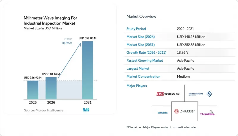
據 Mordor Intelligence 稱,用於工業檢測的毫米波成像市場預計將從 2025 年的 1.2692 億美元和 2026 年的 1.4813 億美元成長到 2031 年的 3.5288 億美元,2026 年至 2031 年的年複合成長率(CAGR)為 18.96%。
毫米波成像技術在工業檢測中的全球趨勢與洞察
無損在線品管的擴展
當批量抽樣無法達到「零缺陷」的預期時,線上無損檢測的重要性日益凸顯。毫米波系統具有非接觸、非電離的特性,並且能夠以輸送機的速度運行,從而實現100%的在線檢測。因此,對於需要在不中斷物料流動的情況下覆蓋檢測區域的工廠而言,毫米波成像在工業檢測市場中扮演著至關重要的角色。 2026年7月,羅德與施瓦茨公司發布了R&S IMAGER成像系統,該系統配備了可與現有生產管理軟體連接的標準介面。該系統使工程師能夠在不重新設計大型製造環境的情況下擴展體積檢測的範圍。 2025年IEEE Access的一項研究報告了航太和汽車零件中自動化近距離成孔徑雷達(SAR)缺陷定位的應用,並提供了一個以生產為中心的案例研究。
影像保存功能為線上檢測提供了實用的記錄保存優勢。每個毫米波影像都可以儲存為被檢物品的可追溯表示。此記錄支援品質審核和電子文件要求。這種方法不同於僅產生2D投影以即時做出合格/不合格判斷的檢測方法。 2024年,費迪南德·布勞恩實驗室推出了一款110 GHz線掃描器,配備80個單晶片整合檢測器,讀取速率高達每秒15,000幅影像。這表明,對於工業檢測市場中某些毫米波成像的線上應用而言,成像吞吐量並非主要限制因素。
越來越需要無需打開產品即可檢查密封包裝。
食品、製藥和物流企業需要在不打開包裝的情況下驗證其內容物。傳統的攝影機和稱重工具無法持續評估密封物品的內部狀況。毫米波訊號可以穿透常見的包裝材料,例如紙板、塑膠、複合薄膜和玻璃。這使得無需直接接觸即可檢查產品是否存在、密封缺陷以及零件是否缺失。據 ThruWave 公司稱,他們的平台可以以每分鐘 600 英尺(約每秒 4 個包裝盒)的速度檢測密封包裝盒。此應用案例進一步鞏固了毫米波成像技術在工業檢測市場包裝檢驗領域的地位。
ACM於2025年進行的一項研究調查了利用毫米波合成孔徑雷達成像技術檢測包裝穿透性液體洩漏的方法。研究報告稱,該方法在洩漏檢測和液體識別方面的準確率超過93%,比評估的基準方法高出14.70%。這種檢測方法解決了視覺系統無法穿透包裝材料進行內部觀察的難題。羅德與施瓦茨公司也發現,其系統能夠檢測密封玻璃瓶中的真空洩漏,而X光檢測無法可靠地識別此類缺陷。這項技術拓展了毫米波成像技術的應用範圍,使其不再局限於異物檢測,而是可以用於包裝的物理檢驗。
高昂的系統和整合成本
一套完整的檢測單元需要多通道收發器陣列、訊號處理系統、人工智慧分析軟體以及與生產線的機械整合。對於中小型製造商而言,這筆資本投入可能難以負擔。工作頻率在 95 GHz 至 300 GHz 範圍內的系統依賴專用化合物半導體製程和高精度波導元件。這些元件的成本通常高於基於通用 CMOS 感測器的光學相機系統。此外,用於工業檢測市場的毫米波成像還需要整合工作,將掃描器的輸出連接到製造執行系統和生產管理軟體。這項工作可能需要對檢測單元進行重新檢驗。
ThruWave於2025年8月完成了與Maple Systems cMT3000系列人機介面的整合。此次部署支援多PLC通訊和可配置介面,充分滿足了不同生產環境的實際需求。因此,在價格敏感型環境中,現有的X光系統仍具有優勢。 Qorvo和Sivers Semiconductors的晶片級整合正在縮小部分成本差距。然而,僅靠硬體成本的降低無法抵消軟體整合、生產線安裝和製程驗證的成本。即使檢測能力在技術上已具備,這些因素也可能導致部署延遲。
細分市場分析
到2025年,主動式毫米波成像系統將佔據工業檢測領域毫米波成像市場82.47%的佔有率。這些系統內建的照明光源可在生產環境中提供一致的影像對比度,這在生產過程中環境溫度波動的情況下尤其重要。製藥、食品和電子產品製造商正在採用主動式方法,即使在高速運作條件下也能獲得可預測的影像品質。一致的成像還可以減少人工智慧分類前手動重新校準的需求。 R&S IMAGER採用專有的毫米波源穿透包裝材料,並透過感測器陣列重建表面下影像。其基於ISAR的體積重建技術支援用於輸出的數位孿生格式。這種主動式架構非常適合對覆蓋一致性要求極高的受控生產環境。
被動式毫米波成像系統預計到2031年將以19.23%的複合年成長率成長。物流業者可在環境熱對比度足以提供異常偵測資訊的情況下使用這些系統。被動式系統無需主動光源,適用於成本要求較高的應用情境。其影像品質更直接取決於目標產品與其周圍環境之間的熱對比。因此,在環境對比不明顯的情況下,其應用受到限制。 TeraSense公司致力於研發以矽為基礎的兆赫檢測器,將偵測和訊號處理整合在單一晶片上。這種方法可以降低硬體成本,同時縮小與主動式系統在影像品質上的差距。這將使毫米波成像技術在工業檢測市場中得到更廣泛、更經濟高效的應用。
到2025年,整合式線上檢測系統將佔據工業檢測領域毫米波成像市場38.73%的佔有率。食品、製藥和電子產品的OEM製造商正在將這些系統直接安裝在輸送機上。當製程流程穩定時,這種方法可以實現100%的吞吐量檢測。這適用於需要連續檢測預包裝產品和標準化零件的工廠。這種整合方式可以將影像與生產管理系統和下游加工決策關聯起來,還可以儲存影像記錄以供後續品質審核。雖然這種組合有時需要專門的工程設計進行安裝,但它使線上系統成為目前最大的應用形式。在產品形狀和吞吐量適合輸送機運輸的工業檢測市場中,這種應用形式將繼續發揮核心作用。
預計到2031年,手持式和可攜式偵測系統將以19.44%的複合年成長率成長。在建築、基礎設施和物流領域,這些系統的應用場景通常發生在固定生產線之外。工程師可以使用可攜式掃描器來檢測水泥建築物、複合板和建築外觀。一項2026年的研究評估了毫米波在纖維板製造階段進行無損品質分析的應用,為現場部署提供了技術基礎。對於無法放置在輸送機上的航太和汽車零件,獨立系統仍然發揮著至關重要的作用。 2024年11月,FieldFox手持式分析儀系列的頻率範圍擴展至170 GHz,擴大了可攜式兆赫測量範圍,方便現場用戶使用。因此,其高度便攜性使得在零件尺寸和操作條件各異的現場進行檢測成為可能。
區域分析
預計到2025年,亞太地區將佔據毫米波成像工業檢測市場35.71%的佔有率,並將在2031年之前以19.74%的複合年成長率持續成長。中國電子組裝、食品加工和製藥業的契約製造設施正在推動該地區的需求。政府對品質基礎設施的投資也促進了自動化全流程檢測作為人工抽樣的替代方案。日本的汽車供應鏈遵循符合IATF 16949標準的「零缺陷」要求。這些要求正在推動電動車電池組件和電力電子產品的檢測。韓國DRAM和NAND快閃記憶體產能的擴張正在推動對基板缺陷篩檢的需求。當X光電腦斷層掃描(CT)需要大量運算資源時,使用毫米波探針的無損檢測可以成為切實可行的替代方案。
北美是毫米波成像工業檢測市場第二大區域。製藥、物流和航太領域的應用推動了全部區域的需求。總部位於西雅圖的ThruWave公司提供的服務無需使用電離輻射即可自動偵測郵件(例如小包裹、扁平郵件和信封)中的違禁物品。美國聯邦航空管理局(FAA)關於複合材料結構檢測的指導意見以及美國國防部的無損檢測標準正在促進美國製造群的航太相關活動。加拿大汽車產業走廊也提供了更多應用案例。墨西哥的電子組裝基地也為該地區的需求做出了貢獻。這些應用將產品完整性、包裝篩檢和複合材料檢測在北美地區連結起來。
歐洲的特點是擁有強大的工業測量能力和高標準的集中度。德國受益於羅德與施瓦茨公司及其大規模的汽車和資本財製造地。在法國,Teratonics SAS、Optikan SAS 和 MC2 Technologies SAS 等公司構成了一個正在蓬勃發展的測試設備叢集。英國的Faran Technologies 公司在波導元件方面擁有專業技術。南美洲的短期需求集中在巴西的食品加工和製藥業,出口合規性推動了對經過驗證的線上測試的需求。中東和非洲仍處於起步階段,但阿拉伯聯合大公國的產業多元化以及沙烏地阿拉伯的「2030願景」帶來了長期的機會。非洲的活動主要集中在研究機構和測試實驗室。
其他好處:
- Excel格式的市場預測(ME)表
- 3個月的分析師支持
目錄
第1章:引言
- 研究假設和市場定義
- 調查範圍
第2章:調查方法
第3章執行摘要
第4章 市場狀況
- 市場概覽
- 市場促進因素
- 無損在線品管的擴展
- 越來越需要無需打開產品即可檢查密封包裝。
- 對「零缺陷」和產品安全提出更嚴格的要求。
- 將基於人工智慧的缺陷識別與毫米波影像結合
- 高通量自動化生產線的擴建
- 複合材料和介電材料的多模態測試方法拓展
- 市場限制因素
- 高昂的系統和整合成本
- 它含有大量水分,但對高導電材料的滲透性有限。
- 校準的複雜性以及特定應用模型的學習。
- 毫米波工業檢測檢驗標準的差異
- 宏觀經濟因素對市場的影響
- 產業供應鏈分析
- 科技趨勢
- 監理情勢
- 波特五力分析
第5章 市場規模與成長預測
- 依產品類型
- 主動式毫米波成像系統
- 被動式毫米波成像系統
- 按系統格式
- 桌上型/實驗室測試系統
- 手持式和可攜式檢測系統
- 獨立式檢測系統
- 整合式線上檢測系統
- 按頻段
- 30-57 GHz
- 57 至小於 95 GHz
- 95~300 GHz
- 按最終用戶行業分類
- 食品/飲料
- 製藥
- 物流、郵政服務、電子商務
- 航太/國防
- 汽車和運輸業
- 電子和半導體
- 建材
- 一般製造業和消費品
- 研究機構和測試實驗室
- 其他終端用戶產業
- 按地區
- 北美洲
- 美國
- 加拿大
- 墨西哥
- 南美洲
- 巴西
- 阿根廷
- 其他南美國家
- 歐洲
- 德國
- 英國
- 法國
- 義大利
- 西班牙
- 其他歐洲國家
- 亞太地區
- 中國
- 日本
- 印度
- 韓國
- ASEAN
- 其他亞太國家
- 中東和非洲
- 中東
- 沙烏地阿拉伯
- 阿拉伯聯合大公國
- 土耳其
- 其他中東國家
- 非洲
- 南非
- 奈及利亞
- 其他非洲國家
- 中東
- 北美洲
第6章 競爭情勢
- 市場集中度
- 策略趨勢
- 市佔率分析
- 公司簡介
- Rohde & Schwarz GmbH & Co. KG
- ThruWave, Inc.
- Optikan SAS
- HUBNER GmbH & Co. KG
- TeraSense Group, Inc.
- Malcam Ltd.
- Teratonics SAS
- Lytid AS
- Heliotis AG
- Millimeter Wave Products, Inc.
- Farran Technology Limited
- Eravant, Inc.
- SAGE Millimeter, Inc.
- QuinStar Technology, Inc.
- Virginia Diodes, Inc.
- Sivers Semiconductors AB
- Vayyar Imaging Ltd.
- Qorvo, Inc.
- ACST GmbH
- RPG Radiometer Physics GmbH
- MC2 Technologies SAS
第7章 市場機會與未來展望
According to Mordor Intelligence, the millimeter-wave imaging for industrial inspection market size is projected to expand from USD 126.92 million in 2025 and USD 148.13 million in 2026 to USD 352.88 million by 2031, registering a CAGR of 18.96% between 2026 and 2031.
Global Millimeter-Wave Imaging For Industrial Inspection Market Trends and Insights
Increasing Adoption of Non-Destructive Inline Quality Control
Inline non-destructive testing has become more important where batch sampling cannot meet zero-defect expectations. Millimeter-wave systems support 100% inline inspection because they are contactless, non-ionizing, and can operate at conveyor speeds. This makes the millimeter-wave imaging for the industrial inspection market relevant to factories that need coverage without stopping material flow. Rohde and Schwarz introduced the R&S IMAGER in July 2026 with standard interfaces for connection to existing production-control software. The system allows engineers to extend volumetric inspection coverage without redesigning the wider manufacturing environment. A 2025 IEEE Access study reported automated near-field synthetic aperture radar defect localization across aerospace and automotive components, providing a production-focused reference point for this use.
Image retention adds a practical record-keeping benefit to inline inspection. Each millimeter-wave image can be retained as a traceable representation of the inspected item. That record can support quality reviews and electronic documentation obligations. The approach differs from inspection methods that only produce a 2D projection for an immediate pass-or-fail decision. The Ferdinand-Braun-Institut presented a 110 GHz line scanner in 2024 with 80 monolithically integrated detectors and readout speeds of up to 15,000 images per second. This demonstrated that imaging throughput need not be the main constraint for some inline applications in the millimeter-wave imaging for industrial inspection market.
Rising Need to Inspect Sealed Packages Without Product Opening
Food, pharmaceutical, and logistics operators need to verify packaged goods without opening them. Conventional cameras and weight-based tools cannot consistently assess the internal condition of a sealed item. Millimeter-wave signals can pass through cardboard, plastics, laminated films, and glass used in common packaging. They can support checks for product presence, seal defects, and missing components without direct contact. ThruWave states that its platform inspects sealed boxes at up to 600 feet per minute and 4 items per second. The operating case is strengthening the role of the millimeter-wave imaging for the industrial inspection market in package verification.
A 2025 ACM study examined through-package liquid leakage detection using millimeter-wave synthetic aperture radar imaging. The study reported accuracy above 93% for leakage detection and liquid identification, which was 14.70% higher than the baseline methods it evaluated. This type of inspection addresses a gap where visual systems cannot see through packaging materials. Rohde and Schwarz also identified vacuum loss in sealed glass bottles as a condition that its system can detect. X-ray inspection cannot reliably identify this type of failure. The capability extends the use of millimeter-wave imaging beyond foreign-body screening and toward package-physics verification.
High System and Integration Costs
A fully configured inspection cell requires multichannel transceiver arrays, signal processing, AI analytics software, and mechanical integration with the production line. This capital requirement can be difficult for small and mid-size manufacturers to justify. Systems operating from 95 GHz to 300 GHz rely on specialized compound semiconductor processes and precision waveguide components. Their component costs are structurally higher than those of optical camera systems based on commoditized CMOS sensors. The millimeter-wave imaging for the industrial inspection market also requires integration work to connect scanner outputs with manufacturing execution and production-control software. This work can require inspection-cell revalidation.
ThruWave completed an integration of Maple Systems' cMT3000 series human-machine interfaces in August 2025. The deployment supported multi-PLC communication and configurable interfaces, showing the practical effort needed in varied production environments. Existing X-ray systems, therefore, retain an advantage in price-sensitive environments. Chip-level integration from Qorvo and Sivers Semiconductors is narrowing part of the cost difference. However, hardware savings do not eliminate the costs of software integration, line installation, and process validation. These considerations can delay adoption even where the inspection capability is technically suitable.
Other drivers and restraints analyzed in the detailed report include:
- Tightening Zero-Defect and Product-Safety Requirements
- Integration of AI-Based Defect Recognition With Millimeter-Wave Images
- Limited Penetration Through Water-Rich and Highly Conductive Materials
For complete list of drivers and restraints, kindly check the Table Of Contents.
Segment Analysis
Active millimeter-wave imaging systems held 82.47% of the millimeter-wave imaging for industrial inspection market share in 2025. Their built-in illumination source provides consistent image contrast on production floors. This is useful where ambient thermal conditions vary during a production run. Pharmaceutical, food, and electronics manufacturers use active designs for predictable image quality at operating speed. Consistent images can also reduce the need for manual recalibration before AI classification. The R&S IMAGER uses its own millimeter-wave source to transmit through packaging and reconstruct subsurface images through a sensor array. Its ISAR-based volumetric reconstruction supports the digital-twin format used in its output. This active architecture fits controlled production-floor environments where consistent coverage is important.
Passive millimeter-wave imaging systems are projected to expand at a CAGR of 19.23% through 2031. Logistics operators can use them where ambient thermal contrast provides enough information for anomaly detection. Passive systems avoid an active source and can suit situations with lower cost expectations. Their image quality depends more directly on the thermal contrast of the inspected product and its surroundings. This limits use where the environment does not provide clear contrast. TeraSense has described a move toward silicon-based sub-terahertz detector fabrication that would combine detection and signal processing on one chip. That approach can narrow the image-quality gap with active systems while reducing hardware cost. It supports a broader range of lower-cost inspection deployments in the millimeter-wave imaging for industrial inspection market.
Integrated inline inspection systems accounted for 38.73% of the millimeter-wave imaging market share for industrial inspection in 2025. Food, pharmaceutical, and electronics original equipment manufacturers install these systems directly on conveyor-based lines. The format supports 100% throughput inspection when the process flow is stable. It is suited to factories that need continuous coverage of packaged goods or standardized components. The integration can connect images to production control systems and downstream handling decisions. It can also retain image records for later quality review. This combination makes inline systems the largest format, even though installation can require specialized engineering. The format remains central to the millimeter-wave imaging for the industrial inspection market, where product geometry and throughput suit conveyance.
Handheld and portable inspection systems are projected to expand at a CAGR of 19.44% through 2031. Construction, infrastructure, and logistics use cases often occur outside a fixed production line. Engineers can use portable scanners for concrete structures, composite panels, and building facades. A 2026 study assessed millimeter waves for non-destructive quality analysis of fiber-based panels during production stages. This supports the technical basis for field deployment. Standalone systems retain a role for aerospace and automotive components that do not fit a conveyor. The November 2024 expansion of the FieldFox handheld analyzer series to 170 GHz increased portable sub-terahertz coverage for field users. Portability therefore extends inspection to sites with varying part sizes and access conditions.
Complete Report Scope:
- By Product Type
- Active Millimeter-Wave Imaging Systems
- Passive Millimeter-Wave Imaging Systems
- By System Format
- Benchtop/Laboratory Inspection Systems
- Handheld and Portable Inspection Systems
- Standalone Inspection Systems
- Integrated Inline Inspection Systems
- By Frequency Band
- 30 to less than 57 GHz
- 57 to less than 95 GHz
- 95 to 300 GHz
- By End-User Industry
- Food and Beverage
- Pharmaceutical
- Logistics, Postal and E-Commerce
- Aerospace and Defense
- Automotive and Transportation
- Electronics and Semiconductor
- Construction and Building Materials
- General Manufacturing and Consumer Goods
- Research Institutes and Testing Laboratories
- Other End-User Industries
- By Geography
- North America
- United States
- Canada
- Mexico
- South America
- Brazil
- Argentina
- Rest of South America
- Europe
- Germany
- United Kingdom
- France
- Italy
- Spain
- Rest of Europe
- Asia-Pacific
- China
- Japan
- India
- South Korea
- ASEAN
- Rest of Asia-Pacific
- Middle East and Africa
- Middle East
- Saudi Arabia
- United Arab Emirates
- Turkey
- Rest of the Middle East
- Africa
- South Africa
- Nigeria
- Rest of Africa
- Middle East
- North America
Geography Analysis
Asia-Pacific held 35.71% of the millimeter-wave imaging for industrial inspection market share in 2025 and is projected to expand at a CAGR of 19.74% through 2031. China's electronics assembly, food processing, and pharmaceutical contract manufacturing base supports regional demand. Government quality-infrastructure investment is also encouraging automated throughput inspection in place of visual sampling. Japan's automotive supply chains operate under zero-defect requirements linked to IATF 16949. These requirements support inspection of EV battery components and power electronics. South Korea's DRAM and NAND flash capacity expansion is increasing the need for substrate-defect screening. Millimeter-wave probe-based non-destructive testing can offer a practical alternative when X-ray computed tomography requires substantial computational resources.
North America is the second-largest regional area in the millimeter-wave imaging for industrial inspection market. Pharmaceutical, logistics, and aerospace applications support demand across the region. ThruWave operates from Seattle and provides automated mail contraband detection for parcels, flats, and envelopes without ionizing radiation. FAA guidance on composite structure inspection and US Department of Defense non-destructive evaluation standards support aerospace activity in US manufacturing clusters. Canada's automotive corridor provides additional use cases. Mexico's electronics assembly base also contributes to regional demand. These applications link product integrity, package screening, and composite inspection across North America.
Europe has strong industrial metrology capability and a high density of quality standards. Germany benefits from the presence of Rohde and Schwarz and a large automotive and capital-goods manufacturing base. France includes Teratonics SAS, Optikan SAS, and MC2 Technologies SAS in its developing inspection cluster. The United Kingdom contributes Farran Technology's waveguide component experience. South America's near-term demand centers on Brazil's food processing and pharmaceutical sectors, where export compliance supports interest in validated inline inspection. Middle East and Africa remains at an earlier stage, although industrial diversification in the United Arab Emirates and Saudi Arabia's Vision 2030 present longer-term opportunities. African activity is concentrated in research institutes and testing laboratories.
- Rohde & Schwarz GmbH & Co. KG
- ThruWave, Inc.
- Optikan SAS
- HUBNER GmbH & Co. KG
- TeraSense Group, Inc.
- Malcam Ltd.
- Teratonics SAS
- Lytid AS
- Heliotis AG
- Millimeter Wave Products, Inc.
- Farran Technology Limited
- Eravant, Inc.
- SAGE Millimeter, Inc.
- QuinStar Technology, Inc.
- Virginia Diodes, Inc.
- Sivers Semiconductors AB
- Vayyar Imaging Ltd.
- Qorvo, Inc.
- ACST GmbH
- RPG Radiometer Physics GmbH
- MC2 Technologies SAS
Additional Benefits:
- The market estimate (ME) sheet in Excel format
- 3 months of analyst support
TABLE OF CONTENTS
1 INTRODUCTION
- 1.1 Study Assumptions and Market Definition
- 1.2 Scope of the Study
2 RESEARCH METHODOLOGY
3 EXECUTIVE SUMMARY
4 MARKET LANDSCAPE
- 4.1 Market Overview
- 4.2 Market Drivers
- 4.2.1 Increasing Adoption of Non-Destructive Inline Quality Control
- 4.2.2 Rising Need to Inspect Sealed Packages Without Product Opening
- 4.2.3 Tightening Zero-Defect and Product-Safety Requirements
- 4.2.4 Integration of AI-Based Defect Recognition With mmWave Images
- 4.2.5 Growth of High-Throughput Automated Manufacturing Lines
- 4.2.6 Expansion of Multimodal Inspection for Composite and Dielectric Materials
- 4.3 Market Restraints
- 4.3.1 High System and Integration Costs
- 4.3.2 Limited Penetration Through Water-Rich and Highly Conductive Materials
- 4.3.3 Calibration Complexity and Application-Specific Model Training
- 4.3.4 Fragmented Standards for mmWave Industrial Inspection Validation
- 4.4 Impact of Macroeconomic Factors on the Market
- 4.5 Industry Supply-Chain Analysis
- 4.6 Technology Outlook
- 4.7 Regulatory Landscape
- 4.8 Porter's Five Forces Analysis
- 4.8.1 Threat of New Entrants
- 4.8.2 Bargaining Power of Suppliers
- 4.8.3 Bargaining Power of Buyers
- 4.8.4 Threat of Substitutes
- 4.8.5 Intensity of Competitive Rivalry
5 MARKET SIZE AND GROWTH FORECASTS (VALUE)
- 5.1 By Product Type
- 5.1.1 Active Millimeter-Wave Imaging Systems
- 5.1.2 Passive Millimeter-Wave Imaging Systems
- 5.2 By System Format
- 5.2.1 Benchtop/Laboratory Inspection Systems
- 5.2.2 Handheld and Portable Inspection Systems
- 5.2.3 Standalone Inspection Systems
- 5.2.4 Integrated Inline Inspection Systems
- 5.3 By Frequency Band
- 5.3.1 30 to less than 57 GHz
- 5.3.2 57 to less than 95 GHz
- 5.3.3 95 to 300 GHz
- 5.4 By End-User Industry
- 5.4.1 Food and Beverage
- 5.4.2 Pharmaceutical
- 5.4.3 Logistics, Postal and E-Commerce
- 5.4.4 Aerospace and Defense
- 5.4.5 Automotive and Transportation
- 5.4.6 Electronics and Semiconductor
- 5.4.7 Construction and Building Materials
- 5.4.8 General Manufacturing and Consumer Goods
- 5.4.9 Research Institutes and Testing Laboratories
- 5.4.10 Other End-User Industries
- 5.5 By Geography
- 5.5.1 North America
- 5.5.1.1 United States
- 5.5.1.2 Canada
- 5.5.1.3 Mexico
- 5.5.2 South America
- 5.5.2.1 Brazil
- 5.5.2.2 Argentina
- 5.5.2.3 Rest of South America
- 5.5.3 Europe
- 5.5.3.1 Germany
- 5.5.3.2 United Kingdom
- 5.5.3.3 France
- 5.5.3.4 Italy
- 5.5.3.5 Spain
- 5.5.3.6 Rest of Europe
- 5.5.4 Asia-Pacific
- 5.5.4.1 China
- 5.5.4.2 Japan
- 5.5.4.3 India
- 5.5.4.4 South Korea
- 5.5.4.5 ASEAN
- 5.5.4.6 Rest of Asia-Pacific
- 5.5.5 Middle East and Africa
- 5.5.5.1 Middle East
- 5.5.5.1.1 Saudi Arabia
- 5.5.5.1.2 United Arab Emirates
- 5.5.5.1.3 Turkey
- 5.5.5.1.4 Rest of the Middle East
- 5.5.5.2 Africa
- 5.5.5.2.1 South Africa
- 5.5.5.2.2 Nigeria
- 5.5.5.2.3 Rest of Africa
- 5.5.5.1 Middle East
- 5.5.1 North America
6 COMPETITIVE LANDSCAPE
- 6.1 Market Concentration
- 6.2 Strategic Moves
- 6.3 Market Share Analysis
- 6.4 Company Profiles (includes Global Level Overview, Market Level Overview, Core Segments, Financials as available, Strategic Information, Market Rank/Share, Products and Services, Recent Developments)
- 6.4.1 Rohde & Schwarz GmbH & Co. KG
- 6.4.2 ThruWave, Inc.
- 6.4.3 Optikan SAS
- 6.4.4 HUBNER GmbH & Co. KG
- 6.4.5 TeraSense Group, Inc.
- 6.4.6 Malcam Ltd.
- 6.4.7 Teratonics SAS
- 6.4.8 Lytid AS
- 6.4.9 Heliotis AG
- 6.4.10 Millimeter Wave Products, Inc.
- 6.4.11 Farran Technology Limited
- 6.4.12 Eravant, Inc.
- 6.4.13 SAGE Millimeter, Inc.
- 6.4.14 QuinStar Technology, Inc.
- 6.4.15 Virginia Diodes, Inc.
- 6.4.16 Sivers Semiconductors AB
- 6.4.17 Vayyar Imaging Ltd.
- 6.4.18 Qorvo, Inc.
- 6.4.19 ACST GmbH
- 6.4.20 RPG Radiometer Physics GmbH
- 6.4.21 MC2 Technologies SAS
7 MARKET OPPORTUNITIES AND FUTURE OUTLOOK
- 7.1 White-Space and Unmet-Need Assessment

 全球線上攝影檢測市場規模、佔有率、趨勢和成長分析報告(2026-2034年)
 1/4吋黑霧過濾器市場:全球市場預測,2026-2032年1/8吋黑霧過濾器市場:全球市場預測,2026-2032年相機鏡頭圓形偏光濾鏡市場:全球市場預測,2026-2032年
 機器視覺相機:市場佔有率分析、產業趨勢與統計、成長預測(2026-2031)
 線上攝影檢測市場機會、成長要素、產業趨勢分析及2026-2035年預測望遠鏡鏡頭濾鏡市場:依濾鏡類型、通路、最終用戶、相機類型、材料、鏡頭尺寸分類,全球預測(2026-2032年)卡扣式過濾器市場:按過濾器類型、過濾效率、技術、材料、最終用途和分銷管道分類,全球預測,2026-2032年相機以白色柔光濾鏡市場:按產品類型、分銷管道、價格範圍、應用和最終用戶分類 - 全球預測,2026-2032年
 偵測攝影系統市場分析及預測(至2035年):依類型、產品、服務、技術、組件、應用、最終用戶、功能、安裝類型及解決方案分類