


 |
市場調查報告書
商品編碼
2125753
自動化光學檢測設備:市場佔有率分析、產業趨勢與統計、成長預測(2026-2031)Automated Optical Inspection Equipment - Market Share Analysis, Industry Trends & Statistics, Growth Forecasts (2026 - 2031) |
||||||

※ 本網頁內容可能與最新版本有所差異。詳細情況請與我們聯繫。
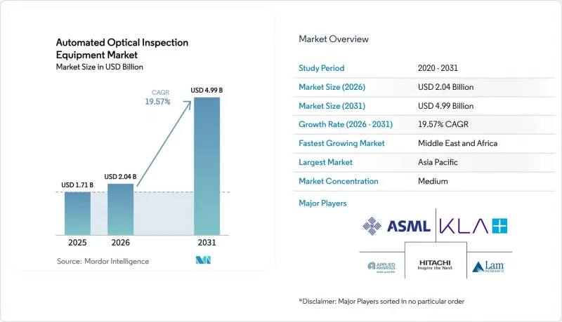
據 Mordor Intelligence 稱,2025 年自動光學檢測設備市值為 17.1 億美元,預計到 2031 年將達到 49.9 億美元,而 2026 年為 20.4 億美元,預測期(2026-2031 年)的複合年成長率為 19.57%。
本報告按產品類型(2DAOI系統、3DAOI系統)、技術(線上系統、離線/桌面系統)、組件(硬體、軟體/AI演算法)、終端用戶產業(半導體製造、PCB和EMS供應商、消費性電子組裝、其他)以及地區進行細分。市場預測以美元(USD)為單位。
全球自動化光學檢測設備市場趨勢及洞察
對高密度、小型化印刷電路板的需求日益成長
元件封裝尺寸已從 0402 封裝縮小到 0201 封裝,如今又正朝著 01005 封裝發展,這就要求在保持相同生產週期的同時,檢測解析度必須小於 10微米。 TRI 的 TR7700Q SII 平台透過引入同步多攝影機 3D 成像技術,實現了 1微米的解析度,可對動力傳動系統PCB 進行零缺陷檢測。汽車製造商正在採用此類技術來保護電池管理組件,而特斯拉針對安全關鍵基板的下一代 AOI 認證便證明了這一點。同樣,醫療植入製造商也要求檢測範圍小於 10微米,以確保產品核可;而 5G 無線基板需要無空隙的焊料填充,以確保毫米波訊號的完整性。這些需求的匯聚正在加速一級和二級 EMS 廠商用高精度 3D 平台取代傳統的 2D 偵測設備。
從2D到真正的3D偵測能力的過渡
傳統的2D系統無法量化BGA和晶片級封裝下方的共面性或焊球體積,這可能導致現場服務中出現缺陷。歐姆龍的VT-S1080採用多方向、多色照明,可將設定時間縮短70%,同時將體積精度提升至半導體等級。 KLA正在將這一理念擴展到先進封裝領域,並計劃將其2025年第二季30.8億美元的營收的一部分用於3D測量技術的研發,以解決晶片橋接和穿透矽通孔(TSV)中的空隙問題。線上3D回饋可實現鋼網自動清洗和焊膏塗覆校正,從而提高一次通過率並最大限度地減少下游製程的X光檢驗。隨著基板密度的增加,市場正持續轉型為3DAOI技術。
線上3D AOI技術具有高昂的資本投入和整合複雜性。
線上3D列印工作站每條生產線的成本在50萬至200萬美元之間,需要高精度輸送機、環境隔離以及與製造執行系統(MES)的整合。根據IPC的一項調查,隨著半導體短缺的持續,90%的基板製造商面臨平均14.5%的投入成本成長,導致資本投資空間有限。因此,規模小規模的EMS製造商推遲了設備升級,轉而依賴無法處理大批量、多品種生產線的離線桌面設備,導致採用率持續兩極化。此外,系統整合需要熟練的技術人員和備件,導致總擁有成本超出最初的預期。這可能會使小批量製造商的投資回收期延長三年以上。
細分市場分析
預計到2025年,3D平台將佔銷售額的56.72%,反映了自動化光學檢測設備市場向線速體積測量方向的轉變。半導體和汽車行業的客戶對共面性檢驗和焊膏高度分析的需求不斷成長,而這些功能是2D設備無法提供的,因此3D平台的市場佔有率有所上升。受晶片組件焊盤間距縮小的推動,預計到2031年,由3D系統驅動的自動化光學檢測設備市場規模將以13.86%的複合年成長率成長。 2D系統在消費性電子領域仍將發揮重要作用,尤其是在追求極致產能的契約製造工廠中,因為表面刮痕和極性檢測就足以滿足需求。
隨著感測器價格下降和演算法庫的日益成熟,2D 和 3D 之間的成本差距正在縮小。弗勞恩霍夫研究所的 SURFinpro 原型機證明,人工智慧可以用更少的攝影機重建焊點形狀,在降低元件成本的同時,達到接近 3D 的精度。因此,即使對於那些起初未能及時採用這項技術的電子製造服務 (EMS) 公司而言,投資回報率也得到了提升,從而加速了傳統 2D 生產線的淘汰。此外,製程分析已將焊膏體積測量與鋼網清洗週期連結起來,為企業提供可操作的數據,以減少廢品和保固退貨。
預計到2025年,線上檢測設備將佔據62.75%的市場佔有率,其封閉回路型回饋功能可在下游組裝流程之前隔離缺陷。隨著工業4.0先導計畫逐步推廣至全廠部署,自動化光學檢測設備市場中線上檢測設備的出貨量預計將以11.74%的複合年成長率成長。偵測框架內的邊緣伺服器支援模型本地運行,因此,貼上列印偏移無需操作員干預即可觸發印表機調整。
離線/桌面系統仍然用於小批量生產醫療和航太基板,這些基板需要在高倍率光學系統下進行長時間曝光。這些系統再次吸引了中小企業 (SME) 的關注,這些企業此前一直猶豫是否要投資與線上實施相關的資本支出 (CAPEX)。然而,隨著企業製造執行系統 (MES) 套件能夠捕捉 AOI 影像、預測模板磨損並匯出負責人認可的 Cpk 指標,線上系統的優勢得到了進一步提升。因此,北美、歐洲和亞太地區先進工廠的生產線設計人員現在已將線上 AOI 作為新建表面黏著技術線的標準規範。
區域分析
亞太地區預計在2025年繼續佔據56.65%的銷售額,主導中國對半導體製造設備490億美元的投資以及台積電在台灣的面板級封裝(PLP)項目。儘管亞太地區自動化光學檢測設備(AOI)的市場規模仍然龐大,但政策風險和薪資上漲促使一些原始設備製造商(OEM)將多元化經營至越南、印度和馬來西亞,導致新的AOI訂單分散全部區域。日本成熟的汽車電子產業則持續投資興建3D測量線,用於檢驗碳化矽(SiC)逆變器板上散熱器的共通性。
北美市場佔有率不斷擴大。這得歸功於《晶片製造和整合服務法案》(CHIPS Act)的津貼以及在地採購措施,這些措施使得晶圓廠能夠在國內採購線上檢測設備。預計到2027年,美國在晶片設備方面的資本投資將達到247億美元,自動線上偵測(AOI)的訂單積壓預計將保持強勁。然而,預計8萬名工程師的缺口可能導致勞動力短缺,並限制產能。墨西哥透過美墨加協定(USMCA)的連鎖效應獲得了電子製造服務(EMS)契約,作為回應,AOI供應商已在墨西哥新萊昂州開設服務中心,以支持近岸生產線。
歐洲正致力於技術獨立,將氣候政策資金用於節能型AOI模組,這些模組可降低20%的能耗。一家德國一級汽車零件供應商訂購了用於碳化矽功率模組的線掃描3D設備,而一家北歐新創公司則在其超級工廠引入了基於人工智慧的AOI技術,用於電池極耳的檢測。儘管英國脫歐使供應鏈複雜化並增加了海關手續,但荷蘭的本地庫存基地縮短了歐盟客戶的前置作業時間。
儘管中東和非洲的規模仍然相對較小,但預計其複合年成長率將達到13.92%,位居全球之首。這得益於各國政府推行產業多元化政策,並透過稅收優惠吸引PCB組裝和LED照明製造商。在沙烏地阿拉伯利雅德附近的電子製造走廊,首批入門級線上AOI(可檢測0201尺寸元件)訂單已經下達,這表明隨著技術能力的提升,未來將會有升級到3D檢測的訂單。
其他好處
- Excel格式的市場預測(ME)表
- 3個月的分析師支持
目錄
第1章:引言
- 研究假設和市場定義
- 調查範圍
第2章:調查方法
第3章執行摘要
第4章 市場狀況
- 市場概覽
- 市場促進因素
- 對高密度、小型化印刷電路基板。
- 從2D到真正的3D偵測能力的過渡
- 人工智慧驅動的自適應學習演算法的快速普及
- 新冠疫情後,北美和歐洲的電子製造業紛紛回流國內
- 基於邊緣運算的AOI可實現即時過程校正。
- 擴建吸頭和吸頭包裝線,需要進行小於 10微米。
- 市場限制因素
- 線上3D AOI技術面臨高資本支出(CAPEX)和整合複雜性等問題。
- 由於產品生命週期短,需要頻繁重新編程。
- 人工智慧資料標註領域AOI(自主資訊工程)人才供不應求
- 與成像感測器和雷射相關的貿易合規壁壘
- 宏觀經濟因素的影響
- 價值鏈分析
- 監理情勢
- 技術展望
- 生態系分析
- 波特五力分析
第5章 市場規模與成長預測
- 依產品類型
- 2DAOI系統
- 3D AOI系統
- 透過技術
- 線上系統
- 離線/桌面系統
- 按組件
- 硬體(攝影機、燈光、控制器)
- 軟體/人工智慧演算法
- 按最終用途行業分類
- 半導體製造
- PCB 和 EMS 供應商
- 家用電器組裝
- 汽車電子
- 太陽能電池和電池的製造
- 醫療器材
- 航太和國防電子
- 按地區
- 北美洲
- 美國
- 加拿大
- 墨西哥
- 南美洲
- 巴西
- 阿根廷
- 其他南美國家
- 歐洲
- 德國
- 英國
- 法國
- 義大利
- 俄羅斯
- 其他歐洲國家
- 亞太地區
- 中國
- 日本
- 韓國
- 印度
- ASEAN
- 其他亞太國家
- 中東和非洲
- 中東
- 沙烏地阿拉伯
- 阿拉伯聯合大公國
- 土耳其
- 其他中東國家
- 非洲
- 南非
- 奈及利亞
- 其他非洲國家
- 中東
- 北美洲
第6章 競爭情勢
- 市場集中度
- 策略趨勢
- 市佔率分析
- 公司簡介
- KLA Corporation
- Koh Young Technology Inc.
- Omron Corporation
- Saki Corporation
- Nordson Corporation(CyberOptics)
- Test Research, Inc.(TRI)
- Mirtec Co., Ltd.
- Viscom AG
- Camtek Ltd.
- Hitachi High-Tech Corporation
- Applied Materials, Inc.
- ASML Holding NV
- Lam Research Corporation
- JUTZE Intelligence Technology Co., Ltd.
- Goepel Electronic GmbH
- Mek(Marantz Electronics)
- Chroma ATE Inc.
- ViTrox Corp. Berhad
- PARMI Co., Ltd.
- Pemtron Corporation
- Orbotech(KLA)
- VI-Technology(Mycronic)
- Machine Vision Products, Inc.(MVP)
- ALeader Tech Co., Ltd.
- TechValley Co., Ltd.
第7章 市場機會與未來展望
According to Mordor Intelligence, the automated optical inspection equipment market size was valued at USD 1.71 billion in 2025 and estimated to grow from USD 2.04 billion in 2026 to reach USD 4.99 billion by 2031, at a CAGR of 19.57% during the forecast period (2026-2031).
This report is Segmented by Product Type (2D AOI Systems, 3D AOI Systems), Technology (Inline Systems, Offline/Desktop Systems), Component (Hardware, Software/AI Algorithms), End-Use Industry (Semiconductor Manufacturing, PCB and EMS Providers, Consumer Electronics Assembly, and More), and Geography. The Market Forecasts are Provided in Terms of Value (USD).
Global Automated Optical Inspection Equipment Market Trends and Insights
Increasing Demand for High-Density, Miniaturized PCBs
Component footprints shrank from 0402 to 0201 packages and are now moving toward 01005, forcing inspection resolutions below 10 µm while production takt times remain unchanged. TRI's TR7700Q SII platform demonstrated 1 µm resolution by deploying synchronized multi-camera 3D imaging for zero-escape inspection of power-train PCBs. Automakers adopted such capability to protect battery-management assemblies, as evidenced by Tesla's qualification of next-generation AOI on its safety-critical control boards. Medical-implant makers likewise mandated sub-10 µm coverage to secure product approvals, and 5G radio boards now require void-free solder volumes to assure mmWave signal integrity. These converging needs are accelerating replacement of legacy 2D stations with high-precision 3D platforms across both tier-one and tier-two EMS sites.
Transition from 2D to True-3D Inspection Capability
Legacy 2D systems cannot quantify coplanarity or solder-ball volume under BGAs and chip-scale packages, which leads to latent defects in field service. Omron's VT-S1080 adopted Multi-Direction Multi-Color illumination to reduce setup time by 70% while raising volumetric accuracy to semiconductor-grade thresholds. KLA extended the concept to advanced packaging, channeling a portion of its USD 3.08 billion Q2 FY 2025 revenue into 3D metrology R&D that addresses chiplet bridges and through-silicon via voids. Inline 3D feedback now triggers automatic stencil cleaning or solder-paste deposition correction, which increases first-pass yield and minimizes downstream X-ray verification. The market therefore continues to migrate toward 3D AOI as board densities climb.
High CAPEX and Integration Complexity of Inline 3D AOI
An inline 3D station costs USD 500,000-2 million per lane and demands precision conveyors, environmental isolation and MES interfacing. IPC surveys showed 90% of board houses contended with input-cost spikes averaging 14.5% as semiconductor shortages lingered, leaving limited headroom for capital purchases. Small EMS shops therefore postpone upgrades and rely on offline deskside units that cannot keep pace with high-mix high-volume lines, perpetuating a two-tier adoption pattern. Integration also requires trained technicians and spare parts, bringing total cost of ownership above initial quotations, which can delay ROI beyond three years for low-volume manufacturers.
Other drivers and restraints analyzed in the detailed report include:
- Rapid Adoption of AI-Enabled Adaptive Learning Algorithms
- Electronics Manufacturing Reshoring in North America and Europe
- Trade-Compliance Barriers on Imaging Sensors and Lasers
For complete list of drivers and restraints, kindly check the Table Of Contents.
Segment Analysis
3D platforms generated 56.72% of 2025 revenue, reflecting the automated optical inspection equipment market's pivot to volumetric measurement at line speeds. That share rose as semiconductor and automotive clients demanded co-planarity verification and paste-height analytics unavailable on 2D gear. The automated optical inspection equipment market size attributed to 3D systems is projected to climb at 13.86% CAGR through 2031, propelled by shrinking pad pitches in chiplet assemblies. 2D variants remain relevant for consumer electronics where surface-level scratch and polarity checks suffice, especially in contract factories pursuing extreme throughput.
The cost gap between 2D and 3D is narrowing as sensor prices fall and algorithm libraries mature. Fraunhofer's SURFinpro prototype proved that AI can reconstruct solder geometries with fewer cameras, trimming bill-of-material cost while approaching 3D accuracy. As a result, late-adopter EMS firms see improved ROI, which accelerates the retirement of legacy 2D lines. Because process analytics now tie paste-volume readings to stencil-cleaning cycles, operators gain actionable data that curtails scrap and warranty returns.
Inline machines secured 62.75% share in 2025 by providing closed-loop feedback that quarantines defects before downstream assembly. Inline shipments within the automated optical inspection equipment market are forecast to advance at 11.74% CAGR as Industry 4.0 pilots transition to plant-wide rollouts. Edge servers housed inside the inspection frame let models run locally so that paste-print offsets trigger printer adjustments without operator intervention.
Offline/desktop units continue to serve low-volume medical or aerospace boards requiring extended dwell time under high-magnification optics. These systems saw renewed interest among small businesses deterred by inline CAPEX. Yet the inline advantage has grown as enterprise MES suites now ingest AOI images to predict stencil wear and derive Cpk indicators that auditors accept. Consequently, line designers specify inline AOI as standard for new surface-mount tracks across North America, Europe and progressive APAC factories.
Complete Report Scope:
- By Product Type
- 2D AOI Systems
- 3D AOI Systems
- By Technology
- Inline Systems
- Offline / Desktop Systems
- By Component
- Hardware (Cameras, Illumination, Controllers)
- Software / AI Algorithms
- By End-use Industry
- Semiconductor Manufacturing
- PCB and EMS Providers
- Consumer Electronics Assembly
- Automotive Electronics
- Solar and Battery Manufacturing
- Medical Devices
- Aerospace and Defense Electronics
- By Geography
- North America
- United States
- Canada
- Mexico
- South America
- Brazil
- Argentina
- Rest of South America
- Europe
- Germany
- United Kingdom
- France
- Italy
- Russia
- Rest of Europe
- Asia-Pacific
- China
- Japan
- South Korea
- India
- ASEAN
- Rest of Asia-Pacific
- Middle East and Africa
- Middle East
- Saudi Arabia
- United Arab Emirates
- Turkey
- Rest of Middle East
- Africa
- South Africa
- Nigeria
- Rest of Africa
- Middle East
- North America
Geography Analysis
Asia-Pacific retained 56.65% of 2025 revenue on the strength of China's USD 49 billion semiconductor-equipment outlays and Taiwan's panel-level packaging projects led by TSMC. The automated optical inspection equipment market size attributed to Asia-Pacific remains substantial, yet policy risk and rising wages spurred some OEMs to diversify into Vietnam, India and Malaysia, dispersing new AOI orders across the region. Japan's mature automotive electronics base continued investing in 3D metrology lines that validate heat-sink coplanarity for SiC inverter boards.
North America's share expanded as CHIPS Act grants and local procurement policies drove fabs to source inline inspection domestically. Capital spending on US equipment is projected to reach USD 24.7 billion in 2027, ensuring steady AOI backlog, although an estimated 80,000 unfilled technician posts could constrain throughput if workforce.. Mexico captured spill-over EMS contracts under USMCA, prompting AOI vendors to open service centers in Nuevo Leon to support near-shoring lines.
Europe pursued technological self-reliance, channeling climate-policy funds toward energy-efficient AOI modules that cut power draw by 20%. Germany's Tier-1 auto suppliers ordered line-scan 3D units for silicon-carbide power modules, while Nordic start-ups adopted AI-based AOI for battery-cell tabs in gigafactories. Supply-chain complexity following Brexit added customs paperwork, but localized inventory pools in the Netherlands trimmed lead-times for EU customers.
Middle East and Africa, though still small, recorded the fastest 13.92% CAGR outlook as governments under industrial-diversification agendas lured PCB assemblers and LED lighting producers with tax incentives. Saudi Arabia's electronic-manufacturing corridor near Riyadh placed initial orders for entry-level inline AOI capable of 0201 inspection, signaling future upgrades to 3D as skill levels rise.
- KLA Corporation
- Koh Young Technology Inc.
- Omron Corporation
- Saki Corporation
- Nordson Corporation (CyberOptics)
- Test Research, Inc. (TRI)
- Mirtec Co., Ltd.
- Viscom AG
- Camtek Ltd.
- Hitachi High-Tech Corporation
- Applied Materials, Inc.
- ASML Holding N.V.
- Lam Research Corporation
- JUTZE Intelligence Technology Co., Ltd.
- Goepel Electronic GmbH
- Mek (Marantz Electronics)
- Chroma ATE Inc.
- ViTrox Corp. Berhad
- PARMI Co., Ltd.
- Pemtron Corporation
- Orbotech (KLA)
- VI-Technology (Mycronic)
- Machine Vision Products, Inc. (MVP)
- ALeader Tech Co., Ltd.
- TechValley Co., Ltd.
Additional Benefits:
- The market estimate (ME) sheet in Excel format
- 3 months of analyst support
TABLE OF CONTENTS
1 INTRODUCTION
- 1.1 Study Assumptions and Market Definition
- 1.2 Scope of the Study
2 RESEARCH METHODOLOGY
3 EXECUTIVE SUMMARY
4 MARKET LANDSCAPE
- 4.1 Market Overview
- 4.2 Market Drivers
- 4.2.1 Increasing demand for high-density, miniaturized PCBs
- 4.2.2 Transition from 2D to true-3D inspection capability
- 4.2.3 Rapid adoption of AI-enabled adaptive learning algorithms
- 4.2.4 Post-COVID reshoring of electronics manufacturing in North America and Europe
- 4.2.5 Edge-computing AOI for real-time process correction (under-the-radar)
- 4.2.6 Growth of chiplet and advanced-packaging lines needing sub-10 m inspection (under-the-radar)
- 4.3 Market Restraints
- 4.3.1 High CAPEX and integration complexity of inline 3D AOI
- 4.3.2 Short product lifecycles demanding frequent re-programming
- 4.3.3 Limited availability of AOI-talent for AI data-labelling (under-the-radar)
- 4.3.4 Trade-compliance barriers on imaging sensors and lasers (under-the-radar)
- 4.4 Impact of Macroeconomic Factors
- 4.5 Value Chain Analysis
- 4.6 Regulatory Landscape
- 4.7 Technological Outlook
- 4.8 Ecosystem Analysis
- 4.9 Porters Five Forces Analysis
- 4.9.1 Bargaining Power of Suppliers
- 4.9.2 Bargaining Power of Buyers
- 4.9.3 Threat of New Entrants
- 4.9.4 Threat of Substitutes
- 4.9.5 Intensity of Competitive Rivalry
5 MARKET SIZE AND GROWTH FORECASTS (VALUE)
- 5.1 By Product Type
- 5.1.1 2D AOI Systems
- 5.1.2 3D AOI Systems
- 5.2 By Technology
- 5.2.1 Inline Systems
- 5.2.2 Offline / Desktop Systems
- 5.3 By Component
- 5.3.1 Hardware (Cameras, Illumination, Controllers)
- 5.3.2 Software / AI Algorithms
- 5.4 By End-use Industry
- 5.4.1 Semiconductor Manufacturing
- 5.4.2 PCB and EMS Providers
- 5.4.3 Consumer Electronics Assembly
- 5.4.4 Automotive Electronics
- 5.4.5 Solar and Battery Manufacturing
- 5.4.6 Medical Devices
- 5.4.7 Aerospace and Defense Electronics
- 5.5 By Geography
- 5.5.1 North America
- 5.5.1.1 United States
- 5.5.1.2 Canada
- 5.5.1.3 Mexico
- 5.5.2 South America
- 5.5.2.1 Brazil
- 5.5.2.2 Argentina
- 5.5.2.3 Rest of South America
- 5.5.3 Europe
- 5.5.3.1 Germany
- 5.5.3.2 United Kingdom
- 5.5.3.3 France
- 5.5.3.4 Italy
- 5.5.3.5 Russia
- 5.5.3.6 Rest of Europe
- 5.5.4 Asia-Pacific
- 5.5.4.1 China
- 5.5.4.2 Japan
- 5.5.4.3 South Korea
- 5.5.4.4 India
- 5.5.4.5 ASEAN
- 5.5.4.6 Rest of Asia-Pacific
- 5.5.5 Middle East and Africa
- 5.5.5.1 Middle East
- 5.5.5.1.1 Saudi Arabia
- 5.5.5.1.2 United Arab Emirates
- 5.5.5.1.3 Turkey
- 5.5.5.1.4 Rest of Middle East
- 5.5.5.2 Africa
- 5.5.5.2.1 South Africa
- 5.5.5.2.2 Nigeria
- 5.5.5.2.3 Rest of Africa
- 5.5.5.1 Middle East
- 5.5.1 North America
6 COMPETITIVE LANDSCAPE
- 6.1 Market Concentration
- 6.2 Strategic Moves
- 6.3 Market Share Analysis
- 6.4 Company Profiles (includes Global level Overview, Market level overview, Core Segments, Financials as available, Strategic Information, Market Rank/Share, Products and Services, Recent Developments)
- 6.4.1 KLA Corporation
- 6.4.2 Koh Young Technology Inc.
- 6.4.3 Omron Corporation
- 6.4.4 Saki Corporation
- 6.4.5 Nordson Corporation (CyberOptics)
- 6.4.6 Test Research, Inc. (TRI)
- 6.4.7 Mirtec Co., Ltd.
- 6.4.8 Viscom AG
- 6.4.9 Camtek Ltd.
- 6.4.10 Hitachi High-Tech Corporation
- 6.4.11 Applied Materials, Inc.
- 6.4.12 ASML Holding N.V.
- 6.4.13 Lam Research Corporation
- 6.4.14 JUTZE Intelligence Technology Co., Ltd.
- 6.4.15 Goepel Electronic GmbH
- 6.4.16 Mek (Marantz Electronics)
- 6.4.17 Chroma ATE Inc.
- 6.4.18 ViTrox Corp. Berhad
- 6.4.19 PARMI Co., Ltd.
- 6.4.20 Pemtron Corporation
- 6.4.21 Orbotech (KLA)
- 6.4.22 VI-Technology (Mycronic)
- 6.4.23 Machine Vision Products, Inc. (MVP)
- 6.4.24 ALeader Tech Co., Ltd.
- 6.4.25 TechValley Co., Ltd.
7 MARKET OPPORTUNITIES AND FUTURE OUTLOOK
- 7.1 White-space and Unmet-need Assessment

 自主工業品質檢測市場預測至2034年-按產品、組件、部署模式、應用、最終用戶和地區分類的全球分析
 全球自動化光學檢測系統市場規模、佔有率、趨勢和成長分析報告(2026-2034年)人工智慧驅動的品管系統市場預測至2034年:按組件、檢測類型、技術、應用、最終用戶和地區分類的全球分析自主品質檢測系統市場預測至2034年-全球分析(按組件、檢測類型、技術、應用、最終用戶和地區分類)視覺引導檢測設備市場規模、佔有率、成長率、全球產業分析、區域趨勢及2026年至2034年預測。
 人工智慧(AI)AOI系統市場:按類型、技術、最終用戶、國家和地區分類-全球產業分析、市場規模、市場佔有率及2026年至2033年預測視覺引導檢測設備全球市場規模、佔有率、趨勢和成長分析報告(2026-2034年)
 自動化光學檢測市場-全球市場預測(2026-2032年)自動化光學檢測系統市場:2026-2032年全球市場預測(依產品、產品類型、平台、相機配置、應用、產業、組織規模及部署模式分類)
 人工智慧驅動的視覺檢測:市場佔有率分析、行業趨勢和統計數據、成長預測(2026-2031 年)