


 |
市場調查報告書
商品編碼
2124976
3D IC封裝:市場佔有率分析、產業趨勢與統計、成長預測(2026-2031年)3D IC Packaging - Market Share Analysis, Industry Trends & Statistics, Growth Forecasts (2026 - 2031) |
||||||

※ 本網頁內容可能與最新版本有所差異。詳細情況請與我們聯繫。
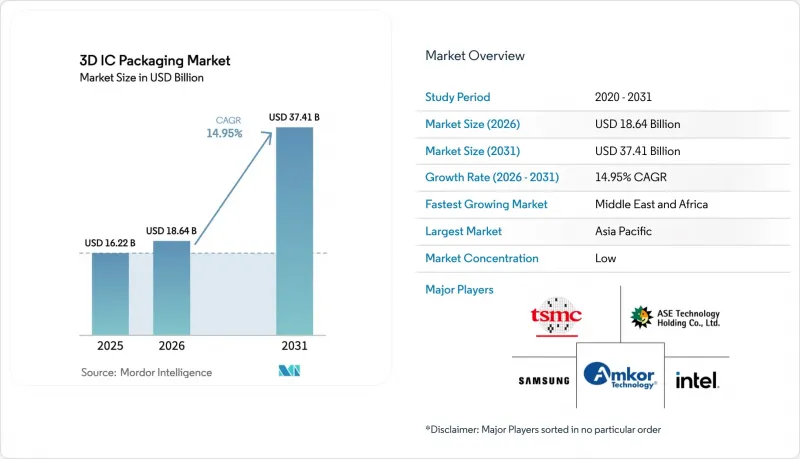
據 Mordor Intelligence 稱,3D IC封裝市場預計到 2026 年價值 186.4 億美元,高於 2025 年的 162.2 億美元,預計到 2031 年將達到 374.1 億美元。
預計 2026 年至 2031 年的複合年成長率為 14.95%。
本報告按封裝技術(3D TSV、3D WLCSP 等)、整合方式(2.5D 中介層、真 3D 堆疊等)、裝置類型(記憶體、邏輯/處理器等)、終端用戶應用(高效能運算與人工智慧、家用電子電器與行動裝置等)以及地區進行細分。市場預測以美元計價。
全球3D IC封裝市場趨勢與洞察
人工智慧/高效能運算領域對HBM堆疊封裝的需求呈爆炸性成長
資料中心加速器的浪潮正在重塑材料清單) 的優先級,而 3D IC封裝市場中的 HBM 堆疊技術已成為所有先進節點藍圖上的重中之重。台積電計劃在 2026 年將其 CoWoS 晶圓月產量提升至 88,000 片,以支援英偉達的下一代 GPU。從 HBM3E 到 HBM4+ 的過渡在保持熱設計限制的前提下,將有效頻寬密度提升了三倍,這迫使基板製造商對更厚的芯材和更精細的銅重分佈層進行認證。三星的 H-Cube 平台將邏輯和記憶體整合在封裝上,顯示以記憶體為中心的拓撲結構正在擴展到基板級架構。因此,每個裝置的堆疊晶片比例正在增加,TSV 配置變得更加多樣化,最終導致整個 3D IC封裝市場的平均售價 (ASP) 上漲。
行動和穿戴式裝置向晶圓級晶片封裝 (WLCSP) 的過渡
穿戴式裝置和高階智慧型手機製造商目前正將晶圓級系統級封裝 (WLCSP) 作為標準方法,用於在小於 7 毫米的平台上封裝無線模組、電源管理積體電路 (PMIC) 和微機電系統 (MEMS)。蘋果公司 2026 年的旗艦機型預計將在其 A 系列 SoC 中採用先進的 WLCSP 技術,這徵兆尺寸優勢正在超越傳統的「每引腳成本」權衡。為此,台灣的 OSAT 廠商正在將其用於 RDL 優先線路重布的光刻生產線數量翻倍,而韓國的競爭對手則轉向使用樹脂塗覆的銅箔來減少翹曲。這些發展正在將 3D IC封裝市場從資料中心晶片擴展到日常消費性電子設備,從而帶來多元化的收入來源和更高的晶圓廠運轉率。
TSV製造設備和CoWoS生產能力短缺
TSV蝕刻設備、鍵結對準器和CoWoS相容基板貼合機的訂單仍然訂單了12到18個月之後,這限制了OSAT(外包技術組裝和測試)公司的成長潛力,這些公司正面臨著滿足人工智慧加速器交付期限的壓力。應用材料公司和東京電子公司都預計,到2026年中期,設備訂單積壓將達到兩位數,但由於元件和安裝人員短缺,實際的產能擴張被推遲。由於台積電佔據了CoWoS基板的大部分佔有率,買家正在競相爭奪晶圓配額,有時甚至需要預付幾季的款項。即使有明顯的強勁需求徵兆,這種供不應求也阻礙了整個3D IC封裝市場即時獲利。
細分市場分析
2025年,3D TSV節點在3D IC封裝維持了37.96%的市佔率。這得益於成熟的光刻製程、量產設備以及與記憶體廠商每GB成本目標相符的現場可靠性數據。在多條HBM3E生產線上,TSV鑽孔和填充設備的攤銷已經完成,儘管晶片數量不斷增加,毛利率仍然保持穩定。同時,混合鍵結領域正以21.15%的複合年成長率快速成長,利用銅對銅直接接觸,將Z方向高度降低40%,互連電阻降低15%。這些電氣優勢對於高運算密度AI加速器至關重要,突破了傳統封裝基板逃逸佈線方式的限制。
這種轉變並不意味著TSV將會過時。相反,兩條發展路徑正在形成。 TSV仍將是大規模生產記憶體和感測器堆疊的標準技術,而混合鍵合技術將佔據3D IC封裝市場中運算密集、低延遲的細分領域。能夠在相鄰生產線上同時處理這兩種製程的OSAT(契約製造)可以獲得風險分散的訂單。隨著基板製造商擴大玻璃芯的生產規模,混合鍵合技術的對準精度也在進一步提高,這意味著未來兩種技術的成本曲線可能會相交,並可能出現混合鍵合技術取代TSV技術,用於某些大規模生產的SKU的過渡階段。
2.5D中介層利用過去十年來的良率提升,將矽中介層的缺陷率降低至0.1 dpm以下,預計2025年將佔銷售額的57.38%。中介層將前端節點選擇與後端組裝分離,使GPU廠商能夠將光罩尺寸的運算單元與來自上一代節點的I/O晶片一同交付,而無需重新設計整個堆疊。然而,真正的3D堆疊技術正以21.28%的複合年成長率成長,這主要得益於晶片延遲的降低,從而能夠將模型訓練時間縮短兩位數百分比。典型的應用場景包括垂直NAND快閃記憶體、靠近記憶體的計算透鏡以及封裝中的高Q值射頻濾波器。在這些場景中,Z軸方向的接近性比平面光罩更為重要。
早期可靠性問題,例如嵌入式微凸塊中的電遷移和晶片角落的熱機械剪切,正透過低模量底部填充材料和採用混合鍵合技術的銅擴散阻擋層來緩解。隨著微流體冷卻和石墨烯散熱片技術的成熟,真正的3D技術應用正在加速。因此,3D IC封裝市場正在分化為兩個領域:一個領域以中介層為主導,另一個領域則以採用真正層狀結構的高效能解決方案為主導,這兩個領域不僅在價格上不斷發展,而且在關鍵績效指標(KPI)藍圖上也存在差異。
區域分析
預計到2025年,亞太地區將佔據3D IC封裝市場62.41%的佔有率。這主要得益於台灣在先進製程節點上的主導地位、韓國以記憶體為中心的後端產業叢集以及中國當地擴大國內產能的努力。台積電的CoWoS、三星的H-Cube和日月光的FOCoS等平台支撐著密集的供應商生態系統,從而減少了物流延誤並加快了製程轉移週期。然而,地緣政治不利因素和轉移風險迫使一些客戶將採購來源轉向馬來西亞、新加坡和越南,雖然擴大了該地區的技術覆蓋範圍,但也略微增加了成本。
北美受惠於以美元計價的《晶片技術創新法案》(CHIPS Act),該法案為最先進的晶圓和先進封裝生產線的獎勵投資津貼。預計到2028年,台積電位於亞利桑那州的工廠和英特爾位於俄亥俄州的工廠的後端產能總合將超過每月10萬片晶圓,這將有助於抵禦來自亞洲的供應中斷。北美與英偉達、AMD以及眾多機器學習新創公司在地理位置上的接近性,強化了設計和製造之間的反饋循環,使其對3D IC封裝市場的發展方向擁有獨特的影響力,即便其絕對產量不如亞洲。
中東和非洲地區雖然規模較小,但預計複合年成長率最高,達19.06%。數十億美元的資金已投入阿拉伯聯合大公國政府支持的晶圓廠和沙烏地阿拉伯「2030願景」工業區的玻璃芯基板線和OSAT先導工廠。歐洲正致力於在汽車領域打造可靠性和綠色製造的領先地位,充分利用德國的電力電子技術和法國的光電叢集。拉丁美洲仍然是消費性電子產品的利基組裝中心,而東歐則專注於國防領域的安全封裝方案。這些發展共同促成了更廣泛的3D IC封裝市場中地域分散的生產能力和區域需求集群的形成。
其他好處:
- Excel格式的市場預測(ME)表
- 3個月的分析師支持
目錄
第1章 A
第2章:引言
- 研究假設和市場定義
- 調查範圍
第3章:調查方法
第4章執行摘要
第5章 市場狀況
- 市場概覽
- 市場促進因素
- 人工智慧/高效能運算 (HPC) 的爆炸性成長對 HBM 堆疊封裝的需求日益成長
- 行動和穿戴式裝置正在逐步過渡到晶圓級晶片封裝(WLCSP)。
- 晶圓代工——「晶圓代工 2.0」——一種整合封裝技術的策略(例如,台積電、三星)
- 玻璃芯材和麵板級基板可透過大規模生產降低成本。
- 安全的異質整合對於防禦型晶片至關重要。
- 優先採用低溫混合鍵結技術的碳中和半導體製造廠
- 市場限制因素
- TSV製造設備和CoWoS生產能力短缺
- 熱設計極限 (TDL) 超過 1 W/mm² 的挑戰
- 3D平面圖設計中較高的IP/EDA成本
- 初始 PLP 生產線的面板翹曲和產量降低超過 3%。
- 價值供應鏈分析
- 監理情勢
- 技術展望
- 五力分析
- 新進入者的威脅
- 買方的議價能力
- 供應商的議價能力
- 替代品的威脅
- 競爭公司之間的競爭
- 價格分析
第6章 市場規模及成長預測(價值,10億美元)
- 生產力
- 3D TSV
- 3D晶圓級晶片封裝(WLCSP)
- 混合鍵堆疊(WoW、CoW、SoIC)
- 扇出型 3D 和麵板級封裝 (PLP)
- 透過整合方法
- 2.5D 中介層
- 真正的3D堆疊
- 基於系統級封裝/晶片組的HI
- 依設備類型
- 記憶體(HBM、Wide-I/O、HMC)
- 邏輯/處理器
- 感測器和微機電系統
- 射頻和模擬
- 透過最終用戶應用程式
- 高效能運算和人工智慧
- 家用電子電器和行動裝置
- 汽車和高級駕駛輔助系統
- 航太/國防
- 醫療和工業IoT
- 地區
- 北美洲
- 美國
- 加拿大
- 墨西哥
- 歐洲
- 英國
- 德國
- 法國
- 義大利
- 其他歐洲國家
- 亞太地區
- 中國
- 日本
- 印度
- 韓國
- 其他亞洲國家
- 中東
- 以色列
- 沙烏地阿拉伯
- 阿拉伯聯合大公國
- 土耳其
- 其他中東國家
- 非洲
- 南非
- 埃及
- 其他非洲國家
- 南美洲
- 巴西
- 阿根廷
- 其他南美國家
- 北美洲
第7章 競爭情勢
- 市場集中度
- 策略趨勢
- 市佔率分析
- 公司簡介
- Taiwan Semiconductor Manufacturing Co. Ltd.
- Samsung Electronics Co., Ltd.
- Advanced Semiconductor Engineering Inc.
- Amkor Technology Inc.
- Intel Corporation
- Siliconware Precision Industries Co. Ltd.
- GlobalFoundries Inc.
- Invensas Corporation
- Powertech Technology Inc.
- United Microelectronics Corporation
- Jiangsu Changjiang Electronics Technology Co. Ltd.
- Tongfu Microelectronics Co. Ltd.
- STATS ChipPAC Pte Ltd.
- ChipMOS Technologies Inc.
- ASE Test Limited
- Kyocera Corporation
- Texas Instruments Incorporated
- Micron Technology Inc.
- SK hynix Inc.
- Lam Research Corporation
第8章 市場機會與未來展望
- 評估閒置頻段和未滿足的需求
According to Mordor Intelligence, 3D IC packaging market size in 2026 is estimated at USD 18.64 billion, growing from 2025 value of USD 16.22 billion with 2031 projections showing USD 37.41 billion, growing at 14.95% CAGR over 2026-2031.
This report is Segmented by Packaging Technology (3D TSV, 3D WLCSP and More), Integration Approach (2. 5D Interposer, True 3D Stacking, and More), Device Type (Memory, Logic/Processor and More), End-User Application (HPC & AI, Consumer Electronics & Mobile, and More), and Geography. The Market Forecasts are Provided in Terms of Value (USD).
Global 3D IC Packaging Market Trends and Insights
Explosive AI / HPC Demand for HBM-Stacked Packages
A wave of data-center accelerators is reshaping bill-of-materials priorities, pushing HBM stacks inside the 3D IC packaging market to the top of every advanced-node roadmap. TSMC is scaling CoWoS output to 88,000 wafers per month by 2026 to keep pace with Nvidia's next-generation GPUs. The shift from HBM3E to HBM4+ triples effective bandwidth density while holding thermal design limits steady, forcing substrate makers to qualify thicker core materials and finer copper redistribution layers. Samsung's H-Cube platform couples' logic and memory on-package, illustrating how memory-centric topologies are cascading down to board-level architecture. The net effect is a higher stacked-die ratio per device, a richer TSV mix and, ultimately, an elevated ASP across the 3D IC packaging market.
Mobile and Wearables Shift to Wafer-Level Chip-Scale Packages (WLCSP)
Wearable and premium-smartphone OEMs now view wafer-level system-in-package footprints as the default path to squeezing radios, PMICs and MEMS into sub-7 mm platforms. Apple's 2026 flagship is widely expected to showcase advanced WLCSP for its A-series SoC, a signal that form-factor is trumping traditional cost-per-pin trade-offs. Taiwanese OSATs have responded by doubling lithography lines dedicated to redistributed-layer-count (RDL)-first flows, while South Korean rivals pivot toward resin-coated copper foils to mitigate warpage. These moves expand the 3D IC packaging market beyond data-center silicon and into everyday consumer devices, diversifying revenue streams and improving fab loading factors.
Scarcity of Production TSV Tools and CoWoS Capacity
TSV etchers, bonding aligners and CoWoS-grade substrate laminators remain booked 12-18 months out, constraining upside for OSATs scrambling to meet AI accelerator schedules. Applied Materials and Tokyo Electron both forecast double-digit equipment backlog into mid-2026, yet component shortages and install-crew bottlenecks slow actual ramp-ups. With TSMC commanding the lion's share of CoWoS substrates, buyers compete for wafer-start allocations, sometimes pre-paying quarters in advance. The scarcity curtails immediate revenue realization across the 3D IC packaging market even when demand signals are unmistakably strong.
Other drivers and restraints analyzed in the detailed report include:
- Foundry "Foundry 2.0" Strategy Integrating Packaging
- Glass-Core and Panel-Level Substrates Lowering Cost at Scale
- Defense-Grade Chiplets Mandate Secure Heterogeneous Integration
- Thermal-Design-Limit (TDL) Challenges Beyond 1 W/mm2
For complete list of drivers and restraints, kindly check the Table Of Contents.
Segment Analysis
3D TSV nodes retained 37.96% of the 3D IC packaging market share in 2025 because mature lithographic rules, bulk production tooling and field reliability data aligned with memory vendors' cost-per-GB targets. Multiple HBM3E lines already amortized their TSV drill and fill equipment, stabilizing gross margins even as die counts increased. Yet the hybrid-bond segment is expanding at a 21.15% CAGR, levering copper-to-copper direct contact to cut z-height by 40% and interconnect resistance by 15%. These electrical gains are pivotal in compute-dense AI accelerators that push beyond traditional package-substrate escape routing limits.
The pivot does not render TSV obsolete. Instead, dual-path roadmaps emerge: TSV remains the default for high-volume memory and sensor stacks, while hybrid bonding occupies compute-centric, low-latency corners of the 3D IC packaging market. OSATs able to host both flows on adjacent lines secure risk-diversified bookings. As substrate makers scale glass cores, hy-brid bonding alignment accuracy improves further, hinting at future cross-over where cost curves intersect and hybrid bonding usurps TSV in certain volume SKUs.
2.5D interposers booked 57.38% revenue in 2025, capitalizing on a decade of yield learning that brought silicon-interposer defectivity to <0.1 dpm. Because interposers decouple front-end node choice from back-end assembly, GPU vendors ship reticle-sized compute tiles beside older-node I/O dies without redesigning the full stack. However, true 3D stacking logs a 21.28% CAGR, fuelled by die-to-die latency gains that can cut model-training time by double-digit percentages. Flagship use cases include vertical NAND, near-memory compute lenses and in-package high-Q RF filters-all scenarios where z-axis proximity beats planar reticulation.
Early reliability fears-electro-migration in buried micro-bumps and thermo-mechanical shear at die corners-are being mitigated by low-modulus under-fills and hybrid-bond copper diffusion barriers. As micro-fluidic cooling and graphene heat-spreaders mature, true 3D adoption accelerates. The 3D IC packaging market therefore bifurcates into an interposer mainstream and a true-stacked performance edge, each advancing on differentiated KPI roadmaps rather than price alone.
Complete Report Scope:
- By Packaging Technology
- 3D TSV
- 3D Wafer-Level Chip-Scale Package (WLCSP)
- Hybrid-Bond Stacking (WoW, CoW, SoIC)
- Fan-Out 3D & Panel-Level Packaging (PLP)
- By Integration Approach
- 2.5D Interposer
- True 3D Stacking
- System-in-Package / Chiplet-based HI
- By Device Type
- Memory (HBM, Wide-I/O, HMC)
- Logic / Processor
- Sensor & MEMS
- RF & Analog
- By End-User Application
- High-Performance Computing & AI
- Consumer Electronics & Mobile
- Automotive & ADAS
- Aerospace & Defence
- Medical & Industrial IoT
- Geography
- North America
- United States
- Canada
- Mexico
- Europe
- United Kingdom
- Germany
- France
- Italy
- Rest of Europe
- Asia-Pacific
- China
- Japan
- India
- South Korea
- Rest of Asia
- Middle East
- Israel
- Saudi Arabia
- United Arab Emirates
- Turkey
- Rest of Middle East
- Africa
- South Africa
- Egypt
- Rest of Africa
- South America
- Brazil
- Argentina
- Rest of South America
- North America
Geography Analysis
Asia-Pacific commanded 62.41% of the 3D IC packaging market in 2025, a consequence of Taiwan's advanced-node hegemony, South Korea's memory-centric back-end clusters and mainland China's sprint toward domestic capacity. TSMC's CoWoS, Samsung's H-Cube and ASE's FOCoS platforms anchor dense supplier habitats, driving low logistics latency and fast process transfer loops. Even so, relocation risk under geopolitical crosscurrents pushes some customers to dual source into Malaysia, Singapore and Vietnam, lengthening the region's technology reach while marginally raising cost baselines.
North America benefits from USD-denominated CHIPS Act incentives that subsidize capex for both leading-edge wafers and advanced packaging lines. TSMC Arizona and Intel Ohio collectively exceed a projected 100,000 wafers per month of back-end capacity by 2028, a cushion against Asia-bound supply disruption. Proximity to Nvidia, AMD and a host of machine-learning start-ups tightens design-manufacturing feedback loops, granting North America disproportionate influence over the direction of the 3D IC packaging market even if absolute volume lags Asia.
The Middle East and Africa region posts the highest forecast CAGR at 19.06%, albeit from a small base. Sovereign-wealth-fund-backed fabs in the UAE and Saudi Arabia's Vision 2030 industrial zones earmark billions for glass-core substrate lines and OSAT pilot plants. Europe focuses on automotive reliability and green-manufacturing leadership, leveraging German power-electronic expertise and French photonics clusters. Latin America remains a niche assembly point for consumer devices, while Eastern Europe eyes defense-oriented secure-package initiatives. Together, these moves fragment capacity geographically, opening localized demand pockets inside the broader 3D IC packaging market.
- Taiwan Semiconductor Manufacturing Co. Ltd.
- Samsung Electronics Co., Ltd.
- Advanced Semiconductor Engineering Inc.
- Amkor Technology Inc.
- Intel Corporation
- Siliconware Precision Industries Co. Ltd.
- GlobalFoundries Inc.
- Invensas Corporation
- Powertech Technology Inc.
- United Microelectronics Corporation
- Jiangsu Changjiang Electronics Technology Co. Ltd.
- Tongfu Microelectronics Co. Ltd.
- STATS ChipPAC Pte Ltd.
- ChipMOS Technologies Inc.
- ASE Test Limited
- Kyocera Corporation
- Texas Instruments Incorporated
- Micron Technology Inc.
- SK hynix Inc.
- Lam Research Corporation
Additional Benefits:
- The market estimate (ME) sheet in Excel format
- 3 months of analyst support
TABLE OF CONTENTS
1 A
2 INTRODUCTION
- 2.1 Study Assumptions & Market Definition
- 2.2 Scope of the Study
3 RESEARCH METHODOLOGY
4 EXECUTIVE SUMMARY
5 MARKET LANDSCAPE
- 5.1 Market Overview
- 5.2 Market Drivers
- 5.2.1 Explosive AI / HPC demand for HBM-stacked packages
- 5.2.2 Mobile & wearables shift to Wafer-Level Chip-Scale Packages (WLCSP)
- 5.2.3 Foundry -Foundry 2.0- strategy integrating packaging (e.g., TSMC, Samsung)
- 5.2.4 Glass-core & panel-level substrates lowering cost at scale (under-the-radar)
- 5.2.5 Defense-grade chiplets mandate secure heterogeneous integration (under-the-radar)
- 5.2.6 Carbon-neutral fabs prioritising low-temperature hybrid bonding (under-the-radar)
- 5.3 Market Restraints
- 5.3.1 Scarcity of production TSV tools & CoWoS capacity
- 5.3.2 Thermal-design-limit (TDL) challenges beyond 1 W/mm-
- 5.3.3 High IP / EDA cost for 3D floor-planning (under-the-radar)
- 5.3.4 Panel warp & yield loss >3 % in early PLP lines (under-the-radar)
- 5.4 Value / Supply-Chain Analysis
- 5.5 Regulatory Landscape
- 5.6 Technological Outlook
- 5.7 Porter-s Five Forces
- 5.7.1 Threat of New Entrants
- 5.7.2 Bargaining Power of Buyers
- 5.7.3 Bargaining Power of Suppliers
- 5.7.4 Threat of Substitutes
- 5.7.5 Competitive Rivalry
- 5.8 Pricing Analysis
6 MARKET SIZE & GROWTH FORECASTS (VALUE, USD BN)
- 6.1 By Packaging Technology
- 6.1.1 3D TSV
- 6.1.2 3D Wafer-Level Chip-Scale Package (WLCSP)
- 6.1.3 Hybrid-Bond Stacking (WoW, CoW, SoIC)
- 6.1.4 Fan-Out 3D & Panel-Level Packaging (PLP)
- 6.2 By Integration Approach
- 6.2.1 2.5D Interposer
- 6.2.2 True 3D Stacking
- 6.2.3 System-in-Package / Chiplet-based HI
- 6.3 By Device Type
- 6.3.1 Memory (HBM, Wide-I/O, HMC)
- 6.3.2 Logic / Processor
- 6.3.3 Sensor & MEMS
- 6.3.4 RF & Analog
- 6.4 By End-User Application
- 6.4.1 High-Performance Computing & AI
- 6.4.2 Consumer Electronics & Mobile
- 6.4.3 Automotive & ADAS
- 6.4.4 Aerospace & Defence
- 6.4.5 Medical & Industrial IoT
- 6.5 Geography
- 6.5.1 North America
- 6.5.1.1 United States
- 6.5.1.2 Canada
- 6.5.1.3 Mexico
- 6.5.2 Europe
- 6.5.2.1 United Kingdom
- 6.5.2.2 Germany
- 6.5.2.3 France
- 6.5.2.4 Italy
- 6.5.2.5 Rest of Europe
- 6.5.3 Asia-Pacific
- 6.5.3.1 China
- 6.5.3.2 Japan
- 6.5.3.3 India
- 6.5.3.4 South Korea
- 6.5.3.5 Rest of Asia
- 6.5.4 Middle East
- 6.5.4.1 Israel
- 6.5.4.2 Saudi Arabia
- 6.5.4.3 United Arab Emirates
- 6.5.4.4 Turkey
- 6.5.4.5 Rest of Middle East
- 6.5.5 Africa
- 6.5.5.1 South Africa
- 6.5.5.2 Egypt
- 6.5.5.3 Rest of Africa
- 6.5.6 South America
- 6.5.6.1 Brazil
- 6.5.6.2 Argentina
- 6.5.6.3 Rest of South America
- 6.5.1 North America
7 COMPETITIVE LANDSCAPE
- 7.1 Market Concentration
- 7.2 Strategic Moves
- 7.3 Market Share Analysis
- 7.4 Company Profiles (includes Global level Overview, Market level overview, Core Segments, Financials as available, Strategic Information, Market Rank/Share for key companies, Products & Services, and Recent Developments)
- 7.4.1 Taiwan Semiconductor Manufacturing Co. Ltd.
- 7.4.2 Samsung Electronics Co., Ltd.
- 7.4.3 Advanced Semiconductor Engineering Inc.
- 7.4.4 Amkor Technology Inc.
- 7.4.5 Intel Corporation
- 7.4.6 Siliconware Precision Industries Co. Ltd.
- 7.4.7 GlobalFoundries Inc.
- 7.4.8 Invensas Corporation
- 7.4.9 Powertech Technology Inc.
- 7.4.10 United Microelectronics Corporation
- 7.4.11 Jiangsu Changjiang Electronics Technology Co. Ltd.
- 7.4.12 Tongfu Microelectronics Co. Ltd.
- 7.4.13 STATS ChipPAC Pte Ltd.
- 7.4.14 ChipMOS Technologies Inc.
- 7.4.15 ASE Test Limited
- 7.4.16 Kyocera Corporation
- 7.4.17 Texas Instruments Incorporated
- 7.4.18 Micron Technology Inc.
- 7.4.19 SK hynix Inc.
- 7.4.20 Lam Research Corporation
8 MARKET OPPORTUNITIES & FUTURE OUTLOOK
- 8.1 White-Space & Unmet-Need Assessment

 3D IC展望(2026):SOIC量產擴張,STCO崛起
 軟性電子產品材料市場規模、佔有率、成長、全球產業分析、區域趨勢及2026年至2034年預測
 半導體先進封裝市場報告:趨勢、預測與競爭分析(至2035年)
 先進積IC封裝市場-2026年至2032年全球市場預測
 2.5D 和 3D IC封裝市場預測至 2034 年—全球封裝技術、互連技術、材料、應用、最終用戶和區域分析3D IC 和 2.5D IC封裝市場:按封裝技術、組件、基礎設施和應用分類-2026-2032 年全球市場預測電源管理IC封裝市場:2026-2032年全球市場預測(依元件類型、封裝類型、封裝材料、佈線技術、應用與最終用途產業分類)
 3D IC 和 2.5D IC封裝市場規模、佔有率和成長分析:按封裝技術、應用、終端用戶產業和地區分類-2026-2033 年產業預測IC封裝市場預測至2034年-全球分析(整體封裝類型、互連技術、材料類型、晶圓尺寸、最終用途元件、服務類型、應用、經營模式和地區分類)軟性電子材料市場預測至2034年-按材料類型、組件、技術、應用和地區分類的全球分析