


 |
市場調查報告書
商品編碼
2124975
半導體前端設備:市場佔有率分析、產業趨勢與統計、成長預測(2026-2031)Semiconductor Front End Equipment - Market Share Analysis, Industry Trends & Statistics, Growth Forecasts (2026 - 2031) |
||||||

※ 本網頁內容可能與最新版本有所差異。詳細情況請與我們聯繫。
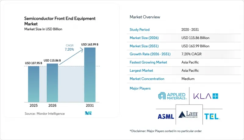
據 Mordor Intelligence 稱,2025 年半導體前端設備市場價值為 1079.5 億美元,預計到 2031 年將達到 1639.9 億美元,而 2026 年為 1158.6 億美元,預測期(2026-2031 年)複合年成長率為 7.2%。
本報告按設備類型(微影術、蝕刻、沉積和薄膜、其他)、終端用戶行業(代工和邏輯裝置、IDM、存儲器(DRAM 和 NAND)、特種模擬和電源裝置)、晶圓尺寸(300mm、200mm、150mm 和 100mm)、製程技術(5nm 及以上(5nm 及以下地區細分。市場預測以美元 (USD) 為單位。
全球半導體前端設備市場趨勢及洞察
人工智慧的進步正在加速向3奈米以下節點的過渡。
晶圓代工廠正在顯著加快其節點轉換週期,使奈米片製程的量產比傳統藍圖提前數年。台積電的N2製程、英特爾的18A生產線以及三星的2nm環柵(GAA)製程的量產都體現了這一快速進展,這些製程與領先的FinFET製程相比,蝕刻和沈積工序增加了約30%。這些額外的工序顯著增加了每條生產線所需的設備數量。此外,只有ASML能夠提供這些先進層所需的關鍵EUV光刻機。然而,ASML的產能有限,預計2026年其供應上限約為90台,這嚴重限制了其推出晶圓廠和有效擴大生產規模的能力。
HBM主導了對 TSV 和深矽蝕刻的需求激增。
受HBM3E封裝技術的進步推動(該技術可堆疊多達12個晶片),記憶體製造商對深反應離子蝕刻和銅填充沉積系統的訂單顯著成長。這種堆疊能力要求每片晶圓上擁有數萬個高長寬比孔,因此使用先進的製造設備至關重要。 Lam Research的「Flex」平台和Applied Materials的「Sym3 Y」腔室在該領域的訂單實現了兩位數的成長,凸顯了記憶體生產市場對這些技術日益成長的需求。
由於精密光學元件供應瓶頸,前置作業時間正在延長。
全球所有EUV光刻鏡片組件均由卡爾蔡司SMT獨家生產。其位於奧伯科亨的生產基地每年可為標準EUV系統生產40組鏡片組件,為高數值孔徑(NA)設備生產約10組鏡片組件。這種有限的產能造成了供應鏈的嚴重瓶頸,可能導致掃描器的前置作業時間長達30個月。此外,任何生產流程的中斷都可能嚴重影響生產進度,甚至可能使2奈米以下技術的量產啟動延遲長達18個月。有鑑於這些風險,ASML正積極與日本光學公司合作,推行雙供應商策略,以確保更穩健可靠的供應鏈。
細分市場分析
到2025年,在積極的晶圓代工和記憶體策略的支持下,微影術設備預計將佔銷售額的28.94%。這些設備在半導體製造過程中發揮著至關重要的作用,能夠實現先進晶片設計所需的精確圖形化。高數值孔徑(High-NA)極紫外光微影(EUV)平台,單價接近3.8億美元,預計將以11.72%的複合年成長率成長,從而推動與圖形化技術相關的半導體前端設備市場的發展。對這些平台日益成長的需求凸顯了它們在應對日益複雜的半導體裝置的重要性。其次,蝕刻系統佔了22%的市佔率。這主要得益於環柵(GaA)結構日益成長的重要性以及用於背面供電的等離子體製程的改進。這些系統對於實現現代晶片所需的複雜設計至關重要。沉積設備佔據了19%的市場佔有率,反映了原子層沉積(ALD)技術在高介電常數(高k)介質中的廣泛應用。原子層沉積(ALD)技術的日益普及反映了半導體產業轉向能夠提升元件性能和效率的材料和製程轉型。同時,儘管與套刻相關的預算有所減少,但檢測和測量領域的市佔率卻上升至12%。這一成長表明半導體製造對精確的品管和測量的需求日益成長。
離子布植、化學機械拋光 (CMP)、清洗、顯影劑和熱處理等傳統製程類別佔剩餘的 18% 支出。雖然這些製程類別已經成熟,但它們對整個半導體製造生態系統仍然至關重要。紮根於這些成熟領域的供應商面臨著來自迅速崛起的中國競爭對手的平均售價 (ASP) 壓力,這些競爭對手可以將價格壓低高達 25%。來自中國競爭對手的價格競爭對跨國供應商構成了重大挑戰。因此,全球供應商正在將其研發投資轉向盈利更高的產品和服務,例如極紫外光微影 (EUV)、矽通孔 (TSV) 和光化檢測。這種策略轉變旨在抓住高利潤機會,並在瞬息萬變的半導體市場中保持競爭優勢。
到2025年,台積電、三星晶圓代工和英特爾將引領晶圓代工和邏輯晶片製造市場,佔據總支出的46.21%。這些公司憑藉其先進的製造能力和對最尖端科技的巨額投資,一直保持著市場領先地位。同時,由SK海力士、三星和美光主導的記憶體領域預計將實現最快成長,複合年成長率(CAGR)將達到10.40%,這主要得益於HBM產能的擴張。記憶體領域的快速成長不僅推動了技術進步,也促進了半導體前端設備領域中TSV蝕刻、銅填充和晶圓鍵合技術設備的市場佔有率成長。這些設備對於高效能記憶體解決方案的生產至關重要。
隨著德州儀器和英飛凌加強其汽車模擬和功率晶片產品線,整合裝置製造商目前佔半導體產業支出的18%。這項轉變凸顯了汽車應用在半導體產業日益成長的重要性,尤其是在汽車越來越依賴複雜電子系統的情況下。同時,電動車對逆變器需求的激增也帶動了專業類比和功率晶片領域的客戶成長,佔據了剩餘的12%佔有率。這項需求表明,電動車在塑造半導體市場方面發揮著越來越重要的作用。關鍵設備領域的持續分化——邏輯裝置優先採用最先進的光刻技術,而記憶體則優先採用TSV和沈積技術——繼續影響供應商的策略。供應商正在調整其產品藍圖以應對這些不同的優先事項,並努力在快速變化的市場環境中保持競爭力。
區域分析
2025年,亞太地區繼續保持其主導地位,市佔率高達55.17%。這主要得益於台灣先進的半導體產業中心、韓國大規模的記憶體生產擴張以及印度積極建造補貼晶圓廠。光是台灣就佔全球半導體製造設備需求的約25%,並在其N2、N2P和A16生產線上對極紫外光刻和光學測量技術進行了大量投資。同時,韓國的資本投資重點在於推進HBM和2nm工藝,大量訂單集中在TSV、介質蝕刻和銅填充技術上,以增強產能。
北美則位居第二,佔全球市場佔有率的22%。關鍵項目對該地區的成長產生了顯著影響,包括英特爾在俄亥俄州、亞利桑那州和奧勒岡州的開發項目,德州儀器建立的300毫米模擬晶片生產線,以及格羅方德在馬耳他的擴張計劃。這些措施共同重塑了該地區的供應鏈,促使供應商紛紛建立本地製造地和服務中心。這項策略性舉措旨在利用《晶片和工業產品法案》(CHIPS Act)提供的激勵措施,進一步鞏固該地區在全球半導體市場的地位。
歐洲佔約12%的市場佔有率,其研發重點集中在特種模擬裝置、功率半導體以及高數值孔徑極紫外光刻(EUV)技術等領域的前沿舉措。意法半導體(STMicroelectronics)和英飛凌(Infineon)等公司致力於開發經濟高效且成熟的製程節點以保持競爭力,而imec和ASML之間的合作則推動了下一代光學測量解決方案的發展。南美洲以及中東和非洲地區目前在全球市場中所佔佔有率仍然較小,但沙烏地阿拉伯支持的各項舉措顯示該地區具有長期成長潛力。然而,要實現這一成長,需要解決該生態系統面臨的關鍵挑戰,包括培養技能型人才、確保水資源供應以及保障可靠的公共基礎設施。
其他好處
- Excel格式的市場預測(ME)表
- 3個月的分析師支持
目錄
第1章:引言
- 研究假設和市場定義
- 調查範圍
第2章:調查方法
第3章執行摘要
第4章 市場狀況
- 市場概覽
- 市場促進因素
- 人工智慧的進步正在加速向3奈米以下節點的過渡。
- 中國政府主導的大規模製造
- 5G和物聯網設備的復甦正在推動對成熟節點的需求。
- HBM主導了對 TSV 和深矽蝕刻的需求激增。
- 透過引入高數值孔徑極紫外技術,創造光度測量技術的需求。
- 印度待開發區300毫米晶圓廠(晶片連結)
- 市場限制因素
- 由於精密光學元件供應瓶頸,前置作業時間正在延長。
- 加強對先進微影術技術的出口限制
- 背面電源故障導致工具開發延誤的障礙。
- 強制性的淨零排放工廠要求推高了濕式工作台的總擁有成本 (TCO)。
- 產業價值鏈分析
- 監理情勢
- 技術展望
- 波特五力分析
第5章 市場規模與成長預測
- 依設備類型
- 微影術裝置
- 蝕刻設備
- 薄膜沉積和薄膜設備
- 離子布植裝置
- CMP設備
- 洗滌裝置
- 檢測和測量設備
- 塗層開發人員設備
- 熱處理設備
- 按最終用戶行業分類
- Foundry 和 Logic
- IDM(整合設備製造商)
- 記憶體(DRAM/NAND)
- 特殊模擬和電源
- 按晶圓尺寸
- 300mm
- 200mm
- 150毫米和100毫米
- 製程節點技術
- 5奈米或更小
- 6~16nm
- 28~65nm
- 超過 65 奈米(成熟)
- 按地區
- 北美洲
- 美國
- 加拿大
- 墨西哥
- 南美洲
- 巴西
- 阿根廷
- 其他南美國家
- 歐洲
- 德國
- 英國
- 法國
- 義大利
- 西班牙
- 其他歐洲國家
- 亞太地區
- 中國
- 日本
- 韓國
- 印度
- 澳洲
- 紐西蘭
- 其他亞太國家
- 中東和非洲
- 中東
- 阿拉伯聯合大公國
- 沙烏地阿拉伯
- 土耳其
- 其他中東國家
- 非洲
- 南非
- 奈及利亞
- 肯亞
- 其他非洲地區
- 中東
- 北美洲
第6章 競爭情勢
- 市場集中度
- 策略趨勢
- 市佔率分析
- 公司簡介
- Applied Materials Inc.
- KLA Corporation
- ASML Holding NV
- Lam Research Corporation
- Tokyo Electron Limited
- Nikon Corporation
- Canon Inc.
- SCREEN Holdings Co., Ltd.
- ASM International NV
- Advantest Corporation
- Disco Corporation
- Lasertec Corporation
- Axcelis Technologies Inc.
- Onto Innovation Inc.
- Veeco Instruments Inc.
- AMETEK Inc.
- Plasma-Therm LLC
- NAURA Technology Group Co., Ltd.
- Advanced Micro-Fab Equipment(AMEC)Inc.
- Shanghai Micro Electronics Equipment(SMEE)Co., Ltd.
- Ebara Corporation
- TEL Semes Co., Ltd.
- ULVAC Inc.
- ACCRETECH Inc.(Tokyo Seimitsu)
第7章 市場機會與未來展望
According to Mordor Intelligence, the semiconductor front-end equipment market size was valued at USD 107.95 billion in 2025 and estimated to grow from USD 115.86 billion in 2026 to reach USD 163.99 billion by 2031, at a CAGR of 7.2% during the forecast period (2026-2031).
This report is Segmented by Equipment Type (Lithography, Etch, Deposition and Thin-Film, and More), End-User Industry (Foundry and Logic, IDM, Memory DRAM and NAND, and Specialty Analog and Power), Wafer Size (300mm, 200mm, and 150mm and <=100mm), Process Node Technology (<=5nm, 6-16nm, 28-65nm, and >65nm Mature), and Geography. The Market Forecasts are Provided in Terms of Value (USD).
Global Semiconductor Front End Equipment Market Trends and Insights
AI-Accelerated Node Migration To Below 3 nm
Foundries are significantly accelerating their node-transition cycles, introducing nanosheet processes into production years ahead of their previously established roadmaps. This rapid advancement is evident in TSMC's N2 ramp, Intel's 18A line, and Samsung's 2 nm gate-all-around flow, all of which require approximately 30% more etch and deposition steps compared to their FinFET predecessors. These additional steps have led to a notable increase in the tool count per production line. Furthermore, only ASML has the capability to supply the essential EUV scanners required for these advanced layers. However, ASML's production capacity is limited, with a 2026 ceiling of approximately 90 units, which imposes significant constraints on fab start-ups and their ability to scale operations effectively.
HBM-Driven TSV And Deep-Silicon Etch Intensity Spike
Memory producers have significantly increased their orders for deep-reactive-ion etchers and copper-fill deposition tools, driven by the advancements in HBM3E packages, which now stack up to 12 dies. This stacking capability translates into tens of thousands of high-aspect-ratio vias per wafer, necessitating the use of advanced manufacturing tools. Both Lam Research's Flex platform and Applied Materials' Sym3 Y chamber have reported substantial double-digit order growth within this segment, highlighting the growing demand for these technologies in the memory production market.
Precision Optics Supply Bottlenecks Inflating Lead-Times
All EUV mirror sets globally are manufactured exclusively by Carl Zeiss SMT. The company's production facility in Oberkochen has the capacity to produce 40 assemblies annually for standard EUV systems and approximately 10 assemblies per year for High-NA tools. This limited production capacity results in scanner lead times that can extend up to 30 months, creating significant bottlenecks in the supply chain. Furthermore, any disruption in the production process could severely impact timelines, delaying the ramp-up of sub-2 nm technology by as much as 18 months. Recognizing these risks, ASML is actively pursuing dual sourcing strategies by collaborating with Japanese optics firms to ensure a more robust and reliable supply chain.
Other drivers and restraints analyzed in the detailed report include:
- Massive State-Backed Fab Build-Out In China
- High-NA EUV Roll-Out Spawning Actinic Metrology Demand
- Tightening Export Controls On Advanced Lithography
For complete list of drivers and restraints, kindly check the Table Of Contents.
Segment Analysis
In 2025, lithography tools accounted for 28.94% of the revenue, buoyed by assertive foundry and memory strategies. These tools play a critical role in the semiconductor manufacturing process, enabling precise patterning required for advanced chip designs. High-NA EUV platforms, each carrying a price tag close to USD 380 million, are set to expand at an 11.72% CAGR, propelling the semiconductor front-end equipment market tied to patterning technologies. The increasing demand for these platforms highlights their importance in meeting the growing complexity of semiconductor devices. Following closely, etch systems claimed a 22% share, driven by the rising prominence of gate-all-around structures and enhanced plasma steps for backside power delivery. These systems are essential for achieving the intricate designs required in modern chips. Deposition tools held a 19% stake, underscoring the growing adoption of ALD for high-k dielectrics. The wider use of ALD reflects the industry's shift towards materials and processes that enhance device performance and efficiency. Meanwhile, inspection and metrology climbed to a 12% share, even as overlay budgets tightened. This growth indicates the increasing need for precise quality control and measurement in semiconductor manufacturing.
Legacy categories, including ion implantation, CMP, cleaning, track-coat developers, and thermal processing, accounted for the remaining 18% of expenditures. These categories, while mature, remain vital to the overall semiconductor manufacturing ecosystem. Vendors entrenched in these established domains grapple with ASP pressures from swiftly advancing Chinese rivals, who can slash prices by as much as 25%. The competitive pricing from Chinese competitors poses significant challenges for multinational suppliers. As a result, global suppliers are redirecting R&D investments towards more lucrative offerings like EUV, TSV, and actinic inspection. This strategic shift aims to capitalize on higher-margin opportunities and maintain a competitive edge in the evolving semiconductor market.
In 2025, TSMC, Samsung Foundry, and Intel spearheaded the foundry and logic houses, accounting for 46.21% of the total expenditure. These companies have consistently led the market due to their advanced manufacturing capabilities and significant investments in cutting-edge technologies. Meanwhile, the memory segment, dominated by SK Hynix, Samsung, and Micron, is poised for the swiftest growth at a 10.40% CAGR, buoyed by HBM capacity expansions. This rapid growth in the memory sector is not only driving advancements in technology but also bolstering the market share of TSV etch, copper fill, and wafer-bonding tools in the semiconductor front-end equipment arena. These tools are critical for enabling the production of high-performance memory solutions.
Texas Instruments and Infineon, pivoting their lines for automotive analog and power chips, propelled integrated device manufacturers to capture 18% of the expenditures. This shift highlights the growing importance of automotive applications in the semiconductor industry, particularly as vehicles become increasingly reliant on advanced electronic systems. Meanwhile, a surge in demand for electric-vehicle inverters bolstered specialty analog and power customers, who claimed the remaining 12%. This demand underscores the expanding role of electric vehicles in shaping the semiconductor market. The ongoing divergence in equipment focus, prioritizing leading-edge lithography for logic and TSV and deposition for memory, continues to influence supplier strategies. Suppliers are adapting their roadmaps to address these distinct priorities, ensuring they remain competitive in a rapidly evolving market landscape.
Complete Report Scope:
- By Equipment Type
- Lithography Equipment
- Etch Equipment
- Deposition and Thin-Film Equipment
- Ion Implantation Equipment
- CMP Equipment
- Cleaning Equipment
- Inspection and Metrology
- Track, Coater and Developer
- Thermal Processing
- By End-User Industry
- Foundry and Logic
- IDM, Integrated Device Manufacturer
- Memory, DRAM and NAND
- Specialty Analog and Power
- By Wafer Size
- 300 mm
- 200 mm
- 150 mm and = 100 mm
- By Process Node Technology
- = 5 nm
- 6-16 nm
- 28-65 nm
- > 65 nm (Mature)
- By Geography
- North America
- United States
- Canada
- Mexico
- South America
- Brazil
- Argentina
- Rest of South America
- Europe
- Germany
- United Kingdom
- France
- Italy
- Spain
- Rest of Europe
- Asia Pacific
- China
- Japan
- South Korea
- India
- Australia
- New Zealand
- Rest of Asia-Pacific
- Middle East and Africa
- Middle East
- United Arab Emirates
- Saudi Arabia
- Turkey
- Rest of Middle East
- Africa
- South Africa
- Nigeria
- Kenya
- Rest of Africa
- Middle East
- North America
Geography Analysis
In 2025, the Asia-Pacific region maintained its dominance with a substantial 55.17% market share, primarily driven by Taiwan's advanced semiconductor hubs, South Korea's significant memory expansions, and India's proactive establishment of subsidy-supported fabs. Taiwan alone accounted for approximately 25% of the global demand for semiconductor tools, with its N2, N2P, and A16 production lines making substantial investments in EUV lithography and actinic metrology technologies. Meanwhile, South Korea's capital expenditures were heavily focused on advancing HBM and 2 nm processes, channeling significant orders toward TSV, dielectric etch, and copper fill technologies to enhance production capabilities.
North America followed as the second-largest contributor, securing a 22% revenue share in the global market. The region's growth was significantly influenced by major projects such as Intel's developments in Ohio, Arizona, and Oregon, Texas Instruments' establishment of 300 mm analog production lines, and GlobalFoundries' expansion efforts in Malta. These initiatives have collectively reshaped the regional supply chain, prompting equipment vendors to respond by setting up local manufacturing modules and service hubs. This strategic move aims to capitalize on the incentives provided under the CHIPS Act, further strengthening the region's position in the global semiconductor market.
Europe held an approximate 12% market share, with its focus centered on specialty analogs, power semiconductor sectors, and pioneering research initiatives for High-NA EUV technologies. Companies like STMicroelectronics and Infineon emphasized the development of cost-efficient mature nodes to remain competitive, while collaborations between imec and ASML advanced next-generation actinic metrology solutions. Although South America, the Middle East, and Africa remained minor contributors to the global market, initiatives backed by Saudi Arabia indicate potential long-term growth. However, realizing this growth will depend on addressing critical ecosystem challenges, including the development of skilled labor, access to water resources, and the availability of reliable utilities.
- Applied Materials Inc.
- KLA Corporation
- ASML Holding N.V.
- Lam Research Corporation
- Tokyo Electron Limited
- Nikon Corporation
- Canon Inc.
- SCREEN Holdings Co., Ltd.
- ASM International N.V.
- Advantest Corporation
- Disco Corporation
- Lasertec Corporation
- Axcelis Technologies Inc.
- Onto Innovation Inc.
- Veeco Instruments Inc.
- AMETEK Inc.
- Plasma-Therm LLC
- NAURA Technology Group Co., Ltd.
- Advanced Micro-Fab Equipment (AMEC) Inc.
- Shanghai Micro Electronics Equipment (SMEE) Co., Ltd.
- Ebara Corporation
- TEL Semes Co., Ltd.
- ULVAC Inc.
- ACCRETECH Inc. (Tokyo Seimitsu)
Additional Benefits:
- The market estimate (ME) sheet in Excel format
- 3 months of analyst support
TABLE OF CONTENTS
1 INTRODUCTION
- 1.1 Study Assumptions and Market Definition
- 1.2 Scope of the Study
2 RESEARCH METHODOLOGY
3 EXECUTIVE SUMMARY
4 MARKET LANDSCAPE
- 4.1 Market Overview
- 4.2 Market Drivers
- 4.2.1 AI-Accelerated Node Migration to Below 3 nm
- 4.2.2 Massive State-Backed Fab Build-Out in China
- 4.2.3 5G and IoT Device Rebound Lifting Mature-Node Demand
- 4.2.4 HBM-Driven TSV and Deep-Silicon Etch Intensity Spike
- 4.2.5 High-NA EUV Roll-Out Spawning Actinic Metrology Demand
- 4.2.6 India's Greenfield 300 mm Fabs (CHIPS-Linked) 2026-29
- 4.3 Market Restraints
- 4.3.1 Precision Optics Supply Bottlenecks Inflating Lead-Times
- 4.3.2 Tightening Export Controls on Advanced Lithography
- 4.3.3 Back-Side Power-Delivery Defect Hurdles Delaying Tools
- 4.3.4 Net-Zero Fab Mandates Raising Wet-Bench TCO
- 4.4 Industry Value-Chain Analysis
- 4.5 Regulatory Landscape
- 4.6 Technological Outlook
- 4.7 Porter's Five Forces Analysis
- 4.7.1 Bargaining Power of Buyers
- 4.7.2 Bargaining Power of Suppliers
- 4.7.3 Threat of New Entrants
- 4.7.4 Threat of Substitutes
- 4.7.5 Competitive Rivalry
5 MARKET SIZE AND GROWTH FORECASTS (VALUE)
- 5.1 By Equipment Type
- 5.1.1 Lithography Equipment
- 5.1.2 Etch Equipment
- 5.1.3 Deposition and Thin-Film Equipment
- 5.1.4 Ion Implantation Equipment
- 5.1.5 CMP Equipment
- 5.1.6 Cleaning Equipment
- 5.1.7 Inspection and Metrology
- 5.1.8 Track, Coater and Developer
- 5.1.9 Thermal Processing
- 5.2 By End-User Industry
- 5.2.1 Foundry and Logic
- 5.2.2 IDM, Integrated Device Manufacturer
- 5.2.3 Memory, DRAM and NAND
- 5.2.4 Specialty Analog and Power
- 5.3 By Wafer Size
- 5.3.1 300 mm
- 5.3.2 200 mm
- 5.3.3 150 mm and = 100 mm
- 5.4 By Process Node Technology
- 5.4.1 = 5 nm
- 5.4.2 6-16 nm
- 5.4.3 28-65 nm
- 5.4.4 > 65 nm (Mature)
- 5.5 By Geography
- 5.5.1 North America
- 5.5.1.1 United States
- 5.5.1.2 Canada
- 5.5.1.3 Mexico
- 5.5.2 South America
- 5.5.2.1 Brazil
- 5.5.2.2 Argentina
- 5.5.2.3 Rest of South America
- 5.5.3 Europe
- 5.5.3.1 Germany
- 5.5.3.2 United Kingdom
- 5.5.3.3 France
- 5.5.3.4 Italy
- 5.5.3.5 Spain
- 5.5.3.6 Rest of Europe
- 5.5.4 Asia Pacific
- 5.5.4.1 China
- 5.5.4.2 Japan
- 5.5.4.3 South Korea
- 5.5.4.4 India
- 5.5.4.5 Australia
- 5.5.4.6 New Zealand
- 5.5.4.7 Rest of Asia-Pacific
- 5.5.5 Middle East and Africa
- 5.5.5.1 Middle East
- 5.5.5.1.1 United Arab Emirates
- 5.5.5.1.2 Saudi Arabia
- 5.5.5.1.3 Turkey
- 5.5.5.1.4 Rest of Middle East
- 5.5.5.2 Africa
- 5.5.5.2.1 South Africa
- 5.5.5.2.2 Nigeria
- 5.5.5.2.3 Kenya
- 5.5.5.2.4 Rest of Africa
- 5.5.5.1 Middle East
- 5.5.1 North America
6 COMPETITIVE LANDSCAPE
- 6.1 Market Concentration
- 6.2 Strategic Moves
- 6.3 Market Share Analysis
- 6.4 Company Profiles (includes Global Level Overview, Market Level Overview, Core Segments, Financials as available, Strategic Information, Market Rank/Share, Products and Services, Recent Developments)
- 6.4.1 Applied Materials Inc.
- 6.4.2 KLA Corporation
- 6.4.3 ASML Holding N.V.
- 6.4.4 Lam Research Corporation
- 6.4.5 Tokyo Electron Limited
- 6.4.6 Nikon Corporation
- 6.4.7 Canon Inc.
- 6.4.8 SCREEN Holdings Co., Ltd.
- 6.4.9 ASM International N.V.
- 6.4.10 Advantest Corporation
- 6.4.11 Disco Corporation
- 6.4.12 Lasertec Corporation
- 6.4.13 Axcelis Technologies Inc.
- 6.4.14 Onto Innovation Inc.
- 6.4.15 Veeco Instruments Inc.
- 6.4.16 AMETEK Inc.
- 6.4.17 Plasma-Therm LLC
- 6.4.18 NAURA Technology Group Co., Ltd.
- 6.4.19 Advanced Micro-Fab Equipment (AMEC) Inc.
- 6.4.20 Shanghai Micro Electronics Equipment (SMEE) Co., Ltd.
- 6.4.21 Ebara Corporation
- 6.4.22 TEL Semes Co., Ltd.
- 6.4.23 ULVAC Inc.
- 6.4.24 ACCRETECH Inc. (Tokyo Seimitsu)
7 MARKET OPPORTUNITIES AND FUTURE OUTLOOK
- 7.1 White-Space and Unmet-Need Assessment

 射頻前端模組:市場佔有率分析、產業趨勢與統計、成長預測(2026-2031)
 射頻前端模組市場報告:趨勢、預測與競爭分析(至2035年)
 全球射頻前端模組市場預測至2034年:依組件、頻段、連接技術、材料、應用、最終用戶及地區分類
 射頻前端模組市場規模、佔有率和成長分析:按組件配置、應用、最終用戶產業、分銷管道和地區分類-2026-2033年產業預測
 射頻前端市場規模、佔有率和成長分析:按組件、技術、應用和地區分類-2026-2033年產業預測
 射頻前端模組和組件專利監測
 射頻前端模組市場規模、佔有率、趨勢和預測:按組件、應用和地區分類,2026-2034年
 射頻前端模組市場:依模組類型、頻寬、材質、應用及通路分類-2026-2032年全球預測
 2026年全球射頻前端市場報告
 射頻前端模組市場規模、佔有率和趨勢分析報告:按類型、技術、應用、地區和細分市場預測(2026-2033 年)