


 |
市場調查報告書
商品編碼
2124091
化合物半導體:市場佔有率分析、產業趨勢與統計、成長預測(2026-2031)Compound Semiconductor - Market Share Analysis, Industry Trends & Statistics, Growth Forecasts (2026 - 2031) |
||||||

※ 本網頁內容可能與最新版本有所差異。詳細情況請與我們聯繫。
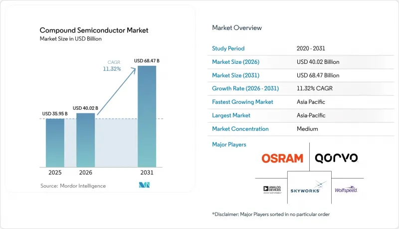
據 Mordor Intelligence 稱,化合物半導體市場預計到 2026 年價值 400.2 億美元,高於 2025 年的 359.5 億美元,預計到 2031 年將達到 684.7 億美元。
預計 2026 年至 2031 年的複合年成長率為 11.32%。
本報告材料類型(砷化鎵、氮化鎵、碳化矽等)、晶圓尺寸(100mm以下、150mm、200mm、300mm以上)、裝置類型(射頻和微波裝置等)、終端用戶產業(通訊和資料通訊基礎設施、家用電子電器、工業和能源等)以及中東地區工業和能源分類(北美、歐洲、亞太)以及中東地區。
全球化合物半導體市場趨勢及洞察
歐盟和中國電動車充電器中的氮化鎵矽基功率裝置
歐洲的排放氣體法規和中國的高速公路電氣化政策加速了350千瓦以上快速充電器中氮化鎵矽基(GaN-on-Si)技術的應用。這使得其功率轉換效率高達95%,與矽基替代方案相比,安裝成本降低了高達40%。歐盟綠色交易撥款20億歐元(約22.6億美元)用於寬頻隙半導體製造廠,進一步加速了這項轉型。同時,中國對鎵出口的限制也促進了在地採購策略的發展。
美國和亞太地區的 5G 大規模 MIMO 射頻前端
隨著向獨立組網5G和64T64R或更高規格天線陣列的過渡,需要使用GaAs和GaN功率放大器來降低基地台能耗40%並實現毫米波覆蓋。韓國的初步部署已涵蓋95%的人口,而藉助《晶片技術創新法案》(CHIPS Act)的津貼,美國晶圓廠已準備好擴大國內GaAs的生產規模。
200毫米碳化矽基板供不應求
由於晶錠生長週期長達14天且爐容量有限,製造商報告200毫米碳化矽晶片供不應求達40%。因此,汽車OEM廠商簽訂了多年期高價契約,使II-VI族等基板製造商擁有了定價權。
細分市場分析
在材料領域,砷化鎵在2025年仍維持化合物半導體市場46.85%的市佔率。碳化矽預計將以18.1%的複合年成長率成長,這主要得益於牽引逆變器和快速充電功率模組的應用。氮化鎵的市場佔有率也逐步提升,這主要得益於650V雙向積體電路的推出以及其在儲能雙向充電器中應用的不斷擴大。磷化銦雖然絕對體積較小,但仍是用於雷射雷達和亞太赫茲6G原型機的光子積體電路的關鍵材料。
各細分市場的成長主要得益於其寬頻寬間隙特性、高電子遷移率和高介電擊穿電壓,而這些特性是矽材料無法實現的。人們預期,GaN-on-Si在射頻應用領域的研究進展將拓展GaN的應用範圍,使其能夠應用於6G基地台的功率放大器。由於鎵和銦原料的出口限制持續存在,成本壓力仍然存在,這導致人們對回收材料和替代材料(例如Alyn)的興趣日益濃厚。
預計到2025年,150毫米基板將佔銷售額的48.02%,而200毫米平台預計將以14.95%的複合年成長率(CAGR)實現最高成長。 200毫米規格因其晶片數量要求高,更受汽車功率模組的青睞,預計與150毫米生產線相比,可將每片晶圓的晶圓成本降低30%。英飛凌位於馬來西亞的巨型晶圓廠憑藉其200毫米碳化矽(SiC)生產線展現了規模經濟效益,該生產線旨在到2030年滿足全球30%的供應量。
較小尺寸(100毫米以下)的設備在產量要求不高但性能至關重要的領域,例如衛星通訊,仍佔據重要地位。同時,儘管300毫米氮化鎵矽基原型機展現出商業機遇,但由於薄膜應力、翹曲控制和缺陷密度等技術挑戰,即使在預測期結束後,商業化仍未實現。設備供應商優先發展200毫米反應器平台,力求達到85-90%的運轉率,以最大限度地提高運轉率並攤銷資本投資成本。
區域分析
預計到2025年,亞太地區將佔全球銷售額的58.25%,到2031年,年複合成長率將達到13.95%。該地區的化合物半導體市場受益於中國計劃每月860萬片晶圓的產能以及台灣在晶圓代工行業的領先地位。然而,2024年實施的鎵、鍺和銦的出口限制凸顯了市場集中度風險,並促使地方政府為上游材料提供補貼。
在北美,390億美元的「晶片激勵計畫」(CHIPS 獎勵)加速了國內供應鏈的發展。 Skyworks和Covo計劃擴大砷化鎵(GaAs)的生產規模,台積電(TSMC)位於亞利桑那州的價值1650億美元的叢集也加快了建設,以整合用於化合物半導體的先進封裝能力。此外,國防部門為確保III-V族元件的安全供應而提出的要求也進一步推動了這項進程。
歐洲已將寬能隙半導體定位為其「綠色新政」和「歐洲晶片法案」的基石。德國已撥款20億歐元(約22.6億美元)用於國內生產,Nexperia公司也已投資2億美元在其位於漢堡的碳化矽生產線上進行建設。供應鏈本地化旨在減輕嚴重依賴亞洲的供應鏈所帶來的影響,例如北卡羅來納州石英礦的供應中斷曾威脅到全球70%至90%的超高純度石英的供應。
其他好處:
- Excel格式的市場預測(ME)表
- 3個月的分析師支持
目錄
第1章:引言
- 研究假設和市場定義
- 調查範圍
第2章:調查方法
第3章執行摘要
第4章 市場狀況
- 市場概覽
- 市場促進因素
- 歐盟和中國電動車充電器中的氮化鎵矽基功率裝置
- 美國和亞太地區的 5G 大規模 MIMO 射頻前端
- 微型/迷你LED在電視和AR穿戴裝置的應用
- 歐洲商用電動車用SiC牽引逆變器
- 美國和歐盟《晶片法案》對III-V族FABs的優惠待遇
- 用於自動駕駛車輛中基於 InP 的雷射雷達的 PIC 微控制器
- 市場限制因素
- 200毫米碳化矽基板供不應求
- MOCVD反應器的高額資本投入
- 氮化鎵裝置在650伏特以上電壓下的可靠性問題
- 美國對銷往中國的Epitol實施出口限制
- 價值鏈分析
- 技術展望
- 監理展望
- 波特五力分析
- 宏觀經濟趨勢對化合物半導體需求的影響
第5章 市場規模與成長預測
- 依材料類型
- 砷化鎵(GaAs)
- 氮化鎵(GaN)
- 碳化矽(SiC)
- 磷化銦(InP)
- 磷化鎵(GaP)
- 其他 III-V 族和 II-VI 族化合物
- 按晶圓尺寸
- 100毫米或更小
- 150 mm
- 200 mm
- 300毫米或以上
- 依設備類型
- 發光二極體(LED)
- 高頻和微波裝置
- 光電子學(雷射、檢測器)
- 電力電子
- 太陽能電池
- 按最終用戶行業分類
- 通訊和資料通訊基礎設施
- 家用電子產品
- 汽車和運輸業
- 工業和能源
- 航太/國防
- 醫療保健和生命科學
- 其他
- 按地區
- 北美洲
- 美國
- 加拿大
- 墨西哥
- 歐洲
- 德國
- 英國
- 法國
- 義大利
- 北歐國家(瑞典、芬蘭、挪威、丹麥)
- 其他歐洲國家
- 亞太地區
- 中國
- 日本
- 韓國
- 印度
- 台灣
- 其他亞太國家
- 南美洲
- 巴西
- 阿根廷
- 墨西哥
- 其他南美國家
- 中東和非洲
- 中東
- 沙烏地阿拉伯
- 阿拉伯聯合大公國
- 土耳其
- 其他中東國家
- 非洲
- 南非
- 其他非洲國家
- 中東
- 北美洲
第6章 競爭情勢
- 市場集中度
- 策略趨勢
- 市佔率分析
- 公司簡介
- Wolfspeed Inc.
- Skyworks Solutions Inc.
- Qorvo Inc.
- Infineon Technologies AG
- STMicroelectronics NV
- Onsemi(Semiconductor Components Industries LLC)
- Analog Devices Inc.
- Texas Instruments Inc.
- ams-OSRAM AG
- Rohm Semiconductor
- NXP Semiconductors NV
- GaN Systems Inc.
- Transphorm Inc.
- MACOM Technology Solutions Holdings Inc.
- IQE plc
- Coherent Corp.(II-VI)
- WIN Semiconductors Corp.
- Advanced Wireless Semiconductor Company
- Nichia Corporation
- Epistar Corporation
- Sumitomo Electric Industries Ltd.
- Renesas Electronics Corporation
- Mitsubishi Electric Corporation
- Microchip Technology Inc.
- Veeco Instruments Inc.
第7章 市場機會與未來展望
According to Mordor Intelligence, the compound semiconductor market size in 2026 is estimated at USD 40.02 billion, growing from 2025 value of USD 35.95 billion with 2031 projections showing USD 68.47 billion, growing at 11.32% CAGR over 2026-2031.
This report is Segmented by Material Type (Gallium Arsenide, Gallium Nitride, Silicon Carbide, and More), Wafer Size (<=100mm, 150mm, 200mm, and 300mm and Above), Device Type (RF and Microwave Devices, and More), End-User Industry (Telecom and Datacom Infrastructure, Consumer Electronics, Industrial and Energy, and More), and Geography (North America, Europe, Asia-Pacific, South America, Middle East and Africa).
Global Compound Semiconductor Market Trends and Insights
GaN-on-Si power devices in EU and China EV chargers
European emissions rules and China's highway electrification drove GaN-on-Si adoption in 350 kW and higher fast chargers that achieved 95% power-conversion efficiency and cut installation costs by up to 40% compared with silicon alternatives. EU Green Deal funding of EUR 2 billion (USD 2.26 billion) for wide-bandgap fabs reinforced the transition, while China's gallium export curbs spurred local sourcing strategies.
5G massive-MIMO RF front-ends in US and APAC
The migration toward standalone 5G and 64T64R or larger antenna arrays required GaAs and GaN power amplifiers that reduced base-station energy use by 40% and enabled millimeter-wave coverage. Initial deployments in South Korea reached 95% population coverage, and CHIPS Act grants prepared US fabs for domestic GaAs expansion.
Shortage of 200 mm SiC substrates
Manufacturers reported a 40% supply gap for 200 mm SiC wafers because boule growth cycles took up to 14 days, and furnace capacity was limited. Automotive OEMs, therefore, locked multi-year deals at premium prices, and substrate makers such as II-VI gained pricing power.
Other drivers and restraints analyzed in the detailed report include:
- Micro/Mini-LED adoption in TVs and AR wearables
- SiC traction inverters for European commercial EVs
- High Cap-Ex of MOCVD reactors
For complete list of drivers and restraints, kindly check the Table Of Contents.
Segment Analysis
The compound semiconductor market size for materials saw gallium arsenide retain a 46.85% share in 2025. Silicon carbide recorded an 18.1% CAGR outlook, underpinned by traction inverters and fast-charging power modules. Gallium nitride took incremental share through 650 V bidirectional IC launches that widened adoption in energy-storage bidirectional chargers. Indium phosphide remained essential in LiDAR photonic integrated circuits and sub-THz 6G prototypes, although absolute volumes were low.
Segment growth hinged on wide-bandgap attributes, high electron mobility and high breakdown voltage, that silicon could not match. Research breakthroughs in RF GaN-on-Si promised to extend GaN usage into 6G base-station PAs. Cost pressures lingered because gallium and indium feedstock remained under export-control scrutiny, raising interest in recycled sources and material alternatives such as AlYN.
In 2025, 150 mm substrates captured 48.02% revenue, yet 200 mm platforms projected the fastest 14.95% CAGR. Automotive power modules, which depend on high die counts, favoured 200 mm to secure a projected 30% die-per-wafer cost saving over 150 mm lines. Infineon's Malaysia megafab validated the scale economics with 200 mm SiC lines designed for 30% of global supply by 2030.
Smaller (<= 100 mm) formats preserved positions in low-volume, performance-critical sectors such as satellite communications. While 300 mm opportunities emerged in GaN-on-Si prototypes, technical hurdles-film stress, bow control, and defect density-kept commercial adoption beyond the forecast period. Equipment suppliers prioritised 200 mm reactor platforms to maximise utilisation, targeting 85-90% loading to amortise capital costs.
Complete Report Scope:
- By Material Type
- Gallium Arsenide (GaAs)
- Gallium Nitride (GaN)
- Silicon Carbide (SiC)
- Indium Phosphide (InP)
- Gallium Phosphide (GaP)
- Other III-V and II-VI Compounds
- By Wafer Size
- <=100 mm
- 150 mm
- 200 mm
- 300 mm and Above
- By Device Type
- Light-Emitting Diodes (LED)
- Radio-Frequency and Microwave Devices
- Optoelectronics (Laser, Photodetector)
- Power Electronics
- Photovoltaic Cells
- By End-User Industry
- Telecom and Datacom Infrastructure
- Consumer Electronics
- Automotive and Transportation
- Industrial and Energy
- Aerospace and Defense
- Healthcare and Life Sciences
- Others
- By Geography
- North America
- United States
- Canada
- Mexico
- Europe
- Germany
- United Kingdom
- France
- Italy
- Nordics (Sweden, Finland, Norway, Denmark)
- Rest of Europe
- Asia-Pacific
- China
- Japan
- South Korea
- India
- Taiwan
- Rest of Asia-Pacific
- South America
- Brazil
- Argentina
- Mexico
- Rest of South America
- Middle East and Africa
- Middle East
- Saudi Arabia
- United Arab Emirates
- Turkey
- Rest of Middle East
- Africa
- South Africa
- Rest of Africa
- Middle East
- North America
Geography Analysis
Asia-Pacific held 58.25% revenue in 2025 and posted a 13.95% CAGR outlook to 2031. The compound semiconductor market size for the region benefited from China's planned 8.6 million-wafer-per-month capacity and Taiwan's foundry dominance. Export controls on gallium, germanium, and indium introduced in 2024 highlighted concentration risks, prompting local governments to channel subsidies toward upstream materials.
North America advanced domestic supply-chain agendas under the USD 39 billion CHIPS incentive. Skyworks and Qorvo lined up GaAs expansion projects, and TSMC's USD 165 billion Arizona cluster accelerated to include compound-semiconductor advanced-packaging capability. Defense requirements for assured access to III-V devices added impetus.
Europe positioned wide-bandgap semiconductors as a pillar of its Green Deal and European Chips Act. Germany allocated EUR 2 billion (USD 2.26 billion) to local production, while Nexperia committed USD 200 million for a Hamburg SiC line. Supply-chain localisation aims to mitigate Asia-centric shocks such as the quartz-mine disruption in North Carolina that threatened 70-90% of global high-purity quartz.
- Wolfspeed Inc.
- Skyworks Solutions Inc.
- Qorvo Inc.
- Infineon Technologies AG
- STMicroelectronics N.V.
- Onsemi (Semiconductor Components Industries LLC)
- Analog Devices Inc.
- Texas Instruments Inc.
- ams-OSRAM AG
- Rohm Semiconductor
- NXP Semiconductors N.V.
- GaN Systems Inc.
- Transphorm Inc.
- MACOM Technology Solutions Holdings Inc.
- IQE plc
- Coherent Corp. (II-VI)
- WIN Semiconductors Corp.
- Advanced Wireless Semiconductor Company
- Nichia Corporation
- Epistar Corporation
- Sumitomo Electric Industries Ltd.
- Renesas Electronics Corporation
- Mitsubishi Electric Corporation
- Microchip Technology Inc.
- Veeco Instruments Inc.
Additional Benefits:
- The market estimate (ME) sheet in Excel format
- 3 months of analyst support
TABLE OF CONTENTS
1 INTRODUCTION
- 1.1 Study Assumptions and Market Definition
- 1.2 Scope of the Study
2 RESEARCH METHODOLOGY
3 EXECUTIVE SUMMARY
4 MARKET LANDSCAPE
- 4.1 Market Overview
- 4.2 Market Drivers
- 4.2.1 GaN-on-Si Power Devices in EU and China EV Chargers
- 4.2.2 5G Massive-MIMO RF Front-Ends in US and APAC
- 4.2.3 Micro/Mini-LED Adoption in TVs and AR Wearables
- 4.2.4 SiC Traction Inverters for European Commercial EVs
- 4.2.5 III-V FAB Incentives under US/EU CHIPS Acts
- 4.2.6 InP-Based LiDAR PICs for Autonomous Vehicles
- 4.3 Market Restraints
- 4.3.1 Shortage of 200 mm SiC Substrates
- 4.3.2 High Cap-Ex of MOCVD Reactors
- 4.3.3 Reliability Concerns in >650 V GaN Devices
- 4.3.4 US Export Controls on Epi Tools to China
- 4.4 Value Chain Analysis
- 4.5 Technological Outlook
- 4.6 Regulatory Outlook
- 4.7 Porter's Five Forces Analysis
- 4.7.1 Bargaining Power of Suppliers
- 4.7.2 Bargaining Power of Buyers
- 4.7.3 Threat of New Entrants
- 4.7.4 Threat of Substitutes
- 4.7.5 Intensity of Competitive Rivalry
- 4.8 Impact of Macroeconomic Trends on Compound Semiconductor Demand
5 MARKET SIZE AND GROWTH FORECASTS (VALUE)
- 5.1 By Material Type
- 5.1.1 Gallium Arsenide (GaAs)
- 5.1.2 Gallium Nitride (GaN)
- 5.1.3 Silicon Carbide (SiC)
- 5.1.4 Indium Phosphide (InP)
- 5.1.5 Gallium Phosphide (GaP)
- 5.1.6 Other III-V and II-VI Compounds
- 5.2 By Wafer Size
- 5.2.1 <=100 mm
- 5.2.2 150 mm
- 5.2.3 200 mm
- 5.2.4 300 mm and Above
- 5.3 By Device Type
- 5.3.1 Light-Emitting Diodes (LED)
- 5.3.2 Radio-Frequency and Microwave Devices
- 5.3.3 Optoelectronics (Laser, Photodetector)
- 5.3.4 Power Electronics
- 5.3.5 Photovoltaic Cells
- 5.4 By End-User Industry
- 5.4.1 Telecom and Datacom Infrastructure
- 5.4.2 Consumer Electronics
- 5.4.3 Automotive and Transportation
- 5.4.4 Industrial and Energy
- 5.4.5 Aerospace and Defense
- 5.4.6 Healthcare and Life Sciences
- 5.4.7 Others
- 5.5 By Geography
- 5.5.1 North America
- 5.5.1.1 United States
- 5.5.1.2 Canada
- 5.5.1.3 Mexico
- 5.5.2 Europe
- 5.5.2.1 Germany
- 5.5.2.2 United Kingdom
- 5.5.2.3 France
- 5.5.2.4 Italy
- 5.5.2.5 Nordics (Sweden, Finland, Norway, Denmark)
- 5.5.2.6 Rest of Europe
- 5.5.3 Asia-Pacific
- 5.5.3.1 China
- 5.5.3.2 Japan
- 5.5.3.3 South Korea
- 5.5.3.4 India
- 5.5.3.5 Taiwan
- 5.5.3.6 Rest of Asia-Pacific
- 5.5.4 South America
- 5.5.4.1 Brazil
- 5.5.4.2 Argentina
- 5.5.4.3 Mexico
- 5.5.4.4 Rest of South America
- 5.5.5 Middle East and Africa
- 5.5.5.1 Middle East
- 5.5.5.1.1 Saudi Arabia
- 5.5.5.1.2 United Arab Emirates
- 5.5.5.1.3 Turkey
- 5.5.5.1.4 Rest of Middle East
- 5.5.5.2 Africa
- 5.5.5.2.1 South Africa
- 5.5.5.2.2 Rest of Africa
- 5.5.5.1 Middle East
- 5.5.1 North America
6 COMPETITIVE LANDSCAPE
- 6.1 Market Concentration
- 6.2 Strategic Moves
- 6.3 Market Share Analysis
- 6.4 Company Profiles (includes Global-level Overview, Market-level Overview, Core Segments, Financials as available, Strategic Information, Market Rank/Share, Products and Services, Recent Developments)
- 6.4.1 Wolfspeed Inc.
- 6.4.2 Skyworks Solutions Inc.
- 6.4.3 Qorvo Inc.
- 6.4.4 Infineon Technologies AG
- 6.4.5 STMicroelectronics N.V.
- 6.4.6 Onsemi (Semiconductor Components Industries LLC)
- 6.4.7 Analog Devices Inc.
- 6.4.8 Texas Instruments Inc.
- 6.4.9 ams-OSRAM AG
- 6.4.10 Rohm Semiconductor
- 6.4.11 NXP Semiconductors N.V.
- 6.4.12 GaN Systems Inc.
- 6.4.13 Transphorm Inc.
- 6.4.14 MACOM Technology Solutions Holdings Inc.
- 6.4.15 IQE plc
- 6.4.16 Coherent Corp. (II-VI)
- 6.4.17 WIN Semiconductors Corp.
- 6.4.18 Advanced Wireless Semiconductor Company
- 6.4.19 Nichia Corporation
- 6.4.20 Epistar Corporation
- 6.4.21 Sumitomo Electric Industries Ltd.
- 6.4.22 Renesas Electronics Corporation
- 6.4.23 Mitsubishi Electric Corporation
- 6.4.24 Microchip Technology Inc.
- 6.4.25 Veeco Instruments Inc.
7 MARKET OPPORTUNITIES AND FUTURE OUTLOOK
- 7.1 White-space and Unmet-Need Assessment

 化合物半導體市場-2026-2032年全球市場預測
 磷酸銦化合物半導體市場規模、佔有率和成長分析:按產品類型、晶圓尺寸、裝置類型、應用、最終用戶和地區分類-2026-2033年產業預測
 全球 III-V 族半導體市場預測至 2034 年:按材料類型、產品、沉積技術、晶圓尺寸、應用、最終用戶和地區分類全球化合物半導體市場預測至2034年:依材料、產品類型、晶圓尺寸、製造技術、應用、最終用戶及地區分類碳化矽 (SiC) 半導體裝置市場預測至 2034 年—按裝置類型、晶圓尺寸、電壓範圍、應用、最終用戶和地區分類的全球分析
 化合物半導體市場:依產品類型、材料、最終用戶和地區分類。碳化矽組件市場預測至2034年-全球分析(按組件類型、元件類型、電壓範圍、額定功率、應用、最終用戶、通路和地區分類)
 化合物半導體市場規模、佔有率、趨勢和預測:按類型、產品類型、沉積技術、應用和地區分類,2026-2034年
 化合物半導體市場機會、成長要素、產業趨勢分析及2026-2035年預測。系統半導體市場:2026年至2032年全球預測(依產品類型、材料類型、技術、外形規格、連接方式、應用和最終用途產業分類)