

 |
市場調查報告書
商品編碼
2122987
外包半導體組裝和測試 (OSAT):市場佔有率分析、行業趨勢和統計數據以及成長預測 (2026-2031)Outsourced Semiconductor Assembly And Test (OSAT) - Market Share Analysis, Industry Trends & Statistics, Growth Forecasts (2026 - 2031) |
||||||

※ 本網頁內容可能與最新版本有所差異。詳細情況請與我們聯繫。
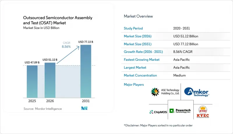
據 Mordor Intelligence 稱,2025 年外包半導體組裝和測試 (OSAT) 市場價值為 470.9 億美元,預計到 2031 年將從 2026 年的 511.2 億美元成長至 771.2 億美元,預測期(2026-2031 年)的複合年成長率為 8.56%。
本報告按服務類型(封裝和測試)、封裝類型(球柵陣列、晶片級封裝、其他)、應用(通訊、消費電子、汽車、計算和網路、其他)、技術節點(28nm 及以上、16/14nm、10/7nm、其他)和地區(北美、南美、歐洲、亞太地區、中東和非洲)進行分類。
全球外包半導體組裝測試 (OSAT) 市場趨勢與洞察
每單位半導體安裝量的激增
汽車原始設備製造商 (OEM) 正在向軟體定義平台轉型,這推高了單車半導體材料清單(BOM) 成本,並增加了對高可靠性封裝的需求。大眾汽車集團與安森美半導體在牽引逆變器方面的合作凸顯了碳化矽裝置的日益普及,而這些裝置需要具有高耐熱性的功率封裝。 IMEC 的汽車晶片專案由日月光 (ASE)、寶馬 (BMW) 和Bosch (Bosch) 支持,展示了跨價值鏈在標準化晶片封裝方面的合作,以滿足功能安全標準。因此,通過 AEC-Q100 和 ISO 26262 認證的 OSAT 供應商已獲得新的設計訂單,並成功與電動車供應商建立了多年的生產能力。
5G驅動對先進射頻封裝的需求
隨著商用 5G 基地台的部署,無線前端正向毫米波頻段轉移,這需要低損耗基板、共形屏蔽和緊湊的 SiP 封裝。 Finwave Semiconductor 在 GlobalFoundries 完成的 E 型 MISHEMT 整合標誌著一種新型氮化鎵裝置的商業化部署,該元件需要特殊的射頻封裝,目標是在 2026 年獲得量產認證。共封裝光元件已被納入 6G 測試平台流程,這要求 OSAT 公司擴展其混合訊號組裝能力和先進的散熱解決方案。
主要晶圓代工廠和整合裝置製造商的垂直整合
台積電的「晶圓製造2.0」策略,透過整合封裝和測試流程並提供承包服務,降低了獨立OSAT廠商需要處理的產量。三星也採取了類似的策略,英特爾則擴展了其代工服務,將先進的中介層技術納入其中。這些措施壓縮了第三方廠商在高利潤領域的市場佔有率,迫使OSAT廠商專注於汽車安全系統和光電等細分市場。
細分市場分析
預計2026年至2031年,測試領域的複合年成長率將達到10.35%,成長超過封裝領域的成長,但其初始規模較小。面向人工智慧和高效能運算(HPC)的設計需要系統級測試覆蓋率,以檢驗深度學習工作負載在各種電壓條件下的效能,包括晶片間的互連延遲和動態熱節流。為此,OSAT市場透過將自適應機器學習演算法整合到自動化測試設備中,提高了故障定位的準確性,同時縮短了測試時間。
2025年,封裝業務佔總銷售額的76.80%,但其組成已轉向扇出型面板、2.5D中介層和共封裝光學產品線。隨著客戶整合供應商,OSAT(外包半導體組裝測試服務商)提供整合夾具設計、最終測試和物流的承包解決方案。 Advantest透過在其V93000系列產品中增加人工智慧驅動的分析功能,連續第六年保持了其在組裝測試設備領域的領先地位。
球柵陣列(BGA)技術在主流消費和工業平台中廣泛應用,這些平台對機械強度要求極高,即使到2025年,BGA仍保持著23.85%的市場佔有率。然而,隨著行動處理器和人工智慧加速器轉向高密度線路重布,扇出型晶圓級封裝以11.02%的複合年成長率迅速擴張。這一趨勢強化了OSAT市場,因為能夠處理大尺寸面板配置且良率穩定的供應商數量有限。
日月光(ASE)投資2億美元拓展310mm x 310mm玻璃面板生產線,體現了其致力於具成本效益大面積生產的資本投入。在高頻寬記憶體堆疊中,穿透矽通孔(TSV)和玻璃通孔(TGV)的各種變體已被廣泛應用。 FC-BGA基板受益於先進製程節點的採用,並在網路ASIC中彌合了有機層壓板和矽中介層之間的差距。
區域分析
預計到2025年,亞太地區將維持其在OSAT市場收入中72.90%的佔有率,並在2031年之前維持9.45%的年複合成長率(CAGR)。台灣、中國大陸和韓國由於接近性晶圓代工廠和基板製造商,一直是該叢集的核心,但日益加劇的貿易緊張局勢促使產業集群向馬來西亞、越南和菲律賓等地多元化經營。印度加快了獎勵的實施,推動了凱因斯科技(Kaynes Technology)在古吉拉突邦投資4.13億美元的工廠以及塔塔電子(Tata Electronics)在阿薩姆邦投資30億美元的封裝測試綜合體的建設。
由於《晶片技術創新與應用法案》(CHIPS Act)的資助,北美地區重新獲得了戰略重要性。安靠(Amkor)已在亞利桑那州開始建造一座先進封裝工廠,旨在為美國國內的汽車和人工智慧客戶提供產品。德州儀器(TI)已撥款600億美元用於建造多個晶圓廠及相應的後端生產能力,而天水(SkyWater)以9300萬美元收購英飛凌(Infineon)位於奧斯汀的工廠,則提高了全國範圍內的冗餘度。
歐洲已從利基研發轉向大規模生產。 Silicon Box已獲得歐盟批准,將在義大利建造一座價值13億歐元(14.7億美元)的面板級工廠,目標是每年生產超過1億個系統級封裝(SiP)。泰雷茲、Radiall和富士康正在探索在法國建立外包半導體組裝與測試(OSAT)聯盟,以服務國防和航太領域的客戶。安森美半導體已在捷克共和國投資20億美元建造一條碳化矽(SiC)生產線,以確保電動車計畫的本地供應。中東和非洲仍然是新興市場,以色列和阿拉伯聯合大公國正在探索相關政策框架,以吸引後端投資者。
其他好處
- Excel格式的市場預測(ME)表
- 3個月的分析師支持
目錄
第1章:引言
- 研究假設和市場定義
- 調查範圍
第2章:調查方法
第3章執行摘要
第4章 市場狀況
- 市場概覽
- 市場促進因素
- 每單位半導體安裝量的激增
- 5G驅動對先進射頻封裝的需求
- 需要異質整合的AI/HPC晶片架構
- 代工廠產能不足,正在推動輕型晶圓廠外包模式的轉變。
- 透過美國《晶片晶片和晶片安全法案》(CHIPS Act)和歐盟《晶片晶片和晶片安全法案》(CHIPS Act)促進本地OSAT(外包半導體組裝和測試)的擴張
- 永續性要求正在推動晶圓級扇出技術的應用。
- 市場限制因素
- 主要晶圓代工廠和整合裝置製造商的垂直整合
- 資本投資密集度高,設備前置作業時間長
- 對先進技術的地緣政治出口限制
- 先進封裝工程領域技術純熟勞工短缺
- 價值鏈分析
- 監理情勢
- 技術展望
- 宏觀經濟因素的影響
- 波特五力分析
第5章 市場規模與成長預測
- 按服務類型
- 包裝
- 測試
- 按包裝類型
- 球柵陣列(BGA)
- 晶片級封裝(CSP)
- 四方扁平雙列直插封裝(QFP/DIP)
- 多晶片模組(MCM)
- 晶圓級封裝(WLP)
- 扇出型封裝(FO-WLP/FO-BGA)
- 系統級封裝(SiP)
- 穿透矽通孔(2.5D/3D TSV)
- 覆晶(FC-BGA/FC-CSP)
- 透過使用
- 溝通
- 家用電子產品
- 車
- 運算網路
- 產業
- 其他
- 依技術節點
- 28奈米或以上
- 16/14nm
- 10/7nm
- 5奈米或更小
- 傳統製程(90-65nm)
- 按地區
- 北美洲
- 美國
- 加拿大
- 墨西哥
- 南美洲
- 巴西
- 阿根廷
- 其他南美國家
- 歐洲
- 德國
- 法國
- 英國
- 義大利
- 荷蘭
- 俄羅斯
- 其他歐洲國家
- 亞太地區
- 中國
- 台灣
- 韓國
- 日本
- 新加坡
- 馬來西亞
- 印度
- 其他亞太國家
- 中東和非洲
- 中東
- 以色列
- 阿拉伯聯合大公國
- 沙烏地阿拉伯
- 土耳其
- 其他中東國家
- 非洲
- 南非
- 奈及利亞
- 其他非洲地區
- 中東
- 北美洲
第6章 競爭情勢
- 市場集中度
- 策略趨勢
- 市佔率分析
- 公司簡介
- ASE Technology Holding Co., Ltd.
- Amkor Technology, Inc.
- Jiangsu Changjiang Electronics Technology Co., Ltd.
- Siliconware Precision Industries Co., Ltd.
- Powertech Technology Inc.
- King Yuan Electronics Co., Ltd.
- Tongfu Microelectronics Co., Ltd.
- Tianshui Huatian Technology Co., Ltd.
- UTAC Holdings Ltd.
- Unisem(M)Berhad
- Hana Micron Inc.
- ChipMOS Technologies Inc.
- Formosa Advanced Technologies Co., Ltd.
- Chipbond Technology Corporation
- Lingsen Precision Industries, Ltd.
- Suchi Semicon Pvt. Ltd.
- Nepes Corporation
- Silicon Box Pte. Ltd.
- Shinko Electric Industries Co., Ltd.
- Carsem(M)Sdn. Bhd.
- SFA Semicon Co., Ltd.
- Stats ChipPAC Pte. Ltd.
- Orient Semiconductor Electronics, Ltd.
- Integra Technologies LLC
- Anam Semiconductor Inc.
第7章 市場機會與未來展望
According to Mordor Intelligence, the outsourced semiconductor assembly and test market size was valued at USD 47.09 billion in 2025 and estimated to grow from USD 51.12 billion in 2026 to reach USD 77.12 billion by 2031, at a CAGR of 8.56% during the forecast period (2026-2031).
This report is Segmented by Service Type (Packaging, and Testing), Packaging Type (Ball Grid Array, Chip-Scale Package, and More), Application (Communication, Consumer Electronics, Automotive, Computing and Networking, and More), Technology Node (>=28 Nm, 16/14 Nm, 10/7 Nm, and More), and Geography (North America, South America, Europe, Asia-Pacific, and Middle East and Africa).
Global Outsourced Semiconductor Assembly And Test (OSAT) Market Trends and Insights
Soaring Semiconductor Content Per Vehicle
Automotive OEMs transitioned toward software-defined platforms, lifting semiconductor bill-of-materials per car and intensifying demand for high-reliability packages. Volkswagen Group's traction inverter partnership with onsemi highlighted the rising adoption of silicon carbide devices that need thermally robust power packages.Imec's Automotive Chiplet Program, supported by ASE, BMW, and Bosch, illustrated cross-value-chain alignment on standardized chiplet packaging for functional safety compliance. OSAT providers that qualify to AEC-Q100 and ISO 26262, therefore, captured new design wins and secured multiyear capacity reservations with electric-vehicle suppliers.
5G-Led Demand for Advanced RF Packages
Commercial 5G base-station roll-outs moved the radio front-end into millimetre-wave territory, necessitating low-loss substrates, conformal shielding, and compact SiP footprints. Finwave Semiconductor's E-mode MISHEMT integration at GlobalFoundries signalled commercial deployment of novel gallium-nitride devices that require specialised RF packaging, with mass qualification targeted for 2026. The pipeline for 6G testbeds already incorporates co-packaged optics, urging OSAT firms to expand mixed-signal assembly capabilities and advanced thermal solutions.
Vertical Integration by Leading Foundries and IDMs
TSMC's Wafer Manufacturing 2.0 strategy integrated packaging and testing flows, offering turnkey services that reduced addressable volume for stand-alone OSAT companies. Samsung pursued a similar path, while Intel grew its foundry services to include advanced interposers. These moves compressed third-party share in high-margin segments and obliged OSAT firms to double down on niches such as automotive safety or photonics.
Other drivers and restraints analyzed in the detailed report include:
- AI/HPC Chiplet Architectures Needing Heterogeneous Integration
- Foundry Capacity Shortages Driving Fab-Lite Outsourcing
- Cap-Ex Intensity and Long Equipment Lead-Times
For complete list of drivers and restraints, kindly check the Table Of Contents.
Segment Analysis
Testing captured a 10.35% CAGR forecast for 2026-2031, a pace outstripping packaging's expansion yet starting from a smaller base. AI and high-performance computing designs demanded system-level test coverage that verifies chiplet interconnect latency, dynamic thermal throttling, and deep-learning workload performance under varied voltages. The outsourced semiconductor assembly and test market responded by integrating adaptive machine-learning algorithms in automatic test equipment, cutting test time while improving fault isolation.
Packaging retained 76.80% of 2025 revenue, but its composition evolved toward fan-out panel-level, 2.5D interposer, and co-packaged optics lines. As customers consolidated suppliers, OSAT groups bundled turnkey offerings that merge fixture design, final test, and logistics. Advantest secured its sixth consecutive leadership in assembly test equipment after adding AI-enabled analytics to its V93000 series.
Ball grid array technology maintained a 23.85% share in 2025 by serving mainstream consumer and industrial platforms that value mechanical robustness. However, fan-out wafer-level packages expanded at 11.02% CAGR as mobile processors and AI accelerators transitioned to high-density redistribution layers. This trend strengthened the outsourced semiconductor assembly and test market because only a limited pool of vendors can process larger panel formats without yield drift.
ASE's USD 200 million panel-level expansion to 310 mm X 310 mm glass panels illustrated a cap-ex commitment toward cost-effective, large-area builds. Through-silicon-via and through-glass-via variants proliferated in high-bandwidth memory stacks. FC-BGA substrates benefited from advanced node adoption, bridging the gap between organic laminates and silicon interposers for networking ASICs.
Complete Report Scope:
- By Service Type
- Packaging
- Testing
- By Packaging Type
- Ball Grid Array (BGA)
- Chip-Scale Package (CSP)
- Quad Flat / Dual-Inline (QFP/DIP)
- Multi-Chip Module (MCM)
- Wafer-Level Packaging (WLP)
- Fan-Out Packaging (FO-WLP / FO-BGA)
- System-in-Package (SiP)
- Through-Silicon Via (2.5D/3D TSV)
- Flip-Chip (FC-BGA / FC-CSP)
- By Application
- Communication
- Consumer Electronics
- Automotive
- Computing and Networking
- Industrial
- Other Applications
- By Technology Node
- >=28 nm
- 16/14 nm
- 10/7 nm
- 5 nm and below
- Legacy (90-65 nm)
- By Geography
- North America
- United States
- Canada
- Mexico
- South America
- Brazil
- Argentina
- Rest of South America
- Europe
- Germany
- France
- United Kingdom
- Italy
- Netherlands
- Russia
- Rest of Europe
- Asia-Pacific
- China
- Taiwan
- South Korea
- Japan
- Singapore
- Malaysia
- India
- Rest of Asia-Pacific
- Middle East and Africa
- Middle East
- Israel
- United Arab Emirates
- Saudi Arabia
- Turkey
- Rest of Middle East
- Africa
- South Africa
- Nigeria
- Rest of Africa
- Middle East
- North America
Geography Analysis
Asia-Pacific retained 72.90% share of outsourced semiconductor assembly and test market revenue in 2025 and posted a 9.45% CAGR outlook through 2031. Taiwan, China, and South Korea anchored the cluster owing to proximity to foundries and substrate makers, yet escalating trade frictions prompted diversification into Malaysia, Vietnam, and the Philippines. India accelerated incentive programmes, endorsing Kaynes Technology's USD 413 million plant in Gujarat and Tata Electronics' USD 3 billion Assam package-test complex.
North America regained strategic weight following the CHIPS Act funding. Amkor broke ground on an advanced packaging facility in Arizona designed to supply domestic automotive and AI customers. Texas Instruments earmarked USD 60 billion for multiple wafer fabs and corresponding backend capacity, while SkyWater's USD 93 million acquisition of Infineon's Austin fab added sovereign redundancy.
Europe moved from niche R&D toward scaled production. Silicon Box obtained EU approval for a EUR 1.3 billion (USD 1.47 billion) panel-level plant in Italy, targeting >100 million SiP units per year. Thales, Radiall, and Foxconn explored a French OSAT alliance to serve defence and aeronautics users. Onsemi committed USD 2 billion to a silicon-carbide line in the Czech Republic, assuring local supply for e-mobility projects. The Middle East and Africa remained an emerging frontier, with Israel and the UAE assessing policy frameworks to attract backend investors.
- ASE Technology Holding Co., Ltd.
- Amkor Technology, Inc.
- Jiangsu Changjiang Electronics Technology Co., Ltd.
- Siliconware Precision Industries Co., Ltd.
- Powertech Technology Inc.
- King Yuan Electronics Co., Ltd.
- Tongfu Microelectronics Co., Ltd.
- Tianshui Huatian Technology Co., Ltd.
- UTAC Holdings Ltd.
- Unisem (M) Berhad
- Hana Micron Inc.
- ChipMOS Technologies Inc.
- Formosa Advanced Technologies Co., Ltd.
- Chipbond Technology Corporation
- Lingsen Precision Industries, Ltd.
- Suchi Semicon Pvt. Ltd.
- Nepes Corporation
- Silicon Box Pte. Ltd.
- Shinko Electric Industries Co., Ltd.
- Carsem (M) Sdn. Bhd.
- SFA Semicon Co., Ltd.
- Stats ChipPAC Pte. Ltd.
- Orient Semiconductor Electronics, Ltd.
- Integra Technologies LLC
- Anam Semiconductor Inc.
Additional Benefits:
- The market estimate (ME) sheet in Excel format
- 3 months of analyst support
TABLE OF CONTENTS
1 INTRODUCTION
- 1.1 Study Assumptions and Market Definition
- 1.2 Scope of the Study
2 RESEARCH METHODOLOGY
3 EXECUTIVE SUMMARY
4 MARKET LANDSCAPE
- 4.1 Market Overview
- 4.2 Market Drivers
- 4.2.1 Soaring semiconductor content per vehicle
- 4.2.2 5G-led demand for advanced RF packages
- 4.2.3 AI/HPC chiplet architectures needing heterogeneous integration
- 4.2.4 Foundry capacity shortages driving fab-lite outsourcing
- 4.2.5 U.S. CHIPS and EU Chips Acts incentivising local OSAT build-out
- 4.2.6 Sustainability mandates pushing wafer-level fan-out adoption
- 4.3 Market Restraints
- 4.3.1 Vertical integration by leading foundries and IDMs
- 4.3.2 Cap-ex intensity and long equipment lead-times
- 4.3.3 Geopolitical export controls on advanced tools
- 4.3.4 Skilled-labour shortages in advanced packaging engineering
- 4.4 Value Chain Analysis
- 4.5 Regulatory Landscape
- 4.6 Technological Outlook
- 4.7 Impact of Macroeconomic Factors
- 4.8 Porter's Five Forces Analysis
- 4.8.1 Bargaining Power of Suppliers
- 4.8.2 Bargaining Power of Buyers
- 4.8.3 Threat of New Entrants
- 4.8.4 Threat of Substitutes
- 4.8.5 Intensity of Competitive Rivalry
5 MARKET SIZE AND GROWTH FORECASTS (VALUE)
- 5.1 By Service Type
- 5.1.1 Packaging
- 5.1.2 Testing
- 5.2 By Packaging Type
- 5.2.1 Ball Grid Array (BGA)
- 5.2.2 Chip-Scale Package (CSP)
- 5.2.3 Quad Flat / Dual-Inline (QFP/DIP)
- 5.2.4 Multi-Chip Module (MCM)
- 5.2.5 Wafer-Level Packaging (WLP)
- 5.2.6 Fan-Out Packaging (FO-WLP / FO-BGA)
- 5.2.7 System-in-Package (SiP)
- 5.2.8 Through-Silicon Via (2.5D/3D TSV)
- 5.2.9 Flip-Chip (FC-BGA / FC-CSP)
- 5.3 By Application
- 5.3.1 Communication
- 5.3.2 Consumer Electronics
- 5.3.3 Automotive
- 5.3.4 Computing and Networking
- 5.3.5 Industrial
- 5.3.6 Other Applications
- 5.4 By Technology Node
- 5.4.1 >=28 nm
- 5.4.2 16/14 nm
- 5.4.3 10/7 nm
- 5.4.4 5 nm and below
- 5.4.5 Legacy (90-65 nm)
- 5.5 By Geography
- 5.5.1 North America
- 5.5.1.1 United States
- 5.5.1.2 Canada
- 5.5.1.3 Mexico
- 5.5.2 South America
- 5.5.2.1 Brazil
- 5.5.2.2 Argentina
- 5.5.2.3 Rest of South America
- 5.5.3 Europe
- 5.5.3.1 Germany
- 5.5.3.2 France
- 5.5.3.3 United Kingdom
- 5.5.3.4 Italy
- 5.5.3.5 Netherlands
- 5.5.3.6 Russia
- 5.5.3.7 Rest of Europe
- 5.5.4 Asia-Pacific
- 5.5.4.1 China
- 5.5.4.2 Taiwan
- 5.5.4.3 South Korea
- 5.5.4.4 Japan
- 5.5.4.5 Singapore
- 5.5.4.6 Malaysia
- 5.5.4.7 India
- 5.5.4.8 Rest of Asia-Pacific
- 5.5.5 Middle East and Africa
- 5.5.5.1 Middle East
- 5.5.5.1.1 Israel
- 5.5.5.1.2 United Arab Emirates
- 5.5.5.1.3 Saudi Arabia
- 5.5.5.1.4 Turkey
- 5.5.5.1.5 Rest of Middle East
- 5.5.5.2 Africa
- 5.5.5.2.1 South Africa
- 5.5.5.2.2 Nigeria
- 5.5.5.2.3 Rest of Africa
- 5.5.5.1 Middle East
- 5.5.1 North America
6 COMPETITIVE LANDSCAPE
- 6.1 Market Concentration
- 6.2 Strategic Moves
- 6.3 Market Share Analysis
- 6.4 Company Profiles (includes Global level Overview, Market level Overview, Core Segments, Financials as available, Strategic Information, Market Rank/Share, Products and Services, Recent Developments)
- 6.4.1 ASE Technology Holding Co., Ltd.
- 6.4.2 Amkor Technology, Inc.
- 6.4.3 Jiangsu Changjiang Electronics Technology Co., Ltd.
- 6.4.4 Siliconware Precision Industries Co., Ltd.
- 6.4.5 Powertech Technology Inc.
- 6.4.6 King Yuan Electronics Co., Ltd.
- 6.4.7 Tongfu Microelectronics Co., Ltd.
- 6.4.8 Tianshui Huatian Technology Co., Ltd.
- 6.4.9 UTAC Holdings Ltd.
- 6.4.10 Unisem (M) Berhad
- 6.4.11 Hana Micron Inc.
- 6.4.12 ChipMOS Technologies Inc.
- 6.4.13 Formosa Advanced Technologies Co., Ltd.
- 6.4.14 Chipbond Technology Corporation
- 6.4.15 Lingsen Precision Industries, Ltd.
- 6.4.16 Suchi Semicon Pvt. Ltd.
- 6.4.17 Nepes Corporation
- 6.4.18 Silicon Box Pte. Ltd.
- 6.4.19 Shinko Electric Industries Co., Ltd.
- 6.4.20 Carsem (M) Sdn. Bhd.
- 6.4.21 SFA Semicon Co., Ltd.
- 6.4.22 Stats ChipPAC Pte. Ltd.
- 6.4.23 Orient Semiconductor Electronics, Ltd.
- 6.4.24 Integra Technologies LLC
- 6.4.25 Anam Semiconductor Inc.
7 MARKET OPPORTUNITIES AND FUTURE OUTLOOK
- 7.1 White-space and Unmet-Need Assessment

 2026-2030年全球有機矽市場
 OSAT市場報告:趨勢、預測和競爭分析(至2035年)
 半導體組裝測試外包服務市場-全球市場預測(2026-2032年)半導體組裝測試外包服務市場:依服務類型、應用、最終用戶、國家及地區分類-產業分析、市場規模、市場佔有率及2025年至2032年預測
 半導體組裝測試外包全球市場報告(2026)
 全球外包半導體組裝與測試(OSAT)市場
 半導體組裝·試驗受託(OSAT)市場,規模,佔有率,趨勢,產業分析報告:各服務形式,包裝類別,各終端用戶,各地區-2025年~2034年市場預測
 外包半導體組裝與測試市場機會、成長動力、產業趨勢分析及 2025 - 2034 年預測全球電腦網路 OSAT 市場通訊和設備全球 OSAT 市場