


 |
市場調查報告書
商品編碼
2122639
晶圓清洗設備:市場佔有率分析、產業趨勢與統計、成長預測(2026-2031)Wafer Cleaning Equipment - Market Share Analysis, Industry Trends & Statistics, Growth Forecasts (2026 - 2031) |
||||||

※ 本網頁內容可能與最新版本有所差異。詳細情況請與我們聯繫。
據 Mordor Intelligence 稱,2025 年晶圓清洗設備市值為 64.2 億美元,預計到 2031 年將從 2026 年的 69.1 億美元成長至 99.2 億美元,預測期(2026-2031 年)複合年成長率為 7.52%。
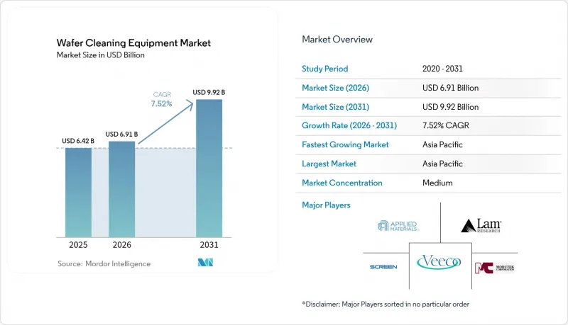
本報告依操作模式(例如,自動化設備)、技術類型(例如,單晶圓噴塗、單晶圓低溫清洗)、晶圓尺寸(150 毫米以下、200 毫米、300 毫米、450 毫米以上)、應用(例如,智慧型手機/平板電腦、南美設備)、最終用戶(代工廠、IDM、OSAT)和地區(北美、歐洲、亞太地區)進行分類、歐洲、亞太地區)。
全球晶圓清洗設備市場趨勢及洞察
3D NAND 的廣泛應用和 DRAM 的小型化推動了對無缺陷 FEOL 清洗的需求。
為實現2030年1000層3D NAND快閃記憶體的量藍圖,隨著層數的增加,晶圓清洗製程的難度也會增加一倍,因為顆粒造成的良率下降會導致清洗次數增加。 SK海力士已累計750億美元用於2028年前的記憶體小型化,其中80%將用於高頻寬記憶體。 Lam Research推出了「Cryo 3.0」蝕刻工藝,以減少深溝槽中的聚合物殘留。能夠實現亞埃級去除精度的設備製造商正受惠於層數的增加,並推動著晶圓清洗設備市場的發展。記憶體製造廠現在已將採購去除效率低於10奈米的設備作為合約條件之一,這進一步增強了長期需求。
美國、韓國和台灣鑄造產能的擴張,為設備引進創造了新的基礎。
《晶片製造和生產法案》(CHIPS Act)引發了亞利桑那州的大規模設備採購。台積電在該州的工廠需要數千台製程設備。三星和SK海力士承諾在2047年投資622兆韓元(約4,710億美元)新建16座晶圓廠,這將刺激近期訂單週期。東京電子已將其研發投入在五年內幾乎加倍,達到1.5兆日圓,以確保下一代業務的機會。產能的提升主要集中在3奈米及以下製程,這導致對先進晶圓清洗設備的需求激增,而只有參與企業市場的企業才能滿足這些設備的規格要求。設備交付週期短、服務中心位置便利,直接導致全自動清洗平台的訂單激增。
對含氟溫室氣體(F-GHGs)實施嚴格的排放法規
全球半導體產業已承諾逐步淘汰全氟辛酸(PFOA),這縮小了可用化學品的範圍。美國環保署(EPA)加快全氟烷基和多氟烷基物質(PFAS)的審查,也為化學物質藍圖增添了不確定性。 2010年至2020年間,歐洲晶圓廠已將全氟化合物(PFC)排放量減少了42%,主要透過改造加裝減排模組來實現。目前,設備製造商將洗滌器和封閉回路型化學回收系統打包銷售,這增加了實施成本,延長了投資回報期(ROI),減緩了晶圓清洗設備市場的成長預期。
細分市場分析
先進邏輯生產線對污染控制的嚴格要求,已將晶圓清洗設備市場推向「自動化優先」的模式,預計到2025年,全自動平台將佔銷售額的73.88%。半自動設備將繼續用於研發潔淨室,而手動系統仍將僅限於特殊或傳統製程。在人工智慧驅動的配方最佳化推動下,目前已佔據主導地位的全自動設備預計將以8.14%的複合年成長率持續成長。 SCREEN的SS-3200旋轉清洗機每小時可處理500片晶圓,同時還能減少去離子水的使用量,並縮短設備更換週期。
整合到設備控制器中的製程分析功能現在可以儲存每個批次數百萬個資料點,使晶圓廠能夠預測偏差並防止生產線停機。供應商正在整合預測性維護模組,這些模組可以對噴嘴污染和流量不穩定發出警告。這些數位化工作流程符合智慧製造的要求,並支援高價位。因此,晶圓清洗設備市場正在將其採購決策標準從單純的資本支出 (CAPEX) 轉向基於運轉率時間和節水效果的總擁有成本 (TCO)。
CAGR洗滌器負責去除僅靠化學方法無法處理的厚重氧化膜。
東京電子的低溫蝕刻技術減少了80%的二氧化碳排放,並印證了其綠色化學概念。 ACM Research公司的「Ultra C Tahoe」技術在保持傳統性能的同時,減少了75%的硫酸用量,已被多家晶圓代工廠採用。如今,技術決策對水和溫室氣體指標的重視程度與對顆粒計數指標的重視程度不相上下,這進一步提升了單晶圓技術創新在晶圓清洗設備市場的戰略重要性。
區域分析
預計到2025年,亞太地區將佔全球銷售額的71.92%,主要得益於台灣、韓國和中國大陸的產業叢集投資。這三個國家每月總合晶圓清洗產能將超過770萬台。高雄和新竹晶圓代工廠的擴建推動了短期設備安裝量的成長,而受出口限制影響,中國大陸IDM(整合裝置製造商)的需求激增,也促進了國內設備的普及應用。
由於台積電在亞利桑那州和英特爾在俄亥俄州的投資,北美市場佔有率有所成長,這得益於《晶片工業政策法案》(CHIPS Act)提供的津貼。這些晶圓廠被指定為美國本土服務團隊和備件中心,改變了晶圓清洗設備市場的供應商選擇趨勢。
歐洲在專業領域保持主導地位。英飛凌和義法半導體擴大了碳化矽(SiC)的生產規模,並在荷蘭投資1200萬歐元推出了“ChipNL中心”,共同開發清洗和測量平台。汽車產業的需求推動了設備的穩定更新換代。
在南美、中東和非洲,來自組裝廠的需求正在興起。阿拉伯聯合大公國和巴西的政府獎勵持續吸引需要本地晶圓清洗服務的後端工廠,預示著晶圓清洗設備市場將呈現長期的地域多元化趨勢。
其他好處:
- Excel格式的市場預測(ME)表
- 3個月的分析師支持
目錄
第1章:引言
- 研究假設和市場定義
- 調查範圍
第2章:調查方法
第3章執行摘要
第4章 市場狀況
- 市場概覽
- 市場促進因素
- 隨著 3D NAND 的日益普及和 DRAM 的小型化,對無缺陷 FEOL 清洗的需求也在不斷成長。
- 美國、韓國和台灣鑄造產能的擴張為工具的採用創造了新的基礎。
- 向 300 毫米 SiC 和 GaN 功率晶圓的過渡將需要新的濕式製程化學品。
- 由於 EUV微影術技術的普及,對小於 10 nm 的超細顆粒的清洗需求增加。
- 儘管美國實施了出口限制,但中國IDM企業仍在迅速投資晶圓廠。
- 市場限制因素
- 對含氟溫室氣體(F-GHGs)實施嚴格的排放法規
- 半導體工廠超純水(UPW)成本不斷上漲,而這些工廠又容易遭受乾旱。
- 與其他乾式等離子清洗方法相比,BEOL 的資本投資強度較高。
- 價值鏈分析
- 監管和技術展望
- 波特五力分析
- 投資分析
第5章 市場規模與成長預測
- 透過操作模式
- 自動設備
- 半自動設備
- 手動裝置
- 依技術類型
- 單片噴塗
- 單晶圓低溫
- 大量浸入
- 批次式噴霧
- 洗滌器
- 按晶圓尺寸
- 150毫米或更小
- 200 mm
- 300 mm
- 450毫米或以上
- 透過使用
- 智慧型手機和平板電腦
- 儲存裝置
- 射頻設備
- LED
- 功率分離式元件和積體電路
- CMOS影像感測器
- 最終用戶
- 鑄造廠
- 整合設備製造商(IDM)
- 半導體組裝和測試服務 (OSAT)
- 按地區
- 北美洲
- 美國
- 加拿大
- 墨西哥
- 歐洲
- 德國
- 法國
- 英國
- 北歐的
- 其他歐洲國家
- 亞太地區
- 中國
- 台灣
- 韓國
- 日本
- 印度
- 其他亞太國家
- 南美洲
- 巴西
- 墨西哥
- 阿根廷
- 其他南美國家
- 中東和非洲
- 中東
- 沙烏地阿拉伯
- 阿拉伯聯合大公國
- 土耳其
- 其他中東國家
- 非洲
- 南非
- 其他非洲國家
- 中東
- 北美洲
第6章 競爭情勢
- 市場集中度
- 策略趨勢
- 市佔率分析
- 公司簡介
- SCREEN Semiconductor Solutions Co., Ltd.
- ACM Research Inc.
- MEI Wet Processing Systems & Services LLC
- Modutek Corporation
- Akrion Technologies LLC
- RENA Technologies GmbH
- JST Manufacturing Inc.
- Yield Engineering Systems(YES)Inc.
- AP&S International GmbH
- Semsysco GmbH
- MT Systems Co., Ltd.
- Expertech Systems Inc.
- Samco Inc.
- Naura Technology Group
- Applied Materials
- Tokyo Electron Limited(TEL)
- Kaijo Corporation
- Surpass Industry Co., Ltd.
- Kingsemi Co., Ltd.
- Hwatsing Technology Co., Ltd.
第7章 市場機會與未來展望
According to Mordor Intelligence, the wafer cleaning equipment market size was valued at USD 6.42 billion in 2025 and estimated to grow from USD 6.91 billion in 2026 to reach USD 9.92 billion by 2031, at a CAGR of 7.52% during the forecast period (2026-2031).
This report is Segmented by Operating Mode (Automatic Equipment, and More), Technology Type (Single-Wafer Spray, Single-Wafer Cryogenic, and More), Wafer Size (<=150 Mm, 200 Mm, 300 Mm, and >=450 Mm), Application (Smartphones and Tablets, Memory Devices, and More), End-User (Foundries, IDM, and OSAT), and Geography (North America, Europe, Asia-Pacific, South America, and Middle East and Africa).
Global Wafer Cleaning Equipment Market Trends and Insights
Proliferation of 3-D NAND and DRAM Node Shrinks Driving Defect-Free FEOL Cleaning Demand
Mass-production roadmaps toward 1,000-layer 3-D NAND by 2030 multiply cleaning steps because every additional layer increase particle-induced yield loss. SK Hynix earmarked USD 75 billion for memory scaling through 2028, directing 80% to high-bandwidth memory. Lam Research introduced Cryo 3.0 etch to mitigate polymer residues in deep trenches. Equipment makers that deliver sub-angstrom removal precision are benefiting from rising layer counts, lifting the wafer cleaning equipment market. Memory fabs now contractually link tool purchase decisions to demonstrated removal efficiency below 10 nm, reinforcing long-term demand.
Foundry Capacity Expansion in the U.S., Korea and Taiwan Creating New Tool Install Base
The CHIPS Act triggered large-scale tool procurement in Arizona, where TSMC's complex requires thousands of process tools. Samsung and SK Hynix committed 622 trillion won (USD 471 billion) for 16 new fabs by 2047, intensifying immediate order cycles. Tokyo Electron nearly doubled R&D spend to JPY 1.5 trillion over five years to secure next-generation opportunities. Capacity additions focus on 3 nm and below, translating to tool specs that only advanced wafer cleaning equipment market participants can meet. Short tool lead-times and service proximity drove an immediate surge in orders for fully automatic cleaning platforms.
Stringent Discharge Regulations on Fluorinated Greenhouse Gases (F-GHGs)
The global semiconductor industry pledged to phase out PFOA, tightening chemical options. The U.S. EPA's accelerated PFAS review injects uncertainty into chemistry roadmaps. European fabs cut PFC emissions 42% from 2010-2020, mainly by retrofitting abatement modules. Equipment firms now bundle scrubbers and closed-loop chemical recycle units, raising acquisition cost and extending ROI timelines, moderating the wafer cleaning equipment market growth projection.
Other drivers and restraints analyzed in the detailed report include:
- Transition Toward 300 mm SiC and GaN Power Wafers Requiring New Wet-Bench Chemistries
- Adoption of EUV Lithography Necessitating Ultra-Low Particle Cleans <10 nm
- Rising Ultrapure-Water (UPW) Cost in Drought-Prone Semiconductor Hubs
For complete list of drivers and restraints, kindly check the Table Of Contents.
Segment Analysis
Fully automatic platforms generated 73.88% of 2025 revenue thanks to strict contamination-control mandates on advanced logic lines, placing the wafer cleaning equipment market in an automation-first paradigm. Semi-automatic tools persisted in R&D cleanrooms, while manual systems stayed limited to specialty or legacy flows. The fully automatic segment, already dominant, is forecast to compound at 8.14% annually on the back of AI-driven recipe optimization. SCREEN's SS-3200 spin-scrubber processed 500 wafers per hour while cutting deionized-water use, underpinning replacement cycles.
Process analytics embedded in machine controllers now store millions of datapoints per lot, allowing fabs to predict excursions and prevent line stops. Vendors embed predictive-maintenance modules that flag nozzle fouling or flow instability. These digital workflows align with smart-manufacturing mandates, supporting premium pricing. Consequently, the wafer cleaning equipment market sees purchasing decisions shift from capex alone toward total cost-of-ownership anchored in uptime metrics and water savings.
Single-wafer spray lines earned 33.05% revenue share in 2025 by combining small footprint, chemistry savings, and recipe flexibility, helping maintain the wafer cleaning equipment market trajectory. Cryogenic CO2 variants, though newer, registered the fastest 11.64% CAGR outlook on the promise of near-zero liquid discharge. Batch immersion tools survived in high-volume commodity lines, while batch spray occupied the mid-tier. Scrubbers served blanket oxide removal tasks that chemicals alone could not address.
Tokyo Electron's cryogenic etch reduced CO2 emissions 80%, validating green-chemistry claims. ACM Research's Ultra C Tahoe slashed sulfuric-acid use 75% while matching legacy performance, winning multiple foundry installs. Technology decisions now revolve around water and greenhouse-gas metrics as much as particle-count specs, reinforcing the strategic importance of single-wafer innovation to the wafer cleaning equipment market.
Complete Report Scope:
- By Operating Mode
- Automatic Equipment
- Semi-automatic Equipment
- Manual Equipment
- By Technology Type
- Single-wafer Spray
- Single-wafer Cryogenic
- Batch Immersion
- Batch Spray
- Scrubbers
- By Wafer Size
- <=150 mm
- 200 mm
- 300 mm
- >=450 mm
- By Application
- Smartphones and Tablets
- Memory Devices
- RF Devices
- LED
- Power Discrete and IC
- CMOS Image Sensors
- By End-User
- Foundries
- Integrated Device Manufacturers (IDM)
- Outsourced Semiconductor Assembly and Test (OSAT)
- By Geography
- North America
- United States
- Canada
- Mexico
- Europe
- Germany
- France
- United Kingdom
- Nordics
- Rest of Europe
- Asia-Pacific
- China
- Taiwan
- South Korea
- Japan
- India
- Rest of Asia-Pacific
- South America
- Brazil
- Mexico
- Argentina
- Rest of South America
- Middle East and Africa
- Middle East
- Saudi Arabia
- United Arab Emirates
- Turkey
- Rest of Middle East
- Africa
- South Africa
- Rest of Africa
- Middle East
- North America
Geography Analysis
Asia-Pacific generated 71.92% of 2025 revenue, anchored by cluster investments in Taiwan, South Korea, and China that collectively installed more than 7.7 million wafers per month cleaning capacity. Foundry expansions in Kaohsiung and Hsinchu lifted near-term tool uptake, while China's IDM surge under export controls catalyzed domestic tool adoption.
North America's share rose on TSMC-Arizona and Intel's Ohio investments, leveraging CHIPS Act grants. These fabs specified US-based service teams and spare-parts hubs, altering vendor-selection dynamics inside the wafer cleaning equipment market.
Europe maintained specialty leadership: Infineon and STMicroelectronics expanded SiC output; the Netherlands launched the EUR 12 million ChipNL Centre to co-develop cleaning and metrology platforms. Automotive demand underpins steady tool renewal.
South America, and Middle East and Africa posted nascent demand from assembly plants. Government incentives in the UAE and Brazil aim to attract backend facilities that still need localized wafer cleaning services, hinting at longer-term geographic diversification for the wafer cleaning equipment market.
- SCREEN Semiconductor Solutions Co., Ltd.
- ACM Research Inc.
- MEI Wet Processing Systems & Services LLC
- Modutek Corporation
- Akrion Technologies LLC
- RENA Technologies GmbH
- JST Manufacturing Inc.
- Yield Engineering Systems (YES) Inc.
- AP&S International GmbH
- Semsysco GmbH
- MT Systems Co., Ltd.
- Expertech Systems Inc.
- Samco Inc.
- Naura Technology Group
- Applied Materials
- Tokyo Electron Limited (TEL)
- Kaijo Corporation
- Surpass Industry Co., Ltd.
- Kingsemi Co., Ltd.
- Hwatsing Technology Co., Ltd.
Additional Benefits:
- The market estimate (ME) sheet in Excel format
- 3 months of analyst support
TABLE OF CONTENTS
1 INTRODUCTION
- 1.1 Study Assumptions and Market Definition
- 1.2 Scope of the Study
2 RESEARCH METHODOLOGY
3 EXECUTIVE SUMMARY
4 MARKET LANDSCAPE
- 4.1 Market Overview
- 4.2 Market Drivers
- 4.2.1 Proliferation of 3-D NAND and DRAM node shrinks driving defect-free FEOL cleaning demand
- 4.2.2 Foundry capacity expansion in the U.S., Korea and Taiwan creating new tool install base
- 4.2.3 Transition toward 300 mm SiC and GaN power wafers requiring new wet-bench chemistries
- 4.2.4 Adoption of EUV lithography necessitating ultra-low particle cleans <10 nm
- 4.2.5 Rapid fab investments by Chinese IDMs despite U.S. export controls
- 4.3 Market Restraints
- 4.3.1 Stringent discharge regulations on fluorinated greenhouse gases (F-GHGs)
- 4.3.2 Rising ultrapure water (UPW) cost in drought-prone semiconductor hubs
- 4.3.3 High capex intensity versus alternative dry plasma cleans in BEOL
- 4.4 Value Chain Analysis
- 4.5 Regulatory and Technological Outlook
- 4.6 Porter's Five Forces Analysis
- 4.6.1 Threat of New Entrants
- 4.6.2 Bargaining Power of Buyers
- 4.6.3 Bargaining Power of Suppliers
- 4.6.4 Threat of Substitutes
- 4.6.5 Intensity of Competitive Rivalry
- 4.7 Investment Analysis
5 MARKET SIZE AND GROWTH FORECASTS (VALUE)
- 5.1 By Operating Mode
- 5.1.1 Automatic Equipment
- 5.1.2 Semi-automatic Equipment
- 5.1.3 Manual Equipment
- 5.2 By Technology Type
- 5.2.1 Single-wafer Spray
- 5.2.2 Single-wafer Cryogenic
- 5.2.3 Batch Immersion
- 5.2.4 Batch Spray
- 5.2.5 Scrubbers
- 5.3 By Wafer Size
- 5.3.1 <=150 mm
- 5.3.2 200 mm
- 5.3.3 300 mm
- 5.3.4 >=450 mm
- 5.4 By Application
- 5.4.1 Smartphones and Tablets
- 5.4.2 Memory Devices
- 5.4.3 RF Devices
- 5.4.4 LED
- 5.4.5 Power Discrete and IC
- 5.4.6 CMOS Image Sensors
- 5.5 By End-User
- 5.5.1 Foundries
- 5.5.2 Integrated Device Manufacturers (IDM)
- 5.5.3 Outsourced Semiconductor Assembly and Test (OSAT)
- 5.6 By Geography
- 5.6.1 North America
- 5.6.1.1 United States
- 5.6.1.2 Canada
- 5.6.1.3 Mexico
- 5.6.2 Europe
- 5.6.2.1 Germany
- 5.6.2.2 France
- 5.6.2.3 United Kingdom
- 5.6.2.4 Nordics
- 5.6.2.5 Rest of Europe
- 5.6.3 Asia-Pacific
- 5.6.3.1 China
- 5.6.3.2 Taiwan
- 5.6.3.3 South Korea
- 5.6.3.4 Japan
- 5.6.3.5 India
- 5.6.3.6 Rest of Asia-Pacific
- 5.6.4 South America
- 5.6.4.1 Brazil
- 5.6.4.2 Mexico
- 5.6.4.3 Argentina
- 5.6.4.4 Rest of South America
- 5.6.5 Middle East and Africa
- 5.6.5.1 Middle East
- 5.6.5.1.1 Saudi Arabia
- 5.6.5.1.2 United Arab Emirates
- 5.6.5.1.3 Turkey
- 5.6.5.1.4 Rest of Middle East
- 5.6.5.2 Africa
- 5.6.5.2.1 South Africa
- 5.6.5.2.2 Rest of Africa
- 5.6.5.1 Middle East
- 5.6.1 North America
6 COMPETITIVE LANDSCAPE
- 6.1 Market Concentration
- 6.2 Strategic Moves
- 6.3 Market Share Analysis
- 6.4 Company Profiles {(includes Global level Overview, Market level overview, Core Segments, Financials as available, Strategic Information, Market Rank/Share for key companies, Products and Services, and Recent Developments)}
- 6.4.1 SCREEN Semiconductor Solutions Co., Ltd.
- 6.4.2 ACM Research Inc.
- 6.4.3 MEI Wet Processing Systems & Services LLC
- 6.4.4 Modutek Corporation
- 6.4.5 Akrion Technologies LLC
- 6.4.6 RENA Technologies GmbH
- 6.4.7 JST Manufacturing Inc.
- 6.4.8 Yield Engineering Systems (YES) Inc.
- 6.4.9 AP&S International GmbH
- 6.4.10 Semsysco GmbH
- 6.4.11 MT Systems Co., Ltd.
- 6.4.12 Expertech Systems Inc.
- 6.4.13 Samco Inc.
- 6.4.14 Naura Technology Group
- 6.4.15 Applied Materials
- 6.4.16 Tokyo Electron Limited (TEL)
- 6.4.17 Kaijo Corporation
- 6.4.18 Surpass Industry Co., Ltd.
- 6.4.19 Kingsemi Co., Ltd.
- 6.4.20 Hwatsing Technology Co., Ltd.
7 MARKET OPPORTUNITIES AND FUTURE OUTLOOK
- 7.1 White-space and Unmet-Need Assessment

 晶圓清洗設備市場-2026-2032年全球市場預測
 半導體晶圓清洗系統市場:按產品類型、技術、應用、最終用途、國家和地區分類-全球產業分析、市場規模、市場佔有率和預測(2026-2033 年)25 晶圓產能 FOUP 市場:依材料、自動化類型、密封類型、最終用戶和通路分類-2026-2032 年全球預測
 無水半導體清洗系統市場分析及預測(至2035年):依類型、產品類型、服務、技術、組件、應用、材料類型、製程、最終用戶、功能分類
 全球先進晶圓清洗技術市場:預測(至2034年)-按產品類型、清洗化學品、技術、應用、最終用戶和地區分類的分析
 2026年全球晶圓清洗設備市場報告鍊式多氣體清除和清洗設備市場:按清洗方法、技術、產能、應用、最終用戶和分銷管道分類 - 全球預測(2026-2032 年)
 晶圓清洗設備市場 - 全球產業規模、佔有率、趨勢、機會和預測,按設備類型、晶圓尺寸、功能、應用、地區和競爭格局分類,2021-2031年預測
 半導體晶圓清洗設備市場規模、佔有率及成長分析(依設備類型、晶圓尺寸、技術、操作模式及地區分類)-2026-2033年產業預測
 單晶晶片清洗設備:全球市佔率及排名、總收入及需求預測(2025-2031年)