


 |
市場調查報告書
商品編碼
2122527
薄晶圓加工和切割設備:市場佔有率分析、行業趨勢和統計數據以及成長預測(2026-2031 年)Thin Wafer Processing And Dicing Equipment - Market Share Analysis, Industry Trends & Statistics, Growth Forecasts (2026 - 2031) |
||||||

※ 本網頁內容可能與最新版本有所差異。詳細情況請與我們聯繫。
據 Mordor Intelligence 稱,2026 年薄晶圓加工和切割設備的市場規模估計為 8.2 億美元,高於 2025 年的 7.7 億美元,預計到 2031 年將達到 11.1 億美元。
預計從 2026 年到 2031 年,其複合年成長率將達到 6.32%。
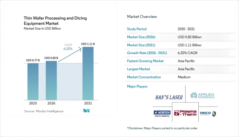
本報告按設備類型(減薄和切割設備)、應用(記憶體和邏輯TSV、MEMS裝置、功率裝置等)、晶圓厚度(750毫米、120毫米等)、晶圓尺寸(小於4英寸、5-6英寸等)以及地區(北美、南美、歐洲、亞太等)進行細分。市場預測以美元(USD)計價。
全球薄晶圓加工切割設備市場趨勢及洞察
RFID、智慧卡和汽車電源IC的應用日益廣泛。
非接觸式支付卡和汽車電氣化要求晶片厚度小於120µm,以確保高頻效率和散熱性能。用於電池式電動車(BEV)的碳化矽(SiC)牽引逆變器依賴於厚度小於100µm的晶圓以降低熱阻,從而推動了對先進研磨、化學機械拋光(CMP)和應力消除模組的需求。汽車駕駛座的數位化進一步提升了對高性能系統單晶片(SoC)的需求,而SoC則需要精確的厚度控制和低應力的晶粒分割。因此,原始設備製造商(OEM)正在製定更嚴格的厚度公差和更窄的切割寬度,這推高了高階減薄和等離子切割設備的平均售價。這一利多因素直接推動了薄晶圓加工和切割設備市場銷售的成長。
3D-IC TSV 記憶體和邏輯電路的需求激增
為了克服平面微縮的局限性,半導體製造商正轉向垂直整合。 TSV堆疊式DRAM和基於晶片組的CPU需要厚度小於50µm的晶圓,而傳統的雙面研磨系統無法在不造成晶圓翹曲的情況下完成這項製程。大型晶圓代工廠正累計數十億美元建造2nm邏輯晶片的大規模生產系統,包括大規模部署載流子解鍵合、雷射解鍵合和等離子切割設備。這種轉變進一步提高了處理容量要求。一座2nm晶圓廠每月可能需要消耗6萬片300mm晶圓,這就要求在製程的每個階段都採用超高精度定序來保護TSV側壁。因此,提供整合測量和即時應力補償功能的設備的供應商正在薄晶圓加工和切割設備市場中佔據越來越大的佔有率。
晶圓翹曲和晶片開裂導致良率下降。
當晶圓厚度減少到小於100µm時,內部應力梯度增加,導致研磨後出現明顯的翹曲。對於300mm基板,翹曲通常超過±80µm。儘管成本和複雜性增加,但對載流子和卡盤進行主動補償以校正翹曲仍然至關重要,因為在要求苛刻的TSV堆疊結構中,晶片開裂會導致10-15%的良率損失。基於等離子體的定序會產生局部熱量,而卡盤冷卻不足會加劇翹曲,因此封閉回路型溫度控管至關重要。在缺陷密度指標達到傳統的200µm基準值之前,先進減薄線的引入可能會分階段進行,預計這將減緩薄晶圓加工和切割設備市場的短期收入前景。
細分市場分析
到2025年,切割平台將佔薄晶圓加工和切割設備市場63.45%的佔有率,這反映了傳統節點和前沿節點對切割的迫切需求。由於單次切割成本指標成熟,傳統刀片系統仍主導著大規模生產的消費級積體電路市場。然而,隨著晶圓級封裝技術的進步(刀片造成的微裂紋是不可接受的),等離子切割和隱形切割系統的年訂單額正以兩位數的速度成長。預計減薄設備的複合年成長率將達到7.06%,超過通用設備的成長率,並預示架構將向厚度小於50µm的多層結構轉變。整合測量功能、無振動平台和人工智慧驅動的厚度回饋迴路正在推高平均售價(ASP),因此,就單位收入而言,減薄設備在薄晶圓加工和切割設備市場中已佔據主導地位。
市場滲透率的提升與製程節點的差異化同步進行。用於先進3D整合的晶圓通常被研磨至50µm或更薄的厚度,然後進行等離子切割。與傳統的刀片切割線相比,該製程實際上使每個晶圓的設備需求加倍。同時,成熟的邏輯和類比晶片晶圓廠正在推遲資本投資,除非處理超薄晶圓對產品性能至關重要。供應商正利用模組化底盤設計來改造現有生產線,從而縮短投資回收期,並擴大薄晶圓加工和切割設備市場的整體規模。同時,專注於無真空等離子腔室的新興參與企業正在積極吸引化合物半導體製造商,逐步從依賴刀片切割技術的老牌企業手中奪取市場佔有率,並加速競爭格局的轉變。
到2025年,用於記憶體和邏輯電路的TSV製程將佔薄晶圓加工和切割設備市場的31.80%,這主要得益於人工智慧伺服器加速器中使用的HBM模組的3D堆疊技術帶來的直接效益。同時,功率半導體將以8.16%的複合年成長率(CAGR)實現最高成長,這主要由牽引逆變器、汽車充電器以及依賴寬能隙裝置的可再生能源相關電力轉換設備所推動。這些材料需要極其乾淨的切割邊緣和高硬度,與等離子切割和隱形切割的價值提案完美契合。隨著電動車出貨量的成長,對設備的需求成長速度遠遠超過了晶圓數量的成長速度。這是因為SiC基板通常容易發生刀片斷裂,因此需要儘早過渡到使用雷射或等離子切割的個人化加工製程。
對電源領域的資本投資正在重塑薄晶圓加工和切割設備市場的成長模式。汽車OEM認證要求多站點冗餘,導致設備安裝量增加。同時,MEMS和RFID繼續以中等個位數的速度成長,為耗材主導的刀片式系統提供穩定且持續的組件銷售。 CMOS影像感測器在多相機智慧型手機和自動駕駛ADAS系統中蓬勃發展,但由於許多CIS晶圓廠轉向200mm生產線,其單價低於300mm TSV邏輯晶片。統一控制軟體使供應商能夠滿足這些多樣化的需求,從而提高客戶留存率並提升每位客戶的終身收入。
區域分析
預計到2025年,亞太地區將佔據59.65%的市場佔有率,這主要得益於台灣在晶圓代工領域的主導地位、韓國的記憶體產量以及中國政府補貼的產能擴張。該地區8.05%的複合年成長率受益於一系列晶圓廠建設項目的宣布,其中包括計劃於2026年前運作的四座2奈米製程工廠。光是這些工廠每月就需要6萬片300毫米晶圓,並需要大量的薄晶圓加工。日本設備製造商,例如迪斯科(Disco)和東京精密(Tokyo Seimitsu),供應了大部分刀片式和隱形式切割系統,而與本地供應商的接近性以及完善的售後服務進一步鞏固了亞太地區在薄晶圓加工和切割設備市場的主導地位。
北美則位居第二,這主要得益於美國刺激國內生產的產業政策。晶圓代工廠的擴張與《晶片製造法案》(CHIPS Act)的獎勵密切相關,這要求其製程性能達到與亞洲相當的水平,包括進口先進的化學機械拋光(CMP)、載流子鍵合和等離子切割技術。跨國整合裝置製造商(IDM)的大規模資本投資正在縮短設備供應商的投資回收期,並實現區域收入來源的多元化。環境、健康和安全法規促使晶圓廠採用顆粒物排放較低的等離子切割設備,而非刀片切割系統,導致北美薄晶圓加工和切割設備市場的技術模式略有變化。
歐洲的半導體戰略重點在於汽車和工業設備。在《歐洲晶片法案》的支持下,歐洲正加大對碳化矽(SiC)功率半導體晶圓廠的投資,並建造先進封裝試驗線。歐盟嚴格的排放氣體法規正在加速淘汰濕化學減薄工藝,取而代之的是閉合迴路、無磨料的化學機械拋光(CMP)和乾式雷射消熔系統。這催生了一個對環保最佳化設備而言的高階細分市場。儘管歐洲的晶圓加工量在絕對值上落後於亞太地區和北美,但高規格採購的趨勢正在推高單位平均售價,使其在全球薄晶圓加工和切割設備市場中保持領先地位。
其他好處:
- Excel格式的市場預測(ME)表
- 3個月的分析師支持
目錄
第1章:引言
- 研究假設和市場定義
- 調查範圍
第2章:調查方法
第3章執行摘要
第4章 市場狀況
- 市場概覽
- 市場促進因素
- RFID、智慧卡和汽車電源IC的應用日益廣泛。
- 3D-IC(TSV)記憶體和邏輯電路需求激增
- 家用電器正變得越來越小。
- 各鑄造廠競相投資功率超過 6 千瓦的雷射等離子切割設備。
- 中國和歐洲對3D-IC中試生產線的補貼
- 等離子切割技術在超薄SiC功率元件中的快速普及
- 市場限制因素
- 晶圓翹曲和晶片開裂導致良率下降。
- 先進的疏切/切割生產線初始成本高昂
- 適用於外延生長的超薄SiC/GaN晶片供不應求
- 加強雷射消熔產生的顆粒物的環境法規
- 產業價值鏈分析
- 監理情勢
- 技術展望
- 宏觀經濟因素對市場的影響
- 波特五力分析
第5章 市場規模與成長預測
- 依設備類型
- 疏伐設備
- 切丁裝置
- 刀切丁
- 雷射消熔
- 隱密骰子
- 等離子切割
- 透過使用
- 記憶體和邏輯(TSV)
- MEMS元件
- 功率元件
- CMOS影像感測器
- RFID
- 其他
- 按晶圓厚度
- 750µm
- 120µm
- 50µm
- 按晶圓尺寸
- 小於4英寸
- 5-6英寸
- 8吋
- 12英吋
- 按地區
- 北美洲
- 美國
- 加拿大
- 墨西哥
- 南美洲
- 巴西
- 阿根廷
- 其他南美國家
- 歐洲
- 德國
- 英國
- 法國
- 俄羅斯
- 其他歐洲國家
- 亞太地區
- 中國
- 日本
- 印度
- 韓國
- 東南亞
- 其他亞太國家
- 中東和非洲
- 中東
- 沙烏地阿拉伯
- 阿拉伯聯合大公國
- 其他中東國家
- 非洲
- 南非
- 埃及
- 其他非洲國家
- 中東
- 北美洲
第6章 競爭情勢
- 市場集中度
- 策略趨勢
- 市佔率分析
- 公司簡介
- Disco Corporation
- Tokyo Seimitsu Co., Ltd.(ACCRETECH)
- Advanced Dicing Technologies Ltd.
- Plasma-Therm LLC
- SPTS Technologies Ltd.
- Han's Laser Technology Industry Group Co., Ltd.
- ASM Laser Separation International BV
- Suzhou Delphi Laser Co., Ltd.
- Panasonic Holdings Corporation
- Hitachi High-Tech Corporation
- Applied Materials, Inc.
- Lam Research Corporation
- EV Group(EVG)
- Veeco Instruments Inc.
- Kulicke & Soffa Industries, Inc.
- TAZMO Co., Ltd.
- PVA TePla AG
- Lintec Corporation
- Synova SA
- Nidec-Read Corporation
- LASEA SA
- 3D-Micromac AG
- NAURA Technology Group Co., Ltd.
第7章 市場機會與未來展望
According to Mordor Intelligence, thin wafer processing and Dicing Equipment market size in 2026 is estimated at USD 0.82 billion, growing from 2025 value of USD 0.77 billion with 2031 projections showing USD 1.11 billion, growing at 6.32% CAGR over 2026-2031.
This report is Segmented by Equipment Type (Thinning Equipment and Dicing Equipment), Application (Memory and Logic TSV, MEMS Devices, Power Devices, and More), Wafer Thickness (750 Mm, 120 Mm, and More), Wafer Size (<4 Inch, 5-6 Inch, and More), and Geography (North America, South America, Europe, Asia-Pacific, and More). The Market Forecasts are Provided in Terms of Value (USD).
Global Thin Wafer Processing And Dicing Equipment Market Trends and Insights
Rising Adoption of RFID, Smart Cards and Automotive Power ICs
Contactless payment cards and vehicle electrification require dies with thicknesses of <=120 µm for radio-frequency efficiency and thermal performance. Silicon-carbide traction inverters in battery-electric cars rely on wafers with thicknesses below 100 µm to reduce thermal resistance, which in turn drives demand for advanced grinding, CMP, and stress-relief modules. Automotive cockpit digitalization further boosts demand for high-performance SoCs that require precise thickness control and low-stress die singulation. As a result, OEMs specify narrower thickness tolerances and lower kerf widths, lifting average selling prices for premium thinning and plasma-dicing tools. This tailwind directly supports revenue expansion in the thin wafer processing and dicing equipment market.
Surge in 3D-IC TSV Memory and Logic Demand
Chipmakers are moving toward vertical integration to bypass the limits of planar scaling. TSV-stacked DRAM and chiplet-based CPUs require wafers to be thinned to <=50 µm, which traditional double-side grind systems cannot process without inducing warpage. Leading foundries have earmarked multi-billion-dollar budgets for 2nm logic ramps that include large batches of carrier-de-bond, laser-debond, and plasma-dicing tools. The shift amplifies throughput requirements: a single 2 nm fab can consume 60,000 300 mm wafers per month, each pass obligating ultra-clean singulation to protect TSV sidewalls. Consequently, equipment suppliers offering integrated metrology and real-time stress compensation gain share inside the thin wafer processing and dicing equipment market.
Wafer Warpage and Die-Cracking Yield Losses
Reducing wafer thickness below 100 µm magnifies internal stress gradients and accentuates post-grind bow, often exceeding +-80 µm on a 300 mm substrate. Bow-corrective carriers and chuck-level active compensation add cost and complexity yet remain essential, as yield losses from die cracking can reach 10-15% in aggressive TSV stacks. Plasma-based singulation introduces localized heating, which can worsen warp if chuck cooling is inadequate, necessitating closed-loop thermal management. Until defect-density metrics match those of 200 µm historical baselines, adoption curves for advanced thinning lines may progress in staged rollouts, dampening near-term revenue potential for the thin wafer processing and dicing equipment market.
Other drivers and restraints analyzed in the detailed report include:
- Ongoing Miniaturization of Consumer Electronics
- CAPEX Race Among Foundries for >=6 kW Laser Plasma Dicing Tools
- High Upfront Cost of Advanced Thinning/Dicing Lines
For complete list of drivers and restraints, kindly check the Table Of Contents.
Segment Analysis
Dicing platforms captured 63.45% of the thin wafer processing and dicing equipment market share in 2025, reflecting the indispensable demand for die-singulation across both legacy and leading-edge nodes. Conventional blade systems still dominate high-volume consumer ICs, thanks to mature cost-per-cut metrics; however, plasma and stealth variants are registering double-digit yearly bookings as customers shift to wafer-level packages that cannot tolerate blade-induced microcracks. Thinning tools are expected to record a 7.06% CAGR, outpacing general equipment growth and signaling an architectural pivot toward sub-50 µm stacks. Integrated metrology, vibration-free stages, and AI-driven thickness feedback loops collectively raise ASPs, so the thinning segment already commands a greater revenue-per-unit ratio inside the thin wafer processing and dicing equipment market.
Market penetration parallels process-node divergence. Wafers targeted for advanced 3D integration often undergo back-grinding to a thickness of <=50 µm, followed by plasma dicing, a process that practically doubles the tool demand per wafer compared to traditional blade lines. Conversely, mature logic and analog fabs defer capex unless product performance mandates ultra-thin handling. Suppliers leverage modular chassis designs to retrofit legacy lines, shortening payback periods and expanding their total accessible Thin wafer processing and dicing equipment market size. In parallel, new entrants specializing in vacuum-less plasma chambers are courting compound semiconductor makers, nibbling away at the share of incumbents reliant on blade technology and driving competitive turnover.
Memory and logic TSV processes held 31.80% of the thin wafer processing and dicing equipment market size in 2025 due to the immediate 3D-stacking benefits within HBM modules used in AI server accelerators. Yet power semiconductors post the fastest 8.16% CAGR, fueled by traction inverters, onboard chargers, and renewables-linked power conversion that depend on wide-bandgap devices. These materials require ultra-clean kerf edges and present higher hardness, aligning perfectly with plasma and stealth dicing value propositions. As electric-vehicle unit shipments increase, tool demand intensifies far beyond proportional wafer counts, because SiC substrates typically break more blades and must transition to laser or plasma singulation early.
The power segment's capital appetite reshuffles growth share inside the thin wafer processing and dicing equipment market. Automotive OEM qualification regimes require multi-site redundancy, thereby increasing the number of equipment installations. Meanwhile, MEMS and RFID continue to experience mid-single-digit expansion, offering steady recurring parts sales for consumable-driven blade systems. CMOS image sensors are thriving in multi-camera smartphones and autonomous-driving ADAS systems; however, many CIS fabs are migrating to 200 mm lines, tempering unit value relative to 300 mm TSV logic. Suppliers that can span these divergent requirements with unified control software improve stickiness, supporting lifetime revenue per customer.
Complete Report Scope:
- By Equipment Type
- Thinning Equipment
- Dicing Equipment
- Blade Dicing
- Laser Ablation
- Stealth Dicing
- Plasma Dicing
- By Application
- Memory and Logic (TSV)
- MEMS Devices
- Power Devices
- CMOS Image Sensors
- RFID
- Others
- By Wafer Thickness
- 750 µm
- 120 µm
- 50 µm
- By Wafer Size
- <4 inch
- 5-6 inch
- 8 inch
- 12 inch
- By Geography
- North America
- United States
- Canada
- Mexico
- South America
- Brazil
- Argentina
- Rest of South America
- Europe
- Germany
- United Kingdom
- France
- Russia
- Rest of Europe
- Asia-Pacific
- China
- Japan
- India
- South Korea
- South-East Asia
- Rest of Asia-Pacific
- Middle East and Africa
- Middle East
- Saudi Arabia
- United Arab Emirates
- Rest of Middle East
- Africa
- South Africa
- Egypt
- Rest of Africa
- Middle East
- North America
Geography Analysis
Asia-Pacific's 59.65% share in 2025 stems from Taiwan's foundry leadership, South Korea's memory output, and China's subsidy-backed capacity buildout. The region's 8.05% CAGR benefits from a wave of fab announcements, including plans for four 2nm facilities coming online by 2026, which alone call for 60,000 300mm wafers per month and intensive thin-wafer processing. Japanese equipment makers, such as DISCO and Tokyo Seimitsu, supply a majority of blade and stealth dicing systems, ensuring regional vendor proximity and after-sales service density that reinforce Asia-Pacific dominance in the thin wafer processing and dicing equipment market.
North America ranks second as U.S. industrial policy stimulates domestic production. Foundry expansions linked to CHIPS Act incentives require parity with Asian process performance, including the importation of advanced CMP, carrier-bond, and plasma-dicing technologies. Large capital commitments by multinational IDMs shorten payback periods for equipment vendors and diversify geographic revenue streams. Environmental, health, and safety regulations push fabs to adopt low-particulate plasma tools over blade systems, modestly nudging technical mixes sold into the North American Thin wafer processing and dicing equipment market.
Europe's semiconductor strategy skews toward automotive and industrial devices. Investments target silicon-carbide power fabs and advanced packaging pilot lines supported by the European Chips Act. Strict emissions guidelines within the European Union are accelerating the retirement of wet-chemistry thinning paths in favor of closed-loop, abrasive-less CMP and dry laser ablation systems, thereby fostering a premium niche for environmentally optimized tools. Although Europe's absolute wafer volume trails that of the Asia-Pacific and North America, its high-specification procurement profile lifts the average revenue per tool, sustaining its contribution to the global thin wafer processing and dicing equipment market.
- Disco Corporation
- Tokyo Seimitsu Co., Ltd. (ACCRETECH)
- Advanced Dicing Technologies Ltd.
- Plasma-Therm LLC
- SPTS Technologies Ltd.
- Han's Laser Technology Industry Group Co., Ltd.
- ASM Laser Separation International B.V.
- Suzhou Delphi Laser Co., Ltd.
- Panasonic Holdings Corporation
- Hitachi High-Tech Corporation
- Applied Materials, Inc.
- Lam Research Corporation
- EV Group (EVG)
- Veeco Instruments Inc.
- Kulicke & Soffa Industries, Inc.
- TAZMO Co., Ltd.
- PVA TePla AG
- Lintec Corporation
- Synova SA
- Nidec-Read Corporation
- LASEA SA
- 3D-Micromac AG
- NAURA Technology Group Co., Ltd.
Additional Benefits:
- The market estimate (ME) sheet in Excel format
- 3 months of analyst support
TABLE OF CONTENTS
1 INTRODUCTION
- 1.1 Study Assumptions and Market Definition
- 1.2 Scope of the Study
2 RESEARCH METHODOLOGY
3 EXECUTIVE SUMMARY
4 MARKET LANDSCAPE
- 4.1 Market Overview
- 4.2 Market Drivers
- 4.2.1 Rising adoption of RFID, smart cards and automotive power ICs
- 4.2.2 Surge in 3D-IC (TSV) memory and logic demand
- 4.2.3 Ongoing miniaturisation of consumer electronics
- 4.2.4 CAPEX race among foundries for >=6 kW laser plasma dicing tools
- 4.2.5 Subsidies for 3D-IC pilot lines in China and Europe
- 4.2.6 Rapid uptake of plasma dicing for ultra-thin SiC power devices
- 4.3 Market Restraints
- 4.3.1 Wafer warpage and die-cracking yield losses
- 4.3.2 High upfront cost of advanced thinning/dicing lines
- 4.3.3 Shortage of epi-ready ultra-thin SiC/GaN wafers
- 4.3.4 Tightening environmental rules on laser ablation particulates
- 4.4 Industry Value Chain Analysis
- 4.5 Regulatory Landscape
- 4.6 Technological Outlook
- 4.7 Impact of Macroeconomic Factors on the Market
- 4.8 Porter's Five Forces Analysis
- 4.8.1 Threat of New Entrants
- 4.8.2 Bargaining Power of Buyers
- 4.8.3 Bargaining Power of Suppliers
- 4.8.4 Threat of Substitutes
- 4.8.5 Intensity of Competitive Rivalry
5 MARKET SIZE AND GROWTH FORECASTS (VALUE)
- 5.1 By Equipment Type
- 5.1.1 Thinning Equipment
- 5.1.2 Dicing Equipment
- 5.1.2.1 Blade Dicing
- 5.1.2.2 Laser Ablation
- 5.1.2.3 Stealth Dicing
- 5.1.2.4 Plasma Dicing
- 5.2 By Application
- 5.2.1 Memory and Logic (TSV)
- 5.2.2 MEMS Devices
- 5.2.3 Power Devices
- 5.2.4 CMOS Image Sensors
- 5.2.5 RFID
- 5.2.6 Others
- 5.3 By Wafer Thickness
- 5.3.1 750 µm
- 5.3.2 120 µm
- 5.3.3 50 µm
- 5.4 By Wafer Size
- 5.4.1 <4 inch
- 5.4.2 5-6 inch
- 5.4.3 8 inch
- 5.4.4 12 inch
- 5.5 By Geography
- 5.5.1 North America
- 5.5.1.1 United States
- 5.5.1.2 Canada
- 5.5.1.3 Mexico
- 5.5.2 South America
- 5.5.2.1 Brazil
- 5.5.2.2 Argentina
- 5.5.2.3 Rest of South America
- 5.5.3 Europe
- 5.5.3.1 Germany
- 5.5.3.2 United Kingdom
- 5.5.3.3 France
- 5.5.3.4 Russia
- 5.5.3.5 Rest of Europe
- 5.5.4 Asia-Pacific
- 5.5.4.1 China
- 5.5.4.2 Japan
- 5.5.4.3 India
- 5.5.4.4 South Korea
- 5.5.4.5 South-East Asia
- 5.5.4.6 Rest of Asia-Pacific
- 5.5.5 Middle East and Africa
- 5.5.5.1 Middle East
- 5.5.5.1.1 Saudi Arabia
- 5.5.5.1.2 United Arab Emirates
- 5.5.5.1.3 Rest of Middle East
- 5.5.5.2 Africa
- 5.5.5.2.1 South Africa
- 5.5.5.2.2 Egypt
- 5.5.5.2.3 Rest of Africa
- 5.5.5.1 Middle East
- 5.5.1 North America
6 COMPETITIVE LANDSCAPE
- 6.1 Market Concentration
- 6.2 Strategic Moves
- 6.3 Market Share Analysis
- 6.4 Company Profiles (includes Global-level Overview, Market-level Overview, Core Segments, Financials as available, Strategic Information, Market Rank/Share, Products and Services, Recent Developments)
- 6.4.1 Disco Corporation
- 6.4.2 Tokyo Seimitsu Co., Ltd. (ACCRETECH)
- 6.4.3 Advanced Dicing Technologies Ltd.
- 6.4.4 Plasma-Therm LLC
- 6.4.5 SPTS Technologies Ltd.
- 6.4.6 Han's Laser Technology Industry Group Co., Ltd.
- 6.4.7 ASM Laser Separation International B.V.
- 6.4.8 Suzhou Delphi Laser Co., Ltd.
- 6.4.9 Panasonic Holdings Corporation
- 6.4.10 Hitachi High-Tech Corporation
- 6.4.11 Applied Materials, Inc.
- 6.4.12 Lam Research Corporation
- 6.4.13 EV Group (EVG)
- 6.4.14 Veeco Instruments Inc.
- 6.4.15 Kulicke & Soffa Industries, Inc.
- 6.4.16 TAZMO Co., Ltd.
- 6.4.17 PVA TePla AG
- 6.4.18 Lintec Corporation
- 6.4.19 Synova SA
- 6.4.20 Nidec-Read Corporation
- 6.4.21 LASEA SA
- 6.4.22 3D-Micromac AG
- 6.4.23 NAURA Technology Group Co., Ltd.
7 MARKET OPPORTUNITIES AND FUTURE OUTLOOK
- 7.1 White-space and Unmet-need Assessment

 薄磚市場:按產品類型、材料、應用和地區分類
 單晶圓加工設備市場:依製程、晶圓尺寸、技術節點及應用分類-2026年至2032年全球預測晶圓加工設備市場:依設備類型、晶圓尺寸、技術節點和終端用戶產業分類-全球預測,2026-2032年
 薄晶圓加工和切割設備市場分析及預測(至2035年):按類型、產品類型、服務、技術、組件、應用、材料類型、製程、最終用戶和設備分類
 2026年全球晶圓加工設備市場報告
 晶圓加工設備市場-全球產業規模、佔有率、趨勢、機會、預測:按製程、應用、最終用戶、地區和競爭對手分類,2021-2031年
 薄晶圓加工切割設備市場機會、成長要素、產業趨勢分析及2026年至2035年預測
 全球晶圓切割服務市場:依材料、尺寸、切割技術與地區劃分 - 市場預測與分析 (2026-2035)
 晶圓加工與組裝設備市場-2025年至2030年預測雷射開槽設備市場(按雷射類型、操作類型、雷射功率容量、技術、應用和最終用戶分類)—2025-2030 年全球預測