

 |
市場調查報告書
商品編碼
1928874
薄晶圓加工切割設備市場機會、成長要素、產業趨勢分析及2026年至2035年預測Thin Wafer Processing and Dicing Equipment Market Opportunity, Growth Drivers, Industry Trend Analysis, and Forecast 2026 - 2035 |
||||||
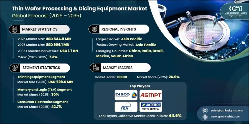
全球薄晶圓加工和切割設備市場預計到 2025 年將達到 8.448 億美元,到 2035 年將達到 17 億美元,年複合成長率為 7.3%。
半導體裝置日益複雜化以及後端製造對更高精度的需求推動了市場成長。對更薄、更輕、更可靠的組件的需求不斷成長,並持續改變整個價值鏈的設備要求。裝置結構和材料的進步使得精度、產量比率和材料應力的降低成為關注的焦點。設備供應商正積極回應,提供先進的解決方案,以實現晶圓的精確減薄和分離,同時保持結構完整性。新一代封裝技術的應用進一步提升了對高精度製程的需求。製造商優先考慮生產效率、成本效益和製程穩定性,以支援大規模半導體生產。自動化和智慧系統在提高產能、減少停機時間和加強品管發揮越來越重要的作用。這些因素共同作用,使得薄晶圓加工和切割設備成為全球半導體產業創新和規模化發展的關鍵驅動力。
| 市場覆蓋範圍 | |
|---|---|
| 開始年份 | 2025 |
| 預測年份 | 2026-2035 |
| 起始值 | 8.448億美元 |
| 預測金額 | 17億美元 |
| 複合年成長率 | 7.3% |
設備供應商不斷改進非接觸式、低應力加工技術,以提高產量比率並支援日益脆弱的晶圓結構。對尺寸精度、表面品質和運作效率的日益重視,反映了整個產業朝向更高元件密度邁進的趨勢。自動化和數據驅動系統有助於改善整個生產線的製程控制、減少缺陷並進行預測性維護。
預計到2035年,薄膜設備市場規模將達到5.996億美元。隨著半導體製造商向支援緊湊型高性能元件的超薄晶圓轉型,市場需求不斷成長。精密加工技術的持續改進有助於提高產量比率、降低應力水平,並增強與先進元件製造中使用的精密晶圓的兼容性。
預計2026年至2035年間,MEMS裝置市場將以8.6%的複合年成長率成長。成長的主要驅動力是眾多終端應用產業對緊湊、可靠、高精度元件的需求不斷成長。超薄晶圓處理和先進分離技術的日益普及提高了裝置的一致性和可靠性。自動化和即時監控系統則進一步促進了產量比率的最佳化。
歐洲薄晶圓加工和切割設備市場預計到2025年將達到1.614億美元,並在整個預測期內保持強勁成長。區域需求得益於對先進半導體製造的持續投資,尤其是在多個行業的高性能和高精度應用領域。
目錄
第1章調查方法和範圍
第2章執行摘要
第3章業界考察
- 生態系分析
- 供應商情況
- 利潤率分析
- 成本結構
- 每個階段的附加價值
- 影響價值鏈的因素
- 中斷
- 產業影響因素
- 促進要素
- 對小型化電子設備的需求不斷成長
- 5G和高效能運算應用的普及
- 擴大先進半導體材料的應用
- 汽車電子和電動車(EV)的成長
- 產業潛在風險與挑戰
- 先進切割設備高成本
- 薄晶圓的脆弱性日益增加
- 市場機遇
- 將晶圓處理與人工智慧和自動化技術結合
- MEMS、光學和射頻元件製造領域的成長
- 促進要素
- 成長潛力分析
- 監管環境
- 北美洲
- 歐洲
- 亞太地區
- 拉丁美洲
- 中東和非洲
- 波特分析
- PESTEL 分析
- 科技與創新趨勢
- 當前技術趨勢
- 新興技術
- 新興經營模式
- 合規要求
- 專利和智慧財產權分析
- 地緣政治和貿易趨勢
第4章 競爭情勢
- 介紹
- 公司市佔率分析
- 按地區
- 北美洲
- 歐洲
- 亞太地區
- 拉丁美洲
- 中東和非洲
- 按地區
- 主要企業的競爭標竿分析
- 財務績效比較
- 收入
- 利潤率
- 研究與開發
- 產品系列比較
- 產品線的廣度
- 科技
- 創新
- 區域比較
- 全球擴張分析
- 服務網路覆蓋
- 按地區分類的市場滲透率
- 競爭定位矩陣
- 領導企業
- 受讓人
- 追蹤者
- 小眾玩家
- 戰略展望矩陣
- 財務績效比較
- 2021-2024 年主要發展動態
- 併購
- 合作夥伴關係和合資企業
- 技術進步
- 擴張與投資策略
- 數位轉型計劃
- 新興/Start-Ups競賽的趨勢
第5章 依設備類型分類的市場估算與預測,2022-2035年
- 薄膜設備
- 切丁設備
- 刀切
- 雷射切割
- 隱密骰子
- 等離子切割
- 搬運輔助設備
- 臨時黏合/脫黏系統
- 晶圓安裝/拆卸系統
- 清潔和檢查系統
第6章 依晶圓尺寸分類的市場估算與預測,2022-2035年
- 小於4英寸
- 5英寸和6英寸
- 8吋
- 12英吋
第7章 依晶圓厚度分類的市場估計與預測,2022-2035年
- 750µm(標準/相對較厚)
- 120µm(先進主流)
- 50微米或更小
第8章 按應用領域分類的市場估算與預測,2022-2035年
- CMOS影像感測器
- 記憶體和邏輯(TSV)
- MEMS元件
- 功率元件
- RFID
- 其他
9. 2022-2035年按最終用途產業分類的市場估算與預測
- 家用電子電器
- 車
- 電訊
- 衛生保健
- 航太/國防
- 工業的
- 其他
第10章 2022-2035年各地區市場估計與預測
- 北美洲
- 美國
- 加拿大
- 歐洲
- 德國
- 英國
- 法國
- 西班牙
- 義大利
- 荷蘭
- 亞太地區
- 中國
- 印度
- 日本
- 澳洲
- 韓國
- 拉丁美洲
- 巴西
- 墨西哥
- 阿根廷
- 中東和非洲
- 南非
- 沙烏地阿拉伯
- 阿拉伯聯合大公國
第11章 公司簡介
- 主要企業
- DISCO Corporation
- ASMPT
- KLA Corporation
- Lam Research Corporation
- 按地區分類的主要企業
- 北美洲
- Plasma-Therm
- SPTS Technologies Ltd.
- Loadpoint Ltd.
- 歐洲
- Synova SA
- Modutek Corporation
- Dynatex International
- 亞太地區
- Tokyo Electron Limited
- TOKYO SEIMITSU CO., LTD(Accretech)
- Panasonic Connect Co., Ltd.
- 北美洲
- 小眾玩家/顛覆者
- Advanced Dicing Technologies
- AXUS TECHNOLOGY
- Citizen Chiba Precision Co., Ltd.
- HANMI Semiconductor
- Han's Laser Technology Co., Ltd.
- NeonTech Co.,Ltd.
- Suzhou Delphi Laser Co., Ltd.
The Global Thin Wafer Processing & Dicing Equipment Market was valued at USD 844.8 million in 2025 and is estimated to grow at a CAGR of 7.3% to reach USD 1.7 billion by 2035.
Market growth is supported by the rising complexity of semiconductor devices and the need for higher precision during backend manufacturing. Increasing demand for thinner, lighter, and more reliable components continues to reshape equipment requirements across the value chain. Advancements in device architecture and materials place greater emphasis on accuracy, yield improvement, and reduced material stress. Equipment suppliers respond by delivering advanced solutions that enable precise wafer thinning and separation while maintaining structural integrity. The adoption of next-generation packaging approaches further intensifies demand for high-precision processes. Manufacturers prioritize productivity, cost efficiency, and process stability to support large-scale semiconductor production. Automation and intelligent systems play an expanding role in improving throughput, reducing downtime, and enhancing quality control. Together, these factors establish thin wafer processing and dicing equipment as a critical enabler of innovation and scalability within the global semiconductor industry.
| Market Scope | |
|---|---|
| Start Year | 2025 |
| Forecast Year | 2026-2035 |
| Start Value | $844.8 Million |
| Forecast Value | $1.7 Billion |
| CAGR | 7.3% |
Equipment suppliers continue to advance non-contact and low-stress processing technologies to improve yields and support increasingly fragile wafer structures. Greater focus on dimensional accuracy, surface quality, and operational efficiency reflects broader industry trends toward higher device density. Automation and data-driven systems support improved process control, defect reduction, and predictive maintenance across manufacturing lines.
The thinning equipment segment is expected to reach USD 599.6 million by 2035. Demand rises as semiconductor producers move toward ultra-thin wafers to support compact and high-performance devices. Ongoing improvements in precision processing techniques contribute to better yield rates, lower stress levels, and enhanced compatibility with delicate wafers used in advanced device fabrication.
The MEMS devices segment is forecast to grow at a CAGR of 8.6% between 2026 and 2035. Growth is driven by expanding adoption across multiple end-use industries that require compact, reliable, and high-precision components. Increased use of ultra-thin wafer handling and advanced separation technologies improves consistency and reliability. Automation and real-time monitoring systems further support yield optimization.
Europe Thin Wafer Processing & Dicing Equipment Market accounted for USD 161.4 million in 2025 and is expected to record strong growth through the forecast period. Regional demand is supported by continued investment in advanced semiconductor manufacturing, particularly for high-performance and precision-driven applications across multiple industries.
Key companies active in the Global Thin Wafer Processing & Dicing Equipment Market include DISCO Corporation, Lam Research Corporation, ASMPT, KLA Corporation, EV Group (EVG), Han's Laser Technology Co., Ltd., Advanced Dicing Technologies, HANMI Semiconductor, AXUS TECHNOLOGY, Dynatex International, Citizen Chiba Precision Co., Ltd., and Lam Research Corporation. Companies operating in the Global Thin Wafer Processing & Dicing Equipment Market focus on strengthening their competitive position through technology innovation and product differentiation. Investment in research and development remains a core strategy to improve precision, yield, and compatibility with advanced semiconductor designs. Manufacturers expand automation and intelligent software integration to enhance productivity and reduce operational risks.
Table of Contents
Chapter 1 Methodology and Scope
- 1.1 Market scope and definition
- 1.2 Research design
- 1.2.1 Research approach
- 1.2.2 Data collection methods
- 1.3 Data mining sources
- 1.3.1 Global
- 1.3.2 Regional/Country
- 1.4 Base estimates and calculations
- 1.4.1 Base year calculation
- 1.4.2 Key trends for market estimation
- 1.5 Primary research and validation
- 1.5.1 Primary sources
- 1.6 Forecast model
- 1.7 Research assumptions and limitations
Chapter 2 Executive Summary
- 2.1 Industry 360° synopsis, 2021 - 2034
- 2.2 Key market trends
- 2.2.1 Equipment type trends
- 2.2.2 Wafer size trends
- 2.2.3 Wafer thickness trends
- 2.2.4 Application trends
- 2.2.5 End-use industry trends
- 2.2.6 Regional trends
- 2.3 TAM analysis, 2025-2034
- 2.4 CXO perspectives: Strategic imperatives
- 2.4.1 Executive decision points
- 2.4.2 Critical success factors
- 2.5 Future outlook and strategic recommendations
Chapter 3 Industry Insights
- 3.1 Industry ecosystem analysis
- 3.1.1 Supplier landscape
- 3.1.2 Profit margin analysis
- 3.1.3 Cost structure
- 3.1.4 Value addition at each stage
- 3.1.5 Factor affecting the value chain
- 3.1.6 Disruptions
- 3.2 Industry impact forces
- 3.2.1 Growth drivers
- 3.2.1.1 Rising demand for miniaturized electronic devices
- 3.2.1.2 Proliferation of 5G and high-performance computing applications
- 3.2.1.3 Increased use of advanced semiconductor materials
- 3.2.1.4 Growth in automotive electronics and EVs
- 3.2.2 Industry pitfalls and challenges
- 3.2.2.1 High costs of advanced dicing equipment
- 3.2.2.2 Increased fragility of thinned wafers
- 3.2.3 Market opportunities
- 3.2.3.1 Integration of artificial intelligence and automation in wafer handling
- 3.2.3.2 Growth in MEMS, optical, and RF device manufacturing
- 3.2.1 Growth drivers
- 3.3 Growth potential analysis
- 3.4 Regulatory landscape
- 3.4.1 North America
- 3.4.2 Europe
- 3.4.3 Asia Pacific
- 3.4.4 Latin America
- 3.4.5 Middle East & Africa
- 3.5 Porter';s analysis
- 3.6 PESTEL analysis
- 3.7 Technology and innovation landscape
- 3.7.1 Current technological trends
- 3.7.2 Emerging technologies
- 3.8 Emerging business models
- 3.9 Compliance requirements
- 3.10 Patent and IP analysis
- 3.11 Geopolitical and trade dynamics
Chapter 4 Competitive Landscape, 2024
- 4.1 Introduction
- 4.2 Company market share analysis
- 4.2.1 By region
- 4.2.1.1 North America
- 4.2.1.2 Europe
- 4.2.1.3 Asia Pacific
- 4.2.1.4 Latin America
- 4.2.1.5 Middle East & Africa
- 4.2.1 By region
- 4.3 Competitive benchmarking of key players
- 4.3.1 Financial performance comparison
- 4.3.1.1 Revenue
- 4.3.1.2 Profit margin
- 4.3.1.3 R&D
- 4.3.2 Product portfolio comparison
- 4.3.2.1 Product range breadth
- 4.3.2.2 Technology
- 4.3.2.3 Innovation
- 4.3.3 Geographic presence comparison
- 4.3.3.1 Global footprint analysis
- 4.3.3.2 Service network coverage
- 4.3.3.3 Market penetration by region
- 4.3.4 Competitive positioning matrix
- 4.3.4.1 Leaders
- 4.3.4.2 Challengers
- 4.3.4.3 Followers
- 4.3.4.4 Niche players
- 4.3.5 Strategic outlook matrix
- 4.3.1 Financial performance comparison
- 4.4 Key developments, 2021-2024
- 4.4.1 Mergers and acquisitions
- 4.4.2 Partnerships and collaborations
- 4.4.3 Technological advancements
- 4.4.4 Expansion and investment strategies
- 4.4.5 Digital transformation initiatives
- 4.5 Emerging/ startup competitors landscape
Chapter 5 Market Estimates and Forecast, By Equipment Type, 2022 - 2035 ($ Mn)
- 5.1 Key trends
- 5.2 Thinning equipment
- 5.3 Dicing equipment
- 5.3.1 Blade dicing
- 5.3.2 Laser dicing
- 5.3.3 Stealth dicing
- 5.3.4 Plasma dicing
- 5.4 Handling & support equipment
- 5.4.1 Temporary bonding/debonding systems
- 5.4.2 Wafer mounting/demounting systems
- 5.4.3 Cleaning & inspection systems
Chapter 6 Market Estimates and Forecast, By Wafer Size, 2022 - 2035 ($ Mn)
- 6.1 Key trends
- 6.2 Less than 4 inch
- 6.3 5 inch and 6 inch
- 6.4 8 inch
- 6.5 12 inch
Chapter 7 Market Estimates and Forecast, By Wafer Thickness, 2022 - 2035 ($ Mn)
- 7.1 Key trends
- 7.2 750 µm (standard / less thin)
- 7.3 120 µm (advanced mainstream)
- 7.4 50 µm and below
Chapter 8 Market Estimates and Forecast, By Application, 2022 - 2035 ($ Mn)
- 8.1 Key trends
- 8.2 CMOS image sensors
- 8.3 Memory and logic (TSV)
- 8.4 MEMS device
- 8.5 Power device
- 8.6 RFID
- 8.7 Others
Chapter 9 Market Estimates and Forecast, By End Use Industry, 2022 - 2035 ($ Mn)
- 9.1 Key trends
- 9.2 Consumer electronics
- 9.3 Automotive
- 9.4 Telecommunications
- 9.5 Healthcare
- 9.6 Aerospace & defense
- 9.7 Industrial
- 9.8 Others
Chapter 10 Market Estimates and Forecast, By Region, 2022 - 2035 ($ Mn)
- 10.1 Key trends
- 10.2 North America
- 10.2.1 U.S.
- 10.2.2 Canada
- 10.3 Europe
- 10.3.1 Germany
- 10.3.2 UK
- 10.3.3 France
- 10.3.4 Spain
- 10.3.5 Italy
- 10.3.6 Netherlands
- 10.4 Asia Pacific
- 10.4.1 China
- 10.4.2 India
- 10.4.3 Japan
- 10.4.4 Australia
- 10.4.5 South Korea
- 10.5 Latin America
- 10.5.1 Brazil
- 10.5.2 Mexico
- 10.5.3 Argentina
- 10.6 Middle East and Africa
- 10.6.1 South Africa
- 10.6.2 Saudi Arabia
- 10.6.3 UAE
Chapter 11 Company Profiles
- 11.1 Global Key Players
- 11.1.1 DISCO Corporation
- 11.1.2 ASMPT
- 11.1.3 KLA Corporation
- 11.1.4 Lam Research Corporation
- 11.2 Regional Key Players
- 11.2.1 North America
- 11.2.1.1 Plasma-Therm
- 11.2.1.2 SPTS Technologies Ltd.
- 11.2.1.3 Loadpoint Ltd.
- 11.2.2 Europe
- 11.2.2.1 Synova SA
- 11.2.2.2 Modutek Corporation
- 11.2.2.3 Dynatex International
- 11.2.3 APAC
- 11.2.3.1 Tokyo Electron Limited
- 11.2.3.2 TOKYO SEIMITSU CO., LTD (Accretech)
- 11.2.3.3 Panasonic Connect Co., Ltd.
- 11.2.1 North America
- 11.3 Niche Players / Disruptors
- 11.3.1 Advanced Dicing Technologies
- 11.3.2 AXUS TECHNOLOGY
- 11.3.3 Citizen Chiba Precision Co., Ltd.
- 11.3.4 HANMI Semiconductor
- 11.3.5 Han's Laser Technology Co., Ltd.
- 11.3.6 NeonTech Co.,Ltd.
- 11.3.7 Suzhou Delphi Laser Co., Ltd.
 單晶圓加工設備市場:依製程、晶圓尺寸、技術節點及應用分類-2026年至2032年全球預測晶圓加工設備市場:依設備類型、晶圓尺寸、技術節點和終端用戶產業分類-全球預測,2026-2032年
 薄晶圓加工和切割設備市場分析及預測(至2035年):按類型、產品類型、服務、技術、組件、應用、材料類型、製程、最終用戶和設備分類
 2026年全球晶圓加工設備市場報告
 晶圓加工設備市場-全球產業規模、佔有率、趨勢、機會、預測:按製程、應用、最終用戶、地區和競爭對手分類,2021-2031年
 全球晶圓切割服務市場:依材料、尺寸、切割技術與地區劃分 - 市場預測與分析 (2026-2035)
 薄磚市場:按產品類型、材料類型、應用和地區分類
 晶圓加工與組裝設備市場-2025年至2030年預測雷射開槽設備市場(按雷射類型、操作類型、雷射功率容量、技術、應用和最終用戶分類)—2025-2030 年全球預測
 薄晶圓加工和切割設備:市場佔有率分析、行業趨勢和成長預測(2025-2030)