


 |
市場調查報告書
商品編碼
2121346
超材料:市場佔有率分析、產業趨勢與統計、成長預測(2026-2031)Metamaterials - Market Share Analysis, Industry Trends & Statistics, Growth Forecasts (2026 - 2031) |
||||||

※ 本網頁內容可能與最新版本有所差異。詳細情況請與我們聯繫。
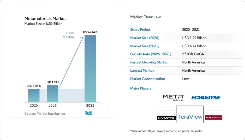
根據 Mordor Intelligence 估計,超材料市場在 2026 年的價值將達到 19.4 億美元,高於 2025 年的 15.3 億美元,預計到 2031 年將達到 64.4 億美元。
預計 2026 年至 2031 年的複合年成長率將達到 27.08%。
本報告按「類型」(電磁波、兆赫、可調諧、光子等)、「應用」(天線/雷達、感測器、隱身裝置、超透鏡等)、「終端用戶產業」(醫療、電信等)和「地區」(亞太、北美、歐洲、南美等)對產業進行分類。市場預測以美元計價。
全球超材料市場趨勢與洞察
擴展 5G 和 6G 網路規劃:用於下一代連接的超材料
基於超材料的天線正在革新毫米波傳輸,它們將波束控制硬體整合到超薄層中,同時保持Gigabit的吞吐量。在 60 GHz 頻段演示的數位編碼超表面展現了同時產生多個波束的能力,這種能力可以減少都市區的訊號屏蔽,並提升 6G 的可靠性。衛星通訊鏈路也同樣受益。2D超表面改善了非地面電波5G/6G 覆蓋的鏈路預算。商業供應商正超越實驗室原型階段,開發整合可重構智慧表面的混合衛星終端,從而確保行動平台不間斷的連接。這種輕薄硬體與軟體定義控制的融合,正為營運商在全球升級其高頻寬網路奠定持續通訊投資的基礎。
奈米技術和材料科學的進展:原子尺度的精密工程
作為國家奈米技術舉措的一部分,聯邦政府的奈米技術計畫申請了2025會計年度22億美元的預算,使累積支出超過450億美元,並建立了一個用於原子級製造的共用基礎設施。目前,逐層疊層技術能夠在整個表面上創建連續變化的屈光梯度分佈,為工程師提供了一套用於局部調節相位、振幅和偏振的工具。這種高精度正在加速超材料在結構完整性監測設備、生物醫學植入和汽車雷達外殼等領域的應用。早期使用3D列印互鎖模組製造頻率選擇性吸收器的試驗,在減少模具製造製程的同時,實現了99.5%的吸收率。這些突破性的進展降低了准入門檻,並將使主要設備製造商在中期內實現大規模生產。
對超材料優勢缺乏認知:知識差距阻礙了市場滲透。
複雜的波動物理概念令缺乏專案研發預算的產業決策者望而卻步。美國國家科學基金會(NSF) 已撥款 3.8667 億美元用於一項先進製造人才發展計劃,旨在透過實踐培訓彌合這一知識鴻溝。儘管展示小型天線和降低噪音優勢的示範計畫正在推動超材料的應用,但拉丁美洲和東南亞部分地區的中小型企業仍然面臨著較高的學習曲線。
細分市場分析
預計到2025年,電磁波相關產品將佔超材料市場銷售額的43.72%,年複合成長率達28.85%,鞏固其作為超材料市場基石的地位。電磁波相關產品在頻率選擇面板、相位陣列天線和負屈光透鏡等領域的整合應用,正推動通訊和國防領域的廣泛需求。就以金額為準,該細分市場目前佔超材料市場規模的6.6892億美元,預計到2031年將超過30.6億美元。由生物化學敏感石墨烯共振器驅動的兆赫探測技術的興起,將進一步拓展未來的商業機會。
聲學、雙曲面和負屈光等新興細分領域正在擴大超材料的功能範圍。歐盟資助的METAVISION測試支持了聲學結構在工業設備中降低機器振動的作用。雙曲面板能夠引導光子突破繞射極限,實現超高解析度成像,使其成為醫療診斷領域的實用技術。融合多種材料的混合層壓板能夠在單一層壓板內實現對聲、熱和光的多模態控制。因此,隨著研究興趣的不斷成長推動了超材料領域的多元化發展,以及大規模電磁優勢的不斷增強,超材料市場的活躍度正在不斷提升。
區域分析
北美地區佔35.45%的市場佔有率,並以28.31%的複合年成長率領先所有地區。聯邦政府對先進製造業和人才發展項目的3.8667億美元投資,正在推動一個強大的創新生態系統的發展。航太、國防和通訊領域主要企業的集中,確保了早期階段的需求,使本地供應商能夠改進其大規模生產方法。
在工業化、電子產品產能提升和大量公共資金的推動下,亞太地區也緊跟著。中國的戰略技術規劃正大力投資6G和衛星網路,加速超表面材料在基地台和行動電話天線領域的在地化應用。在生產關聯激勵計畫(PLI)的支持下,印度的電子產品生產規模正從2020-21會計年度的55.4兆盧比(約合760億美元)成長到2023-24會計年度的95.2兆盧比(約合1150億美元),為半導體級超土材料元件的發展提供了沃土材料元件的發展提供了沃土材料元件。日本和韓國正在為自動駕駛汽車和智慧工廠開發高頻雷達吸波材料。
歐洲憑藉著公私合營,在英國創新戰略和德國「工業4.0」藍圖的推動下,在先進材料領域佔據了相當大的市場佔有率。低場磁振造影和工業噪音抑制等領域的實地測試表明,歐洲已建立了一個充滿活力的合作網路。政策框架強調開放的測試平台和標準化,推動超材料市場走向跨國擴充性。
南美洲、中東和非洲是新興的前沿地區,預計將透過利用基於超材料的通訊骨幹網,大幅超越傳統基礎設施。為遠端感測器節點供電的能量能源採集型超表面符合該地區離網電氣化的優先事項,顯示一旦克服成本障礙,其潛力將充分發揮。
其他好處:
- Excel格式的市場預測(ME)表
- 3個月的分析師支持
目錄
第1章:引言
- 研究假設和市場定義
- 調查範圍
第2章:調查方法
第3章執行摘要
第4章 市場狀況
- 市場概覽
- 市場促進因素
- 5G和6G網路擴展計劃
- 奈米技術和材料科學的進展
- 加速量子運算和光電領域的發展
- 航太和國防工業的需求增加
- 人們越來越關注能源效率和永續性。
- 市場限制因素
- 對超材料優勢缺乏認知
- 超材料合成成本
- 對材料的耐久性和標準化問題感到擔憂
- 價值鏈分析
- 波特五力模型
- 專利分析
第5章 市場規模與成長預測
- 按類型
- 電磁學
- 兆赫
- 光子
- 可調
- 頻率選擇表面(FSS)
- 其他類型(聲學系統、負屈光和雙曲線系統、非線性系統、掌性系統)
- 透過使用
- 天線和雷達
- 感應器
- 隱形裝置
- 超級鏡頭
- 光線和聲音過濾
- 其他用途(太陽能熱系統、集熱器等)
- 按最終用戶行業分類
- 航太/國防
- 電訊
- 電子設備
- 衛生保健
- 其他終端使用者產業(汽車和交通運輸、能源和電力等)
- 按地區
- 亞太地區
- 中國
- 印度
- 日本
- 韓國
- 其他亞太國家
- 北美洲
- 美國
- 加拿大
- 墨西哥
- 歐洲
- 德國
- 英國
- 法國
- 義大利
- 西班牙
- 其他歐洲國家
- 南美洲
- 巴西
- 阿根廷
- 其他南美國家
- 中東和非洲
- 沙烏地阿拉伯
- 南非
- 其他中東和非洲地區
- 亞太地區
第6章 競爭情勢
- 市場集中度
- 策略趨勢
- 市佔率和排名分析
- 公司簡介
- Acoustic Metamaterials Group Limited(AMG)
- Echodyne Corp.
- Evolv Technologies, Inc.
- Fractal Antenna Systems, Inc
- JEM Engineering
- Kymeta Corporation
- Meta Materials Inc.
- Metalenz, Inc.
- Metamagnetics
- Multiwave Technologies
- Nanohmics Inc.
- Nanoscribe GmbH and Co. KG
- NanoSonic, Inc.
- NKT Photonics A/S
- Pivotal Commware
- Teraview Limited
第7章 市場機會與未來展望
According to Mordor Intelligence, metamaterials market size in 2026 is estimated at USD 1.94 billion, growing from 2025 value of USD 1.53 billion with 2031 projections showing USD 6.44 billion, growing at 27.08% CAGR over 2026-2031.
This report Segments the Industry by Type (Electromagnetic, Terahertz, Tunable, Photonic, and More), Application (Antenna and Radar, Sensors, Cloaking Devices, Superlens, and More), End-User Industry (Healthcare, Telecommunication, and More), and Geography (Asia-Pacific, North America, Europe, South America, and More). The Market Forecasts are Provided in Terms of Value (USD).
Global Metamaterials Market Trends and Insights
Expansion of 5G and 6G Network Plan: Metamaterials Enabling Next-Generation Connectivity
Metamaterial-based antennas are redefining millimeter-wave transmission by compressing beam-steering hardware into ultra-thin layers while sustaining multi-gigabit throughput. A digitally coded metasurface demonstrated at 60 GHz produced multiple simultaneous beams, a capability that mitigates urban signal blockage and underpins 6G reliability. Satellite links profit as well; 2D metasurfaces boost link budgets for non-terrestrial 5G/6G coverage. Commercial vendors have moved beyond lab prototypes, with hybrid satellite terminals integrating reconfigurable intelligent surfaces to secure uninterrupted connectivity for mobile platforms. This marriage of low-profile hardware and software-defined control positions the metamaterials market for sustained telecom spending as carriers densify high-band networks worldwide.
Advancements in Nanotechnology and Material Science: Precision Engineering at Atomic Scale
Federal programs request USD 2.2 billion for 2025 under the National Nanotechnology Initiative, lifting cumulative outlays above USD 45 billion and furnishing shared infrastructure for atomic-scale fabrication . Layer-by-layer additive methods now build graded index profiles that vary continuously across a surface, giving engineers a toolbox for tailoring phase, amplitude, and polarization locally. Such precision accelerates the insertion of metamaterials into structural health monitors, biomedical implants, and automotive radar housings. Early production trials using 3D-printed interlocking blocks to create frequency-selective absorbers reached 99.5% absorptivity while reducing tooling steps. These breakthroughs lower entry barriers and make volume output feasible for mainstream device makers over the medium term.
Lack of Awareness of Benefits of Metamaterials: Knowledge Gap Limiting Market Penetration
Complex wave-physics concepts deter decision-makers in sectors without dedicated R&D budgets. The U.S. National Science Foundation earmarked USD 386.67 million for advanced manufacturing workforce programs to bridge this gap with hands-on training . Demonstration projects that visualize gains in antenna miniaturization or noise attenuation are widening adoption, yet smaller firms in Latin America and parts of Southeast Asia still face steep learning curves.
Other drivers and restraints analyzed in the detailed report include:
- Growing Advancements in Quantum Computing and Photonics: Convergence Creating New Possibilities
- Increasing Demand from the Aerospace and Defense Industry: Strategic Applications Driving Adoption
- Cost of Synthesization of Metamaterials: Economic Barriers to Commercialization
For complete list of drivers and restraints, kindly check the Table Of Contents.
Segment Analysis
Electromagnetic variants accounted for 43.72% of 2025 revenue and are forecast to expand at 28.85% CAGR, reinforcing their role as the cornerstone of the metamaterials market. Their integration into frequency-selective panels, phased-array antennas, and negative-index lenses drives pervasive demand across telecom and defense. In value terms, this cohort represented USD 668.92 million of the metamaterials market size and is on track to cross USD 3.06 billion by 2031. The rise of terahertz detection, powered by graphene resonators with heightened biochemical sensitivity, amplifies future opportunities.
Emerging niches such as acoustic, hyperbolic, and negative-index formats broaden the functional palette. Acoustic structures dampen machinery vibration in industrial plants, supported by EU-funded METAVISION trials. Hyperbolic slabs channel sub-diffraction photons for super-resolution imaging, an asset in medical diagnostics. Hybrid stacks that fuse multiple classes unlock multi-modal control over sound, heat, and light within a single laminate. Research interest therefore accelerates diversification while reinforcing electromagnetic dominance at scale, boosting activity in the metamaterials market.
Complete Report Scope:
- By Type
- Electromagnetic
- Terahertz
- Photonic
- Tunable
- Frequency Selective Surface (FSS)
- Other Types(Acoustic, Negative-Index and Hyperbolic, Non-linear and Chiral)
- By Application
- Antenna and Radar
- Sensors
- Cloaking Devices
- Superlens
- Light and Sound Filtering
- Other Applications (Solar, Absorbers, etc.)
- By End-user Industry
- Aerospace and Defense
- Telecommunications
- Electronics
- Healthcare
- Other End user Industries (Automotive and Transportation, Energy and Power, etc.)
- By Geography
- Asia-Pacific
- China
- India
- Japan
- South Korea
- Rest of Asia-Pacific
- North America
- United States
- Canada
- Mexico
- Europe
- Germany
- United Kingdom
- France
- Italy
- Spain
- Rest of Europe
- South America
- Brazil
- Argentina
- Rest of South America
- Middle East and Africa
- Saudi Arabia
- South Africa
- Rest of Middle East Africa
- Asia-Pacific
Geography Analysis
North America translated a 35.45% stake and the highest regional CAGR of 28.31%. Federal investments of USD 386.67 million for advanced manufacturing and workforce programs reinforce a robust innovation ecosystem. Concentrated aerospace, defense, and telecom primes guarantee early-stage demand, enabling local suppliers to refine mass-production methods.
Asia-Pacific follows as industrialization and electronics capacity converge with sizable public funding. China's strategic technology plans channel resources into 6G and satellite networks, accelerating local adoption of metasurfaces for base-station and handset antennas. India's electronics output grew from INR 5.54 lakh crore (USD 76 billion) in FY 2020-21 to INR 9.52 lakh crore (USD 115 billion) in FY 2023-24 under the PLI scheme, providing fertile ground for semiconductor-grade metamaterial components. Japan and South Korea refine high-frequency radar absorbers for autonomous vehicles and smart factories.
Europe commands a sizeable share thanks to public-private programs targeting advanced materials under the UK Innovation Strategy and Germany's Industry 4.0 roadmap. Field trials in low-field MRI and industrial noise abatement testify to a thriving collaboration network. Policy frameworks emphasize open test beds and standardization, steering the metamaterials market toward cross-border scalability.
South America and the Middle East & Africa represent emerging frontiers, leveraging metamaterial-enhanced telecom backbones to leapfrog legacy infrastructure. Energy-harvesting metasurfaces that power remote sensor nodes align with regional off-grid electrification priorities, signaling untapped potential once cost barriers abate.
- Acoustic Metamaterials Group Limited (AMG)
- Echodyne Corp.
- Evolv Technologies, Inc.
- Fractal Antenna Systems, Inc
- JEM Engineering
- Kymeta Corporation
- Meta Materials Inc.
- Metalenz, Inc.
- Metamagnetics
- Multiwave Technologies
- Nanohmics Inc.
- Nanoscribe GmbH and Co. KG
- NanoSonic, Inc.
- NKT Photonics A/S
- Pivotal Commware
- Teraview Limited
Additional Benefits:
- The market estimate (ME) sheet in Excel format
- 3 months of analyst support
TABLE OF CONTENTS
1 Introduction
- 1.1 Study Assumptions and Market Definition
- 1.2 Scope of the Study
2 Research Methodology
3 Executive Summary
4 Market Landscape
- 4.1 Market Overview
- 4.2 Market Drivers
- 4.2.1 Expansion of 5G and 6G Network Plan
- 4.2.2 Advancements in Nanotechnology and Material Science
- 4.2.3 Growing Advancements in Quantum Computing and Photonics
- 4.2.4 Increasing Demand from the Aerospace and Defense Industry
- 4.2.5 Growing Emphasis on Energy Efficiency and Sustainability
- 4.3 Market Restraints
- 4.3.1 Lack of Awareness of Benefits of Metamaterials
- 4.3.2 Cost of Synthesization of Metamaterials
- 4.3.3 Concerns of Material Durability and Standardization
- 4.4 Value Chain Analysis
- 4.5 Porter's Five Forces
- 4.5.1 Bargaining Power of Suppliers
- 4.5.2 Bargaining Power of Buyers
- 4.5.3 Threat of New Entrants
- 4.5.4 Threat of Substitutes
- 4.5.5 Degree of Competition
- 4.6 Patent Analysis
5 Market Size and Growth Forecasts (Value)
- 5.1 By Type
- 5.1.1 Electromagnetic
- 5.1.2 Terahertz
- 5.1.3 Photonic
- 5.1.4 Tunable
- 5.1.5 Frequency Selective Surface (FSS)
- 5.1.6 Other Types(Acoustic, Negative-Index and Hyperbolic, Non-linear and Chiral)
- 5.2 By Application
- 5.2.1 Antenna and Radar
- 5.2.2 Sensors
- 5.2.3 Cloaking Devices
- 5.2.4 Superlens
- 5.2.5 Light and Sound Filtering
- 5.2.6 Other Applications (Solar, Absorbers, etc.)
- 5.3 By End-user Industry
- 5.3.1 Aerospace and Defense
- 5.3.2 Telecommunications
- 5.3.3 Electronics
- 5.3.4 Healthcare
- 5.3.5 Other End user Industries (Automotive and Transportation, Energy and Power, etc.)
- 5.4 By Geography
- 5.4.1 Asia-Pacific
- 5.4.1.1 China
- 5.4.1.2 India
- 5.4.1.3 Japan
- 5.4.1.4 South Korea
- 5.4.1.5 Rest of Asia-Pacific
- 5.4.2 North America
- 5.4.2.1 United States
- 5.4.2.2 Canada
- 5.4.2.3 Mexico
- 5.4.3 Europe
- 5.4.3.1 Germany
- 5.4.3.2 United Kingdom
- 5.4.3.3 France
- 5.4.3.4 Italy
- 5.4.3.5 Spain
- 5.4.3.6 Rest of Europe
- 5.4.4 South America
- 5.4.4.1 Brazil
- 5.4.4.2 Argentina
- 5.4.4.3 Rest of South America
- 5.4.5 Middle East and Africa
- 5.4.5.1 Saudi Arabia
- 5.4.5.2 South Africa
- 5.4.5.3 Rest of Middle East Africa
- 5.4.1 Asia-Pacific
6 Competitive Landscape
- 6.1 Market Concentration
- 6.2 Strategic Moves
- 6.3 Market Share (%)/Ranking Analysis
- 6.4 Company Profiles (includes Global level Overview, Market level overview, Core Segments, Financials as available, Strategic Information, Market Rank/Share, Products and Services, Recent Developments)
- 6.4.1 Acoustic Metamaterials Group Limited (AMG)
- 6.4.2 Echodyne Corp.
- 6.4.3 Evolv Technologies, Inc.
- 6.4.4 Fractal Antenna Systems, Inc
- 6.4.5 JEM Engineering
- 6.4.6 Kymeta Corporation
- 6.4.7 Meta Materials Inc.
- 6.4.8 Metalenz, Inc.
- 6.4.9 Metamagnetics
- 6.4.10 Multiwave Technologies
- 6.4.11 Nanohmics Inc.
- 6.4.12 Nanoscribe GmbH and Co. KG
- 6.4.13 NanoSonic, Inc.
- 6.4.14 NKT Photonics A/S
- 6.4.15 Pivotal Commware
- 6.4.16 Teraview Limited
7 Market Opportunities and Future Outlook
- 7.1 White-space and Unmet-need Assessment
- 7.2 Use of Metamaterials in Solar Systems
- 7.3 Metamaterial-based Radars for Drones

 超材料全球市場規模、佔有率、趨勢和成長分析報告(2026-2034)
 超材料市場-2026-2032年全球市場預測
 超材料與超表面:2034 年預測-按材料類型、結構類型、尺寸、運作頻率、功能、產品類型、應用/最終用戶和地區分類的全球分析超材料技術市場預測至2034年-按產品類型、技術、頻段、材料類型、應用、最終用戶和地區分類的全球分析
 超材料市場規模、佔有率、趨勢和預測:按類型、應用、最終用戶和地區分類,2026-2034年
 超材料市場機會、成長要素、產業趨勢分析及2026-2035年預測
 超材料市場:按產品類型、應用、終端用戶產業和地區分類
 超材料市場(至 2035 年):依超材料類型、產品形式、應用、企業規模、終端用戶產業和地區劃分:產業趨勢和全球預測聲波超材料市場:按應用、類型、材料和頻率範圍分類,全球預測(2026-2032年)
 超材料市場:依類型、產品、波控制、應用和最終用戶劃分-全球預測至2036年