


 |
市場調查報告書
商品編碼
2119387
先進半導體封裝材料:市場佔有率分析、產業趨勢與統計、成長預測(2026-2031)Semiconductor Advanced Packaging Materials - Market Share Analysis, Industry Trends & Statistics, Growth Forecasts (2026 - 2031) |
||||||

※ 本網頁內容可能與最新版本有所差異。詳細情況請與我們聯繫。
據 Mordor Intelligence 稱,2025 年半導體先進封裝材料的市場規模估計為 185.6 億美元,預計在預測期(2026-2031 年)內將以 9.06% 的複合年成長率成長,從 2026 年的 201.1 億美元成長到 2031 億美元成長到 2031 年的 3131 億美元。
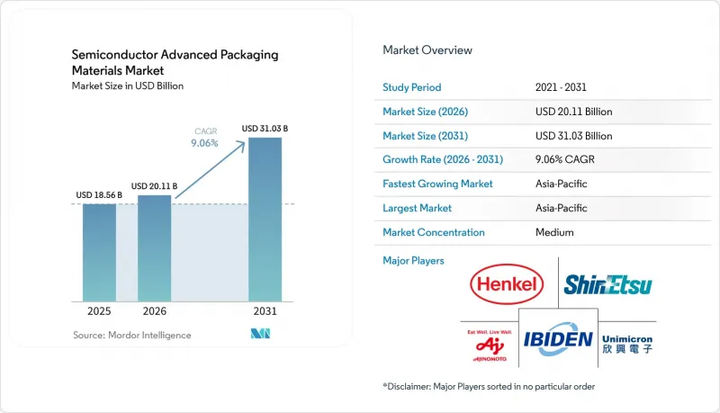
本報告按材料類型(例如基板)、封裝技術(例如覆晶封裝)、應用(例如邏輯和人工智慧處理器)以及地區(亞太地區、北美地區、歐洲地區、南美地區以及中東和非洲地區)進行細分。市場預測以美元計價。
全球半導體先進封裝材料市場趨勢及洞察
AI 和 HBM 封裝的日益複雜化正在推動材料物料清單的擴展。
隨著HBM技術的不斷演進,AI封裝所需的材料量也隨之增加。將於2026年開始量產的HBM4需要在晶片間物理界面附近使用導熱係數更高的模塑底部填充材料。 2026年5月26日,SK海力士發布了其「iHBM」散熱解決方案,該方案將矽基冷卻元件整合到HBM封裝中。據該公司稱,該方案在保持與「先進回流成型底部填充(MR-MUF)製程」相容性的同時,可將熱阻降低30%。三星的混合銅鍵合方法和SK海力士的MR-MUF製程導致了底部填充材料需要不同的認證流程。能夠快速採用客戶所選鍵合方法的供應商可以獲得認證資格,而支援多種鍵合方法的供應商則需要滿足額外的開發要求。
異質整合和晶片組的採用增加了界面層厚度。
晶片組架構在晶片之間以及晶片與中介層之間增加了介面,這需要底部填充、黏合劑和介電處理。這不僅增加了單件出貨量,也增加了每個封裝的材料需求。英特爾於2025年提交的一項專利描述了將晶片組說明層直接鍵合到主機整合電路(IC)的後端製程(BEOL)層,這可能會減少矽中介層的作用,並擴大有機線路重布(RDL)介電材料的作用。因此,封裝設計中介面和材料類型的增加將對先進半導體封裝材料市場產生影響。異質整合和混合鍵合仍然是晶片組開發的核心技術路徑。獲得代工廠認可的材料清單可能成為參與特定封裝項目的重要要求。
高昂的材料認證成本限制了新材料的採用速度。
引入新材料通常需要18至24個月的客戶認證週期。測試通常涵蓋熱循環、濕度敏感性和機械可靠性,並且往往包括晶圓級製程整合。即使在一個封裝節點上完成了認證,如果封裝形狀、層數或鍵結架構發生變化,則該認證可能不再適用於下一代產品。這項要求鞏固了現有認證供應商在先進半導體封裝材料市場中的地位。長期供應合約和已通過核准材料的產能進一步強化了這一地位。未列入2.5D和3D封裝認證供應商名單的供應商,在下一代封裝技術出現之前,可能很難進入市場。
細分市場分析
至2025年,基板將佔半導體先進封裝材料市場佔有率的41.12%。這一地位反映了基板在各種先進封裝類型中發揮的結構和電氣佈線作用。 ABF積層製造膜、覆銅層壓板和抗蝕劑構成了基板材料的核心。較大的AI伺服器封裝需要較大的單位面積基板,而積層製造薄膜的消耗量則隨著層數的增加而增加。根據IEEE電子封裝協會的數據,目前最先進的重分佈層採用2µm的線寬,目標介電常數正朝向2.0以下轉變。這些需求,以及對封裝訊號日益成長的需求,正在推動低損耗介電材料的應用。
預計2026年至2031年間,晶片黏接材料的複合年成長率將達到9.53%,成為該材料類別中成長最快的領域。燒結銀晶片黏接膜在電力電子和高密度覆晶應用中得到越來越廣泛的應用,因為傳統的聚合物漿料無法滿足這些應用的散熱和可靠性要求。隨著覆晶技術在人工智慧和高效能運算封裝中的應用日益普及,對底部填充材料的需求也不斷成長。此外,大型覆晶BGA封裝需要能夠處理低間隙高度晶片連接的材料。封裝材料支援行動裝置和物聯網設備的量產,而導熱界面材料、焊料和增厚膜也變得越來越重要。先進的半導體封裝材料產業依賴所有這些材料來平衡散熱、機械可靠性和電氣性能。
區域分析
預計到2025年,亞太地區將佔據半導體先進封裝材料市場39.18%的佔有率,並在2031年之前以9.88%的複合年成長率成長。該地區集中了先進的封裝產能和半導體材料產能。台灣仍然是積體電路基板生產的主要中心。日本向全球供應鏈供應味之素增厚膜(ABF)、封裝和先進介電聚合物。韓國在構裝基板領域保持積極的參與度,這得益於對人工智慧加速器和伺服器CPU的需求。印度正在崛起為材料應用中心和研發中心,為國內組裝和封裝計劃提供支援。
北美是人工智慧晶片設計活動最集中的地區,但其生產能力與設計需求相比仍然有限。這種缺口使得該地區依賴進口先進的封裝材料。在歐洲,奧地利的AT&S公司扮演主導角色,該公司於2025年6月在萊奧本開設了歐洲首家積體電路基板生產工廠。該計畫投資超過5億歐元,消息人士透露,實際投資額高達5.5億美元。在德國,材料供應商正積極利用漢高公司的底部填充材料、封裝和溫度控管材料產品系列來開展業務。這些優勢使歐洲在基板製造和特種材料開發領域佔據了有利地位。
即使到了2025年,南美洲、中東和非洲預計仍將對半導體先進封裝材料市場貢獻較小。墨西哥正在吸引電子製造業投資,這可能會在當地創造對封裝和黏合劑的需求,尤其是在汽車和家用電子電器組裝領域。雖然中東國家正透過國家技術計畫投資半導體供應鏈基礎設施,但該地區先進封裝材料的產能仍有限。南非和其他非洲國家則更注重下游電子組裝而非半導體封裝。這些國家未來的貢獻將取決於2020年代後半期半導體供應鏈更廣泛的區域化過程。
其他好處:
- Excel格式的市場預測(ME)表
- 3個月的分析師支持
目錄
第1章:引言
- 研究假設和市場定義
- 調查範圍
第2章:調查方法
第3章執行摘要
第4章 市場狀況
- 市場概覽
- 市場促進因素
- AI 和 HBM 封裝的日益複雜化導致材料用量增加。
- 晶片組的異質整合與應用
- 小型化、提高 I/O 密度和提高訊號傳輸速度。
- 車輛電氣化和高級駕駛輔助系統的可靠性要求
- 大型人工智慧包裝用ABF和低損耗材料的認證
- TIM1.5 與封裝級熱設計創新
- 市場限制因素
- 高昂的材料認證成本和漫長的客戶核准週期
- 先進封裝的資本密集度和收益率敏感性
- 大型封裝中翹曲係數與熱膨脹係數之間的差異
- 與 PFAS 替代品和化學品可追溯性相關的風險
- 價值鏈分析
- 波特五力分析
第5章 市場規模與成長預測
- 材料類型
- 基板
- 晶片黏接材料
- 底部填充材料
- 封裝材料
- 其他(導熱界面材料、焊接材料、黏合材料、增厚膜及其他包裝材料)
- 生產力
- 覆晶封裝
- 扇出式封裝(FOWLP/FOPLP)
- 2.5D 和 3D IC封裝
- 其他(晶圓級CSP、系統級封裝、嵌入式晶片、矽橋、混合鍵結)
- 透過使用
- 邏輯和人工智慧處理器
- 儲存裝置
- 射頻、類比和功率元件
- 其他(微機電系統和感測器、光電和光電子學)
- 按地區
- 亞太地區
- 中國
- 印度
- 日本
- 韓國
- 其他亞太國家
- 北美洲
- 美國
- 加拿大
- 墨西哥
- 歐洲
- 德國
- 英國
- 法國
- 義大利
- 其他歐洲國家
- 南美洲
- 巴西
- 阿根廷
- 其他南美國家
- 中東和非洲
- 沙烏地阿拉伯
- 南非
- 其他中東和非洲國家
- 亞太地區
第6章 競爭情勢
- 市場集中度
- 策略趨勢
- 市佔率和排名分析
- 公司簡介
- Ajinomoto Fine-Techno Co.,Inc.
- AT&S Austria Technologie & Systemtechnik Aktiengesellschaft
- Dow
- DuPont
- Henkel AG & Co. KGaA
- IBIDEN
- KYOCERA Corporation
- LG Chem
- NAMICS CORPORATION
- Nan Ya PCB Co., Ltd.
- Resonac Holdings Corporation
- SAMSUNG ELECTRO-MECHANICS
- Shin-Etsu Chemical Co., Ltd.
- SHINKO ELECTRIC INDUSTRIES
- Sumitomo Bakelite Co., Ltd.
- Unimicron
第7章 市場機會與未來展望
According to Mordor Intelligence, the semiconductor advanced packaging materials market size is estimated at USD 18.56 billion in 2025 and is estimated to grow from USD 20.11 billion in 2026 to USD 31.03 billion by 2031, at a CAGR of 9.06% during the forecast period (2026-2031).
This report is Segmented by Material Type (Substrates and More), Packaging Technology (Flip-Chip Packaging and More), Application (Logic and AI Processors and More), and Geography (Asia-Pacific, North America, Europe, South America, and Middle-East and Africa). The Market Forecasts are Provided in Terms of Value (USD).
Global Semiconductor Advanced Packaging Materials Market Trends and Insights
AI and HBM Package Complexity Driving Materials Bill-of-Materials Expansion
Each HBM generation increases the material content required in an AI package. HBM4 entered production in 2026 and requires molded underfill formulations with higher thermal conductivity near the die-to-die physical interface. SK hynix introduced its iHBM thermal solution on May 26, 2026, integrating silicon-based cooling elements into the HBM package. The company stated that the solution reduces thermal resistance by 30% while maintaining compatibility with its Advanced Mass Reflow Molded Underfill (MR-MUF) process. Samsung's hybrid copper bonding route and SK hynix's MR-MUF approach create separate qualification paths for underfill materials. Suppliers that align early with a customer's selected bonding route can secure qualified status, while suppliers serving multiple routes face additional development requirements.
Heterogeneous Integration and Chiplet Adoption Multiplying Interface Layers
Chiplet architectures add die-to-die and die-to-interposer interfaces that require underfill, adhesive, and dielectric treatment. This increases the material requirement for each package rather than simply increasing unit shipments. Intel's 2025 patent filings described chiplet metallization directly bonded to host integrated circuit (IC) back-end-of-line layers, which could reduce the role of silicon interposers and increase the role of organic redistribution-layer dielectric materials. Therefore, the semiconductor advanced packaging materials market is affected when package designs use more interfaces and more material types. Heterogeneous integration and hybrid bonding remain central technology paths for chiplet development. Foundry-approved material lists can become a practical requirement for participation in specialized packaging programs.
High Material Qualification Costs Constraining New Material Adoption Velocity
New materials often require an 18- to 24-month customer qualification cycle. Testing typically covers thermal cycling, moisture sensitivity, mechanical reliability, and, in many cases, wafer-level process integration. A completed qualification for one packaging node may not apply to the next generation if package geometry, layer count, or bonding architecture changes. This requirement strengthens the position of existing approved suppliers in the semiconductor advanced packaging materials market. Long-term supply agreements and capacity reservations for approved materials further support this position. Suppliers outside approved vendor lists for 2.5D and 3D packaging may have limited opportunities to enter the market before the next package generation.
Other drivers and restraints analyzed in the detailed report include:
- ABF and Low-Loss Material Qualification Creating Structural Supply Constraints
- TIM1.5 and Package-Level Thermal Innovation Emerging as a Distinct Market Segment
- PFAS Substitution and Chemical Traceability: Introducing Multi-Year Compliance Costs
For complete list of drivers and restraints, kindly check the Table Of Contents.
Segment Analysis
Substrates accounted for 41.12% of the semiconductor advanced packaging materials market share in 2025. Their position reflected the structural and electrical routing role they play across advanced package types. ABF build-up film, copper-clad laminates, and solder resist form the core substrate material set. Larger AI server packages require more substrate area per unit, while higher layer counts increase build-up film consumption. The IEEE Electronics Packaging Society states that leading redistribution-layer implementations now use 2 µm linewidths, while target dielectric constants are moving toward 2.0 or below. These requirements support the use of low-loss dielectric materials as demand for package signals increases.
Die attach materials are expected to register a 9.53% CAGR from 2026 to 2031, the highest growth rate within this material grouping. Sintered silver die attach films are gaining use in power electronics and dense flip-chip applications, where conventional polymer pastes cannot meet thermal and reliability requirements. Underfill demand is rising with the deeper adoption of flip-chip technology in AI and high-performance computing packages. Large-body flip-chip BGA configurations also require materials that can manage low-gap-height die connections. Encapsulation materials support high-volume mobile and IoT assembly, while thermal interface materials, solder materials, and build-up films are becoming more important. The semiconductor advanced packaging materials industry relies on all these categories to balance heat removal, mechanical reliability, and electrical performance.
Complete Report Scope:
- By Material Type
- Substrates
- Die Attach Materials
- Underfill Materials
- Encapsulation Materials
- Others (Thermal Interface Materials, Solder Materials, Bonding Materials, Build-Up Films and Other Packaging Materials)
- By Packaging Technology
- Flip-Chip Packaging
- Fan-Out Packaging (FOWLP/FOPLP)
- 2.5D and 3D IC Packaging
- Others (Wafer-Level CSP, System-in-Package, Embedded-Die, Silicon Bridge and Hybrid Bonding)
- By Application
- Logic and AI Processors
- Memory Devices
- RF, Analog and Power Devices
- Others (MEMS and Sensors, Photonics and Optoelectronics)
- By Geography
- Asia-Pacific
- China
- India
- Japan
- South Korea
- Rest of Asia-Pacific
- North America
- United States
- Canada
- Mexico
- Europe
- Germany
- United Kingdom
- France
- Italy
- Rest of Europe
- South America
- Brazil
- Argentina
- Rest of South America
- Middle-East and Africa
- Saudi Arabia
- South Africa
- Rest of Middle-East and Africa
- Asia-Pacific
Geography Analysis
Asia-Pacific held 39.18% of the semiconductor advanced packaging materials market share in 2025 and is forecast to grow at a CAGR of 9.88% through 2031. The region has a high concentration of advanced packaging capacity and semiconductor materials production. Taiwan remains a key hub for IC substrate production. Japan supplies Ajinomoto Build-up Film (ABF), encapsulants, and advanced dielectric polymers to global supply chains. South Korea maintains strong activity in package substrates, supported by demand for AI accelerators and server CPUs. India is emerging as a secondary location for materials applications and innovation centers that support national assembly and packaging plans.
North America has the largest concentration of AI chip design activity, but its production assets remain limited relative to design demand. This gap keeps the region dependent on imported advanced packaging materials. Europe is led by Austria's AT&S, which opened Europe's first IC substrate production facility in Leoben in June 2025. The project included an investment exceeding EUR 500 million, which the source reported as USD 550 million. Germany has substantial materials supplier activity through Henkel's portfolio of underfills, encapsulants, and thermal management materials. These capabilities position Europe in substrate manufacturing and specialty materials development.
South America, the Middle-East, and Africa remained minor contributors to the advanced packaging materials market for semiconductors in 2025. Mexico is attracting electronics manufacturing investment, which could create local demand for encapsulants and adhesives, particularly in automotive and consumer electronics assembly. Middle-Eastern countries are investing in semiconductor supply chain infrastructure through national technology programs, although advanced packaging materials capacity in the region remains limited. South Africa and other African locations remain focused on downstream electronics assembly rather than semiconductor packaging. Their future contribution depends on the broader regionalization of the semiconductor supply chain through the late 2020s.
- Ajinomoto Fine-Techno Co.,Inc.
- AT&S Austria Technologie & Systemtechnik Aktiengesellschaft
- Dow
- DuPont
- Henkel AG & Co. KGaA
- IBIDEN
- KYOCERA Corporation
- LG Chem
- NAMICS CORPORATION
- Nan Ya PCB Co., Ltd.
- Resonac Holdings Corporation
- SAMSUNG ELECTRO-MECHANICS
- Shin-Etsu Chemical Co., Ltd.
- SHINKO ELECTRIC INDUSTRIES
- Sumitomo Bakelite Co., Ltd.
- Unimicron
Additional Benefits:
- The market estimate (ME) sheet in Excel format
- 3 months of analyst support
TABLE OF CONTENTS
1 Introduction
- 1.1 Study Assumptions and Market Definition
- 1.2 Scope of the Study
2 Research Methodology
3 Executive Summary
4 Market Landscape
- 4.1 Market Overview
- 4.2 Market Drivers
- 4.2.1 AI and HBM Package Complexity Increasing Materials Content
- 4.2.2 Heterogeneous Integration and Chiplet Adoption
- 4.2.3 Miniaturization, Higher I/O Density, and Faster Signal Transmission
- 4.2.4 Automotive Electrification and ADAS Reliability Requirements
- 4.2.5 ABF and Low-Loss Material Qualification for Large AI Packages
- 4.2.6 TIM1.5 and Package-Level Thermal Innovation
- 4.3 Market Restraints
- 4.3.1 High Material Qualification Costs and Long Customer Approval Cycles
- 4.3.2 Capital Intensity and Yield Sensitivity in Advanced Packaging
- 4.3.3 Warpage and Coefficient-of-Thermal-Expansion Mismatch in Large Packages
- 4.3.4 PFAS Substitution and Chemical Traceability Risk
- 4.4 Value Chain Analysis
- 4.5 Porter's Five Forces Analysis
- 4.5.1 Bargaining Power of Suppliers
- 4.5.2 Bargaining Power of Buyers
- 4.5.3 Threat of New Entrants
- 4.5.4 Threat of Substitutes
- 4.5.5 Competitive Rivalry
5 Market Size and Growth Forecasts (Value)
- 5.1 By Material Type
- 5.1.1 Substrates
- 5.1.2 Die Attach Materials
- 5.1.3 Underfill Materials
- 5.1.4 Encapsulation Materials
- 5.1.5 Others (Thermal Interface Materials, Solder Materials, Bonding Materials, Build-Up Films and Other Packaging Materials)
- 5.2 By Packaging Technology
- 5.2.1 Flip-Chip Packaging
- 5.2.2 Fan-Out Packaging (FOWLP/FOPLP)
- 5.2.3 2.5D and 3D IC Packaging
- 5.2.4 Others (Wafer-Level CSP, System-in-Package, Embedded-Die, Silicon Bridge and Hybrid Bonding)
- 5.3 By Application
- 5.3.1 Logic and AI Processors
- 5.3.2 Memory Devices
- 5.3.3 RF, Analog and Power Devices
- 5.3.4 Others (MEMS and Sensors, Photonics and Optoelectronics)
- 5.4 By Geography
- 5.4.1 Asia-Pacific
- 5.4.1.1 China
- 5.4.1.2 India
- 5.4.1.3 Japan
- 5.4.1.4 South Korea
- 5.4.1.5 Rest of Asia-Pacific
- 5.4.2 North America
- 5.4.2.1 United States
- 5.4.2.2 Canada
- 5.4.2.3 Mexico
- 5.4.3 Europe
- 5.4.3.1 Germany
- 5.4.3.2 United Kingdom
- 5.4.3.3 France
- 5.4.3.4 Italy
- 5.4.3.5 Rest of Europe
- 5.4.4 South America
- 5.4.4.1 Brazil
- 5.4.4.2 Argentina
- 5.4.4.3 Rest of South America
- 5.4.5 Middle-East and Africa
- 5.4.5.1 Saudi Arabia
- 5.4.5.2 South Africa
- 5.4.5.3 Rest of Middle-East and Africa
- 5.4.1 Asia-Pacific
6 Competitive Landscape
- 6.1 Market Concentration
- 6.2 Strategic Moves
- 6.3 Market Share (%)/Ranking Analysis
- 6.4 Company Profiles (includes Global Overview, Market Overview, Core Segments, Financials as available, Strategic Information, Products and Services, and Recent Developments)
- 6.4.1 Ajinomoto Fine-Techno Co.,Inc.
- 6.4.2 AT&S Austria Technologie & Systemtechnik Aktiengesellschaft
- 6.4.3 Dow
- 6.4.4 DuPont
- 6.4.5 Henkel AG & Co. KGaA
- 6.4.6 IBIDEN
- 6.4.7 KYOCERA Corporation
- 6.4.8 LG Chem
- 6.4.9 NAMICS CORPORATION
- 6.4.10 Nan Ya PCB Co., Ltd.
- 6.4.11 Resonac Holdings Corporation
- 6.4.12 SAMSUNG ELECTRO-MECHANICS
- 6.4.13 Shin-Etsu Chemical Co., Ltd.
- 6.4.14 SHINKO ELECTRIC INDUSTRIES
- 6.4.15 Sumitomo Bakelite Co., Ltd.
- 6.4.16 Unimicron
7 Market Opportunities and Future Outlook
- 7.1 White-Space and Unmet-Need Assessment

 2026年全球半導體濕化學品市場報告2026年電子和半導體應用濕化學品全球市場報告2026年全球半導體製程化學品市場報告
 半導體濕化學品市場預測至2034年-按產品、純度等級、製程、晶圓尺寸、最終用戶和地區分類的全球分析
 用於DRAM濕式製程的高純度化學品:市場佔有率分析、行業趨勢和統計數據以及成長預測(2026-2031年)
 故障分析設備市場:依設備、技術、應用、地區分類先進微影術材料市場預測至2034年—按材料類型、微影術技術、波長類型、應用、最終用戶和地區分類的全球分析半導體製造市場:依可追溯性方法、應用和地區分類
 半導體用高介電常數前驅體市場報告:趨勢、預測與競爭分析(至2035年)熔融石英窗市場報告:趨勢、預測與競爭分析(至2035年)