


 |
市場調查報告書
商品編碼
2099469
用於DRAM濕式製程的高純度化學品:市場佔有率分析、行業趨勢和統計數據以及成長預測(2026-2031年)High-Purity Chemicals For DRAM Wet Processing - Market Share Analysis, Industry Trends & Statistics, Growth Forecasts (2026 - 2031) |
||||||

※ 本網頁內容可能與最新版本有所差異。詳細情況請與我們聯繫。
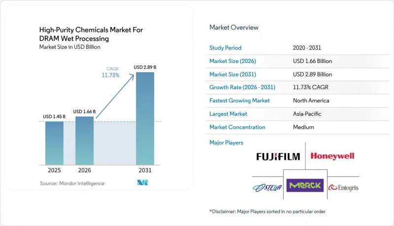
據 Mordor Intelligence 稱,DRAM 濕式製程用高純度化學品的市場規模預計將從 2025 年的 14.5 億美元成長到 2026 年的 16.6 億美元,到 2031 年達到 28.9 億美元,預計 2026 年至 2031 年的複合年成長率為 17%。
本報告按化學物質類型(酸、鹼、溶劑等)、製程應用(晶圓清洗、光阻劑剝離等)、純度等級(SEMI 5級[先進DRAM節點]、SEMI 4級[成熟DRAM節點]等)、DRAM產品類型(DDR5 DRAM、HBM DRAM、DDR4 DRAM節點]等)、DRAM產品類型(DDR5 DRAM、HBM DRAM、DDR4 DRAM等)和地區進行細分。市場預測以美元(USD)計價。
DRAM濕式製程以高純度化學品市場洞察與趨勢
隨著DRAM節點尺寸的減小,濕式清洗的頻率也隨之增加。
隨著DRAM節點小型化進程的推進,每片晶圓的濕式清洗步驟數量不斷增加,純度要求也日益嚴格,導致DRAM濕式製程用高純度化學品市場需求持續成長。研究表明,從N90到A14製程節點,濕式製程佔整個製程化學品總消耗量的35%至59%,即使在先進的小型化製程中,濕式製程仍是化學品使用的重要組成部分。這一趨勢表明,即使晶圓生產啟動緩慢,化學品需求也可能繼續成長,因為處理每片晶圓完成整個製程需要更多的化學品。此外,向1-BETA和1-γ結構的過渡增加了薄膜沉積、選擇性蝕刻和殘留物去除等工藝,從而增加了所需的清洗循環次數。已經符合SEMI C1液體化學品認證分析架構的供應商,在客戶逐代重新認證化學品的過程中,更有利於維持其現有地位。因此,DRAM濕式製程用高純度化學品的市場不僅與產量密切相關,而且與技術轉型和良率管理也密切相關。
高頻寬記憶體(HBM)的擴展推動了對先進表面處理技術的需求。
由於與傳統的平面記憶體製程相比,HBM 在 TSV 形成、層間鍵結和蝕刻後清洗等方面需要更嚴格的表面控制,因此它是對化學要求最高的 DRAM 格式之一。據應用材料公司稱,近年來 HBM 的產量以約 50% 的複合年成長率成長,這一成長速度支撐了對先進 DRAM 晶圓加工和相關材料技術的強勁需求。隨著 TSV 尺寸的縮小和長寬比的增加,殘留物去除變得更加精細,對顆粒物和微量污染物的容忍度也更低。這提高了對化學品等級的要求,並增加了每片晶圓的化學品消耗量,尤其是在 TSV 形成後和鍵合前的表面處理製程。 HBM 在 DRAM 濕式製程的高純度化學品市場中佔據重要地位,不僅因為其快速成長,還因為它將收入轉向了高附加價值配方。因此,專注於混合鍵合和先進表面處理化學品的供應商比僅專注於傳統 DDR 製程的供應商更有優勢,能夠獲得更多價值。
超高純度認證週期減緩了新供應商進入市場的速度。
儘管終端用戶需求強勁,但超高純度化學品的認證週期卻阻礙了新供應商進入DRAM濕式製程高純度化學品市場。在最先進的DRAM晶圓廠中,電子級液態化學品的認證可能需要12-18個月,而對於新配方,由於需要進行分析檢驗、製程適用性測試和良率影響評估,認證時間甚至更長。 SEMI F115標準意味著,認證的負擔不僅限於液體本身;整個組件的供液系統和液體接觸面也必須滿足金屬污染要求。一旦供應商獲得特定製程步驟的認證,任何變更都可能代價高昂,因為這可能會對良率、設備性能或長期生產穩定性產生負面影響。這使得現有供應商能夠在多個製程節點世代中保持其地位,從而與單一供應商建立比一般工業化學品市場更牢固的合作關係。這種利潤率壁壘也減緩了新增產能轉化為DRAM濕式製程高純度化學品市場供應商選擇增加的速度。
細分市場分析
預計到2025年,酸類產品將在DRAM濕式製程的高純度化學品市場中佔據41.26%的佔有率,這表明它們在整個DRAM濕式清洗和蝕刻製程中發揮核心作用。氫氟酸、磷酸和硫酸仍然是去除原生氧化物、選擇性蝕刻和剝離等製程步驟中的基本原料,這些步驟在晶圓生產流程中反覆進行。因此,即使裝置架構隨著每一代產品的演進而不斷變化,酸類產品在DRAM濕式製程的高純度化學品市場中仍佔據核心地位。這種主導地位也反映了濕式製程的累積性,因為晶圓在成為最終產品之前要經歷許多依賴酸的製程步驟。因此,即使在含氟材料供應緊張的情況下,酸類產品的價值也會因此而提升,儘管這會對供應商的利潤率造成壓力。
預計到2031年,氧化劑和清潔劑的複合年成長率將達到12.64%,成為DRAM濕式製程高純度化學品市場中成長最快的化學品類別。隨著微型化過程的推進和對殘留物敏感性的提高,先進的DRAM生產線擴大使用硫酸-過氧化氫混合物、臭氧處理的去離子水和高純度度過氧化氫。據索爾維公司稱,其電子級過氧化氫(H₂O₂)業務的銷量實現了兩位數成長,這得益於其鎮江工廠產能翻番,該工廠已於2025年9月竣工。鹼和溶劑仍然很重要,但隨著晶圓廠轉向臭氧輔助或水性氧化劑製程進行先進的剝離和表面處理,溶劑市場正面臨更大的結構性壓力。
預計到2025年,晶圓清洗將佔總銷售額的48.72%,成為DRAM濕式製程高純度化學品市場中最大的應用領域。這一規模反映了隨著DRAM節點日益複雜,閘極形成前清洗、CMP後清洗、蝕刻後清洗和層間清洗等工序的累積重不斷增加。同行評審的研究表明,濕式製程在多個節點世代中仍然是化學品的主要應用領域,凸顯了清洗工序在總消耗量中的顯著佔有率。此外,前端表面處理和濕蝕刻仍然發揮著至關重要的作用,因為先進的單元結構仍然依賴選擇性去除和缺陷敏感介面。因此,DRAM濕式製程高純度化學品市場正從關注單一製程步驟轉向更加重視污染預防。
預計到2031年,光阻劑剝離將以12.78%的複合年成長率成長,成為DRAM濕式製程高純度化學品市場中成長最快的應用領域。 EUV微影圖形化導致每片晶圓的抗蝕劑去除次數增加,進而推高了對酸、氧化劑和特種剝離化學品的需求。 CMP後清洗和表面處理雖然整體需求量仍然相對小規模,但由於需要在不損傷脆弱的介電層的情況下去除殘留物,其技術特性與晶圓清洗有所不同。因此,即使其需求量低於晶圓清洗,專有配方在DRAM濕式製程高純度化學品產業中仍發揮著至關重要的作用。
區域分析
2025年,亞太地區佔DRAM濕式製程高純度化學品銷售額的87.53%,持續維持其市場中心地位。這種市場集中度反映了韓國、台灣、日本和中國等主要DRAM生產基地的位置。韓國仍是核心需求基地,三星電子和SK海力士擁有最集中的先進DRAM生產能力。台灣透過南亞科技和美光科技的營運形成了第二成長層,而日本則既是消費基地,也是特種化學品出口商的供應基地。因此,亞太地區DRAM濕式製程高純度化學品市場整合為一個區域叢集,該集群擁有緊密聯繫的晶圓廠、精煉基礎設施和出口能力。
預計到2031年,北美將以12.93%的複合年成長率成長,成為DRAM濕式製程用高純度化學品市場成長最快的地區。據美國國家標準與技術研究院(NIST)稱,「美國晶片計畫」(CHIPS for America)包含390億美元的資金支持半導體製造設施,這有助於吸引對上游材料和供應鏈的投資落戶美國。但這並不會迅速降低對亞洲的依賴,因為每種濕化學品在大規模使用前仍需獲得完整的純度和製程認證。儘管如此,美國新建晶圓廠和封裝產能的擴張,為本地精煉、混合和物流支援創造了空間。雖然歐洲對DRAM的直接需求仍然小規模,但BASF在路德維希港投資半導體級硫酸和電子級氫氧化銨表明,隨著更廣泛的半導體行業的發展,本地濕化學品供給能力正在同步建設。
在世界其他地區,DRAM濕式製程用高純度化學品市場的絕對銷售額仍然小規模。東南亞更扮演物流、組裝和分銷中心的角色,而非先進的DRAM製造地。中東作為含氟原料的轉運點具有重要的戰略意義,該地區的任何中斷都可能對全球材料供應產生影響。由於缺乏先進記憶體製造工廠的基礎設施,南美洲在預測期間的貢獻微乎其微。
其他好處:
- Excel格式的市場預測(ME)表
- 3個月的分析師支持
目錄
第1章:引言
- 研究假設和市場定義
- 調查範圍
第2章:調查方法
第3章執行摘要
第4章 市場狀況
- 市場概覽
- 市場促進因素
- 隨著DRAM節點尺寸的減小,濕式清洗的強度也隨之增加。
- 高頻寬記憶體的擴展正在推動對先進表面處理技術的需求。
- 鼓勵晶圓廠在地化的激勵措施正在促使新的生產能力增加對認證化學品的採購。
- 嚴格的污染容許限值低於 PPTrillion,導致每片晶圓消耗的化學物質數量增加。
- 雙源採購要求使在多個地區擁有煉油廠的供應商獲得優勢。
- 將現場化學品混合和包裝相結合,可以降低濕式製程中出現缺陷的風險。
- 市場限制因素
- 超高純度產品的認證流程減緩了新供應商進入市場的速度。
- 電子級材料的純化、包裝和分析控制高成本。
- 含氟和氧化性原料的區域集中度
- 濕化學品製造商在水、廢棄物和排放方面面臨的合規負擔
- 產業價值鏈分析
- 監理情勢
- 技術展望
- 宏觀經濟因素對市場的影響
- 波特五力分析
第5章 市場規模與成長預測
- 依化學類型
- 酸
- 根據
- 溶劑
- 氧化劑和清潔劑
- 透過流程申請
- 晶圓清洗
- 先前的表面處理流程
- 濕蝕刻
- 光阻劑去除
- 其他工藝應用
- 按純度等級
- SEMI 5級(下一代DRAM節點)
- SEMI 4級(成熟DRAM節點)
- 新興的超高純度 (UHP) 等級/客製化純度配方
- DRAM產品類型
- DDR5 DRAM
- LPDDR5/LPDDR5X DRAM
- HBM DRAM
- DDR4 DRAM
- 專用DRAM和嵌入式DRAM
- 按地區
- 北美洲
- 歐洲
- 亞太地區
- 中國
- 日本
- 韓國
- 台灣
- 其他亞太國家
- 世界其他地區
第6章 競爭情勢
- 市場集中度
- 策略趨勢
- 市佔率分析
- 公司簡介
- Entegris, Inc.
- Stella Chemifa Corporation
- Merck KGaA
- FUJIFILM Corporation
- Honeywell International Inc.
- BASF SE
- Dow Inc.
- Solvay SA
- Tokyo Ohka Kogyo Co., Ltd.
- JSR Corporation
- Shin-Etsu Chemical Co., Ltd.
- Sumitomo Chemical Co., Ltd.
- Mitsubishi Chemical Group Corporation
- Air Liquide SA
- Linde plc
- Avantor, Inc.
- Eastman Chemical Company
- Capchem Technology Co., Ltd.
第7章 市場機會與未來展望
According to Mordor Intelligence, the high-purity chemicals market for DRAM wet processing size is expected to increase from USD 1.45 billion in 2025 to USD 1.66 billion in 2026 and reach USD 2.89 billion by 2031, growing at a CAGR of 11.73% over 2026-2031.
This report is Segmented by Chemical Type (Acids, Bases, Solvents, and More), Process Application (Wafer Cleaning, Photoresist Stripping, and More), Purity Grade (SEMI Grade 5 [Advanced DRAM Nodes], SEMI Grade 4 [Mature DRAM Nodes], and More), DRAM Product Type (DDR5 DRAM, HBM DRAM, DDR4 DRAM, and More), and Geography. The Market Forecasts are Provided in Terms of Value (USD).
Insights and Trends of High-Purity Chemicals Market For DRAM Wet Processing
Rising DRAM Node Shrinks Increasing Wet Clean Intensity
Each new DRAM node shrink adds more wet clean steps per wafer, not just tighter purity targets, which keeps recurring chemical demand rising in the high-purity chemicals market for DRAM wet processing. Research covering process nodes from N90 to A14 showed that wet processing accounted for 35-59% of total chemical consumption across a full technology flow, and it remained the dominant chemical-use block even at advanced geometries. That pattern means chemical demand can keep rising even when wafer start growth is moderate, because more chemistry is needed to process each wafer through the full sequence. The move to 1-beta and 1-gamma structures also adds deposition, selective etch, and residue-removal steps, increasing the number of required clean cycles. Suppliers that already meet the analytical framework used for liquid chemical qualification under SEMI C1 are better placed to defend incumbency as customers requalify chemicals generation by generation. This keeps the high-purity chemicals market for DRAM wet processing tied to technology migration and yield control, rather than just unit output.
High Bandwidth Memory Expansion Driving Advanced Surface Preparation Demand
HBM is one of the most chemically intensive DRAM formats because TSV formation, layer bonding, and post-etch cleaning require tighter surface control than conventional planar memory flows. Applied Materials said HBM output has been growing at roughly a 50% CAGR in recent years, a pace that is supporting healthy demand for advanced DRAM wafer processing and related materials capabilities. As TSV dimensions shrink and aspect ratios rise, residue removal becomes more sensitive, and the tolerance for particles and trace contaminants narrows. That raises both grade requirements and unit chemical consumption per wafer, especially in post-TSV and bonding surface preparation steps. In the high-purity chemicals market for DRAM wet processing, HBM matters not only because it is growing quickly, but also because it shifts revenue toward higher-value formulations. Suppliers with dedicated chemistries for hybrid bonding and advanced surface conditioning, therefore, stand to capture more value than suppliers focused only on conventional DDR flows.
Ultra-High Purity Qualification Cycles Slowing New Supplier Entry
Ultra-high-purity qualification cycles are slowing new supplier entry into the high-purity chemicals market for DRAM wet processing, even as end demand remains strong. At leading-edge DRAM fabs, analytical verification, process compatibility testing, and yield-impact review can stretch qualification to 12-18 months for electronic-grade liquids and longer for new formulations. SEMI F115 extends this burden beyond the liquid itself, as wetted surfaces across delivery systems and components must also meet the metallic contamination requirements. Once a supplier is approved at a specific process step, switching costs become high because any change can disturb yield, tool performance, or long-cycle production stability. This helps incumbents defend their positions through multiple node generations and makes sole-source relationships more durable than in broader industrial chemical markets. The same barrier that protects margins also slows the pace at which new capacity translates into broader supplier choice inside the high-purity chemicals market for DRAM wet processing.
Other drivers and restraints analyzed in the detailed report include:
- Tight Contamination Limits at Sub-PPTrillion Levels Raising Chemical Consumption Per Wafer
- Fab Localization Incentives Expanding Qualified Chemical Buying across New Capacity
- High Cost of Electronic-Grade Purification, Packaging, and Analytical Control
For complete list of drivers and restraints, kindly check the Table Of Contents.
Segment Analysis
Acids accounted for 41.26% of the high-purity chemicals market for DRAM wet processing share in 2025, confirming their central role across DRAM wet clean and etch sequences. Hydrofluoric acid, H3PO4, and H2SO4 remain basic inputs for native oxide removal, selective etch, and strip-related process steps that appear repeatedly across a wafer flow. This keeps acids at the core of the high-purity chemicals market for DRAM wet processing even as device architecture changes from one generation to the next. Their lead also reflects the cumulative nature of wet processing, as a wafer moves through many acid-dependent operations before reaching the final output. Feedstock tightness in fluorinated materials can therefore support growth in acid value even when supplier margins are under pressure.
Oxidizers and cleaning agents are projected to grow at a 12.64% CAGR through 2031, making them the fastest-rising chemical group in the high-purity chemicals market for DRAM wet processing. Advanced DRAM lines are using more sulfuric-peroxide mixtures, ozonated DI water, and high-purity hydrogen peroxide as residue sensitivity rises at smaller geometries. Solvay said its electronic-grade H2O2 business delivered double-digit volume growth, supported by a capacity doubling at its Zhenjiang facility completed in September 2025. Bases and solvents still matter, but solvents face more structural pressure where fabs move toward ozone-assisted or aqueous oxidant sequences for advanced stripping and surface preparation.
Wafer cleaning accounted for 48.72% of revenue in 2025, making it the largest application in the high-purity chemicals market for DRAM wet processing. Its scale reflects the cumulative weight of pre-gate, post-CMP, post-etch, and inter-level cleans that multiply as DRAM nodes become more complex. A peer-reviewed study found that wet processing remained the dominant chemical use across multiple node generations, supporting the large share of cleaning in total consumption. Front-end surface preparation and wet etching also maintained significant roles because advanced cell structures still depend on selective removal and defect-sensitive interfaces. This leaves the high-purity chemicals market for DRAM wet processing tilted toward contamination prevention rather than toward one-time process events.
Photoresist stripping is projected to expand at a 12.78% CAGR through 2031, the fastest pace among process applications in the high-purity chemicals market for DRAM wet processing. EUV-related patterning increases the number of resist-removal cycles per wafer, thereby increasing demand for acids, oxidizers, and specialized strip chemistries. Post-CMP cleaning and surface conditioning remain smaller in total volume, but they are technically differentiated because they must remove residue without damaging delicate dielectric layers. That gives proprietary formulations a premium role even when their volume stays below wafer cleaning inside the high-purity chemicals for DRAM wet processing industry.
Complete Report Scope:
- By Chemical Type
- Acids
- Bases
- Solvents
- Oxidizers and Cleaning Agents
- By Process Application
- Wafer Cleaning
- Front-End Surface Preparation
- Wet Etching
- Photoresist Stripping
- Other Process Applications
- By Purity Grade
- SEMI Grade 5 (Advanced DRAM nodes)
- SEMI Grade 4 (Mature DRAM nodes)
- Higher Emerging UHP Grades / Customized Purity Formulations
- By DRAM Product Type
- DDR5 DRAM
- LPDDR5 / LPDDR5X DRAM
- HBM DRAM
- DDR4 DRAM
- Specialty and Embedded DRAM
- By Geography
- North America
- Europe
- Asia-Pacific
- China
- Japan
- South Korea
- Taiwan
- Rest of Asia-Pacific
- Rest of the World
Geography Analysis
Asia-Pacific accounted for 87.53% of revenue in 2025, thereby remaining the center of the high-purity chemicals market for DRAM wet processing. That concentration reflected the location of major DRAM production in South Korea, Taiwan, Japan, and China. South Korea remained the core demand base because Samsung Electronics and SK Hynix operated the highest concentration of advanced DRAM output. Taiwan added a secondary growth layer through NANYA Technology and Micron operations, while Japan served as both a consumption base and a supply base for specialty chemical exporters. As a result, the high-purity chemicals market for DRAM wet processing in Asia-Pacific combined fabs, purification infrastructure, and export capabilities into a tightly linked regional cluster.
North America is projected to grow at a 12.93% CAGR through 2031, making it the fastest-growing regional slice of the high-purity chemicals market for DRAM wet processing. NIST said CHIPS for America included USD 39 billion in support for semiconductor manufacturing facilities, helping attract upstream materials and supply-chain investment into the United States. This does not reduce Asian dependence quickly, as each wet chemical still requires full purity and process qualification before high-volume use. Even so, new fab and packaging capacity in the United States is opening space for local purification, blending, and logistics support. Europe remained smaller in direct DRAM demand, but BASF's semiconductor-grade sulfuric acid and electronic-grade ammonium hydroxide investments in Ludwigshafen showed that local wet chemical supply capability was being built alongside broader semiconductor ambitions.
Rest of the World remained modest in absolute revenue within the high-purity chemicals market for DRAM wet processing. Southeast Asia was more relevant as a logistics, assembly, and distribution layer than as a leading-edge DRAM manufacturing base. The Middle East mattered strategically as a transit corridor for fluorinated feedstocks, which meant disruption there could ripple into global material availability. South America remained a negligible contributor during the forecast window because it lacked advanced memory fab infrastructure.
- Entegris, Inc.
- Stella Chemifa Corporation
- Merck KGaA
- FUJIFILM Corporation
- Honeywell International Inc.
- BASF SE
- Dow Inc.
- Solvay S.A.
- Tokyo Ohka Kogyo Co., Ltd.
- JSR Corporation
- Shin-Etsu Chemical Co., Ltd.
- Sumitomo Chemical Co., Ltd.
- Mitsubishi Chemical Group Corporation
- Air Liquide S.A.
- Linde plc
- Avantor, Inc.
- Eastman Chemical Company
- Capchem Technology Co., Ltd.
Additional Benefits:
- The market estimate (ME) sheet in Excel format
- 3 months of analyst support
TABLE OF CONTENTS
1 INTRODUCTION
- 1.1 Study Assumptions and Market Definition
- 1.2 Scope of the Study
2 RESEARCH METHODOLOGY
3 EXECUTIVE SUMMARY
4 MARKET LANDSCAPE
- 4.1 Market Overview
- 4.2 Market Drivers
- 4.2.1 Rising DRAM Node Shrinks Increasing Wet Clean Intensity
- 4.2.2 High Bandwidth Memory Expansion Driving Advanced Surface Preparation Demand
- 4.2.3 Fab Localization Incentives Expanding Qualified Chemical Buying Across New Capacity
- 4.2.4 Tight Contamination Limits at Sub-PPTrillion Levels Raising Chemical Consumption per Wafer
- 4.2.5 Dual Sourcing Requirements Favoring Suppliers With Multi-Region Purification Assets
- 4.2.6 On-Site Chemical Blending and Packaging Integration Lowering Defect Risk in Wet Processing
- 4.3 Market Restraints
- 4.3.1 Ultra-High Purity Qualification Cycles Slowing New Supplier Entry
- 4.3.2 High Cost of Electronic-Grade Purification, Packaging, and Analytical Control
- 4.3.3 Regional Feedstock Concentration for Fluorinated and Oxidizing Inputs
- 4.3.4 Water, Waste, and Emissions Compliance Burden on Wet Chemical Producers
- 4.4 Industry Value Chain Analysis
- 4.5 Regulatory Landscape
- 4.6 Technological Outlook
- 4.7 Impact of Macroeconomic Factors on the Market
- 4.8 Porter's Five Forces Analysis
- 4.8.1 Threat of New Entrants
- 4.8.2 Bargaining Power of Buyers
- 4.8.3 Bargaining Power of Suppliers
- 4.8.4 Threat of Substitutes
- 4.8.5 Industry Rivalry
5 MARKET SIZE AND GROWTH FORECASTS (VALUE)
- 5.1 By Chemical Type
- 5.1.1 Acids
- 5.1.2 Bases
- 5.1.3 Solvents
- 5.1.4 Oxidizers and Cleaning Agents
- 5.2 By Process Application
- 5.2.1 Wafer Cleaning
- 5.2.2 Front-End Surface Preparation
- 5.2.3 Wet Etching
- 5.2.4 Photoresist Stripping
- 5.2.5 Other Process Applications
- 5.3 By Purity Grade
- 5.3.1 SEMI Grade 5 (Advanced DRAM nodes)
- 5.3.2 SEMI Grade 4 (Mature DRAM nodes)
- 5.3.3 Higher Emerging UHP Grades / Customized Purity Formulations
- 5.4 By DRAM Product Type
- 5.4.1 DDR5 DRAM
- 5.4.2 LPDDR5 / LPDDR5X DRAM
- 5.4.3 HBM DRAM
- 5.4.4 DDR4 DRAM
- 5.4.5 Specialty and Embedded DRAM
- 5.5 By Geography
- 5.5.1 North America
- 5.5.2 Europe
- 5.5.3 Asia-Pacific
- 5.5.3.1 China
- 5.5.3.2 Japan
- 5.5.3.3 South Korea
- 5.5.3.4 Taiwan
- 5.5.3.5 Rest of Asia-Pacific
- 5.5.4 Rest of the World
6 COMPETITIVE LANDSCAPE
- 6.1 Market Concentration
- 6.2 Strategic Moves
- 6.3 Market Share Analysis
- 6.4 Company Profiles (includes Global Level Overview, Market Level Overview, Core Segments, Financials as available, Strategic Information, Market Rank/Share, Products and Services, Recent Developments)
- 6.4.1 Entegris, Inc.
- 6.4.2 Stella Chemifa Corporation
- 6.4.3 Merck KGaA
- 6.4.4 FUJIFILM Corporation
- 6.4.5 Honeywell International Inc.
- 6.4.6 BASF SE
- 6.4.7 Dow Inc.
- 6.4.8 Solvay S.A.
- 6.4.9 Tokyo Ohka Kogyo Co., Ltd.
- 6.4.10 JSR Corporation
- 6.4.11 Shin-Etsu Chemical Co., Ltd.
- 6.4.12 Sumitomo Chemical Co., Ltd.
- 6.4.13 Mitsubishi Chemical Group Corporation
- 6.4.14 Air Liquide S.A.
- 6.4.15 Linde plc
- 6.4.16 Avantor, Inc.
- 6.4.17 Eastman Chemical Company
- 6.4.18 Capchem Technology Co., Ltd.
7 MARKET OPPORTUNITIES AND FUTURE OUTLOOK
- 7.1 White-Space and Unmet-Need Assessment

 2026年全球半導體濕化學品市場報告2026年電子和半導體應用濕化學品全球市場報告2026年全球半導體製程化學品市場報告
 先進半導體封裝材料:市場佔有率分析、產業趨勢與統計、成長預測(2026-2031)
 半導體濕化學品市場預測至2034年-按產品、純度等級、製程、晶圓尺寸、最終用戶和地區分類的全球分析
 故障分析設備市場:依設備、技術、應用、地區分類先進微影術材料市場預測至2034年—按材料類型、微影術技術、波長類型、應用、最終用戶和地區分類的全球分析半導體製造市場:依可追溯性方法、應用和地區分類
 半導體用高介電常數前驅體市場報告:趨勢、預測與競爭分析(至2035年)熔融石英窗市場報告:趨勢、預測與競爭分析(至2035年)