

 |
市場調查報告書
商品編碼
2114453
薄膜沉積:市場佔有率分析、產業趨勢與統計、成長預測(2026-2031)Thin Layer Deposition - Market Share Analysis, Industry Trends & Statistics, Growth Forecasts (2026 - 2031) |
||||||

※ 本網頁內容可能與最新版本有所差異。詳細情況請與我們聯繫。
據 Mordor Intelligence 稱,2025 年薄膜沉積市場價值為 249.3 億美元,預計從 2026 年的 285.6 億美元成長到 2031 年的 563.5 億美元,預測期(2026-2031 年)的複合年成長率為 14.56%。
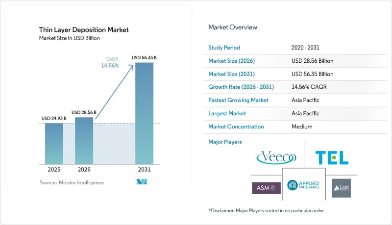
本報告按沉積技術(物理氣相沉積、化學氣相沉積等)、設備類型(線上生產線等)、沉積材料類型(金屬和合金、氧化物、氮化物和碳化物、化合物和2D材料)、終端應用產業(光學顯示器等)以及地區進行細分。市場預測以美元以金額為準。
全球薄膜沉積市場趨勢與洞察
晶片級 3D-IC 架構對超保形互連薄膜的需求日益成長。
異質整合正在改變互連設計,需要隔離層和籽晶層來覆蓋無空隙、高長寬比的通孔。台積電的CoWoS-S採用長寬比為20:1的矽穿孔堆疊邏輯電路和高頻寬記憶體,需要透過原子層沉積(ALD)沉積氮化鈦來控制銅擴散。英特爾2024年推出的Foveros Direct技術,由於其凸塊間距縮小至25μm,需改用鈷籽晶層,且階梯覆蓋率需達到95%,而化學氣相沉積(CVD)難以實現。三星晶圓代工廠的目標是在2027年實現2μm的線間距重新分佈,這將需要使用等離子體增強原子層沉積(PEALD)技術並配合釕襯墊。設備供應商的訂單激增,應用材料公司報告稱,其2024會計年度先進封裝沉積設備的銷售額年增了38%。該工業聯盟正在推廣引入新的前體,例如環戊二烯基釕,以實現低於300 度C且與有機中介層相容的製程。
鈣鈦礦串聯太陽能電池製造的快速規模化
鈣鈦礦矽疊層太陽能電池的轉換效率預計將在2024年突破33%,將帶動試點生產線的開發熱潮。牛津光電公司(Oxford Photovoltikes)已在勃蘭登堡啟動了200兆瓦的生產,該生產線採用狹縫式鈣鈦礦層與PECVD法製備的氧化錫電子傳輸膜相結合。隆基半導體(Longi)與邁耶·伯格公司(Meyer Burger)合作,計劃透過在其TOPCon組件中整合鈣鈦礦,在2026年實現30%的轉換效率。美國能源局已津貼4000萬美元用於一項太空原子層沉積(SALD)項目,旨在將鈍化層的產量提高十倍。創業投資也正源源不絕地湧入。 Swift Solar公司已籌集2,700萬美元,用於利用捲對捲濺鍍技術製備透明導電層的輕型疊層太陽能板的商業化。國際能源總署 (IEA) 預測,到 2030 年,串聯面板產能將達到 50 GW,前提是沉積單元的運轉率維持在 90% 以上,材料利用率超過 70%。
由於氦氣和高純度前驅體供應緊張,營運成本增加。
美國聯邦氦氣儲備的枯竭導致現貨價格從2023年的每立方公尺8美元飆升至2024年中期的每立方公尺16美元。一座300毫米晶圓廠每年消耗1500萬立方米氦氣,Lam Research公司透露,其在2024會計年度額外增加了1200萬美元的氦氣成本。閉合迴路回收系統可以回收95%的製程氣體,但每個系統的安裝成本高達300萬美元。高介電常數材料也面臨類似的短缺,目前只有三家公司生產四氯化鉿,導致前置作業時間從8週延長至20週。中國於2024年8月實施的鋯化合物出口限制進一步加劇了供應緊張,迫使晶圓廠簽署雙源協議,導致單位成本上漲18%。
細分市場分析
2025年,化學氣相沉積(CVD)在薄膜沉積市場佔據50.74%的市佔率。這反映了其在以高沉積速率沉積介電材料、多晶矽和鎢方面的多功能性。原子層沉積(ALD)預計將以17.18%的複合年成長率成長,這主要得益於對3nm以下電晶體閘極的需求,此類閘極需要埃級厚度控制。預計到2025年,ALD在薄膜沉積市場的規模將達到92億美元,並在2031年翻倍。物理氣相沉積(PVD)在成熟節點的鋁佈線領域仍佔據穩固地位,但像Lam Research的「SABRE 3D」這樣的混合製程將離子化PVD與ALD隔離層結合,可將界面電阻降低25%。聚合物分子層沉積(MLD)是一種新興技術,雖然仍處於早期階段,但它正在拓展軟性電子產品的功能選擇,並創造快速成長的收入來源。
邏輯晶片代工廠向環柵(GAA)奈米片過渡時,採用的原子層沉積(ALD)製程步驟多達15步,而上一代製程僅需8步。英特爾的18A節點標誌著這一飛躍,其結構中,氧化鉿和氮化鈦層包裹著長寬比。由於沉積速率高達100奈米/分鐘,化學氣相沉積(CVD)製程晶圓成本低,因此在淺溝槽絕緣(STI)和層間介質間隙填充方面仍佔據主導地位。隨著長寬比的增加,供應商正在開發高密度等離子體CVD和高回流焊接襯墊,以延緩這項過渡。選擇性沉積是一個活躍的研究領域,東京電子株式會社的「Tactras Vigus」系統結合了原子層沉積(ALD)和原子層光刻(ALE)以及原位測量技術,實現了±0.5奈米的自對準接觸,並有望在下一代邏輯晶片中省去微影術程。
預計到2025年,批量式原子層沉積爐將佔總銷售額的56.05%,這主要得益於其在通用邏輯、太陽能電池和光學塗層領域較低的單晶片成本。同時,卷對卷(R2R)和空間原子層沉積(ALD)設備預計將以16.36%的複合年成長率成長,這反映出市場正向需要連續卷式加工的軟性OLED顯示器、電池隔膜和雙面太陽能電池組件等領域轉變。單片晶圓叢集在先進邏輯和3D NAND領域仍然至關重要,因為透過真空整合腔室進行顆粒控制是關鍵。 2025年,太空原子層沉積設備的薄膜沉積市場規模為28億美元,但隨著產能問題的緩解,預計到2031年將達到60億美元。
貝納克(Beneq)的空間原子層沉積(ALD)運轉率超過85%,克服了大規模部署的傳統障礙。應用材料公司(Applied Materials)的「Olympia」平台將空間ALD和物理氣相沉積(PVD)模組整合到共用傳輸系統中,在TOPCon鈍化製程中實現了每小時1200片晶圓的生產速度,比間歇式反應器提高了15倍。馮·阿爾登公司(Von Aldenne)的捲對捲磁控濺射技術以20米/分鐘的速度在聚醯亞胺上沉積氧化銦鋅,從而能夠製造彎曲半徑為3毫米的折疊式智慧型手機。佳能安納瓦公司(Canon Anelva)的「ENAS」平台將機器學習技術整合到濺鍍輸出控制中,將300毫米晶圓上的薄膜厚度偏差降低到約1.5%,從而放寬了10奈米以下銅佈線製程窗口的限制。
區域分析
預計到2025年,亞太地區將佔全球銷售額的44.78%,主要得益於台積電、三星以及多家中國晶圓代工廠產能的擴張。該地區的資本支出將超過360億美元,其中台積電將佔據大部分,而台積電的支出中將有25%用於沉積設備。在中國,中芯國際14奈米生產線部署AMEC設備後,到2024年,其設備自給率將提升至28%。韓國政府將提供20兆韓元的補貼,支持SK海力士擴大HBM(氫溴酸硼)的量產規模,該公司已訂購120台ALD(原子層沉積)反應器。日本Rapidus Alliance將藉助IBM和IMEC的專業技術,採購30台設備用於端到端(Gate to Gate)技術研發。
在北美,隨著《晶片和半導體產業戰略法案》(CHIPS Act)的實施,復甦跡象正在顯現。英特爾和台積電鳳凰城工廠計畫在2026年安裝300多台反應器,而美光位於紐約的DRAM工廠計畫使用80台原子層沉積(ALD)設備進行電容器的介電層形成。應用材料公司已在蒙大拿州啟動一座價值40億美元的工廠建設,以滿足激增的需求,並新增20萬平方英尺的無塵室空間。歐洲正專注於功率半導體和化合物半導體。英飛凌位於德勒斯登的工廠和台積電的歐洲合資企業正在增設60台物理氣相沉積(PVD)和化學氣相沉積(CVD)設備,用於碳化矽和銅線材的生產。在中東,沙烏地阿拉伯20吉瓦的太陽能競標等大型企劃吸引了馮阿爾登和Singulus等公司訂購大面積濺射生產線,從而擴大了該地區的市場佔有率。南美和非洲仍在發展中,但間接受益於依賴亞洲製造能力的通用太陽能產品的進口。區域研究機構正在研究用於軟性感測器的捲對卷原子層沉積(ALD)技術,建立本地技術訣竅,這可能會在2030年以後略微提高設備銷售額。雖然這些新興地區目前的銷售額合計不到5%,但成本曲線的下降帶來了長期成長機會。
其他好處
- Excel格式的市場預測(ME)表
- 3個月的分析師支持
目錄
第1章:引言
- 研究假設和市場定義
- 調查範圍
第2章:調查方法
第3章執行摘要
第4章 市場狀況
- 市場概覽
- 市場促進因素
- 晶片級 3D-IC 架構對超保形互連薄膜的需求日益成長。
- 鈣鈦礦串聯太陽能電池製造製程的快速擴張
- 透過太空原子層沉積和捲對卷物理氣相沉積的技術突破,每奈米的成本顯著降低。
- 政府採取與 CHIPS 方法類似的獎勵,將導致國內沉澱設備的資本投資增加。
- 利用人工智慧進行預測性維護,減少儲存設備的運作
- 生物可分解植入塗層在醫療技術領域的出現
- 市場限制因素
- 由於氦氣和高純度前驅體供應緊張,營運成本增加。
- 將範圍 3 碳排放報告義務擴展至真空製程的缺點
- 真空製程領域熟練人員的短缺延長了製造工廠推出大規模生產所需的時間。
- 透過積層製造功能層實現競爭
- 宏觀經濟因素的影響
- 產業價值鏈分析
- 監理情勢
- 技術展望
- 波特五力分析
第5章 市場規模與成長預測
- 透過沉澱技術
- 物理氣相沉積(PVD)
- 化學氣相沉積(CVD)
- 原子層沉積(ALD)
- 混合和新興技術
- 依設備類型
- 批次處理系統
- 單晶圓叢集裝置
- 卷對卷/空間系統
- 線上生產線
- 依材料類型
- 金屬和合金
- 氧化物
- 氮化物和碳化物
- 化合物和2D材料
- 按最終用途行業分類
- 半導體和微電子
- 太陽能發電和儲能
- 醫療設備和醫療保健
- 光纖顯示器
- 工具和工業零件
- 按地區
- 北美洲
- 美國
- 加拿大
- 墨西哥
- 南美洲
- 巴西
- 阿根廷
- 其他南美國家
- 歐洲
- 德國
- 英國
- 法國
- 義大利
- 西班牙
- 俄羅斯
- 其他歐洲國家
- 亞太地區
- 中國
- 日本
- 印度
- 韓國
- 澳洲
- 其他亞太國家
- 中東和非洲
- 中東
- 沙烏地阿拉伯
- 阿拉伯聯合大公國
- 土耳其
- 其他中東國家
- 非洲
- 南非
- 奈及利亞
- 埃及
- 其他非洲地區
- 中東
- 北美洲
第6章 競爭情勢
- 市場集中度
- 策略趨勢
- 市佔率分析
- 公司簡介
- Applied Materials Inc.
- Lam Research Corporation
- Tokyo Electron Limited
- ASM International NV
- Veeco Instruments Inc.
- Aixtron SE
- Advanced Micro-Fabrication Equipment Inc.(AMEC)
- IHI Hauzer Techno Coating BV
- Oerlikon Balzers
- CVD Equipment Corporation
- Canon Anelva Corporation
- ULVAC Inc.
- Picosun Oy
- Beneq Group Oy
- Kurt J. Lesker Company
- Mustang Vacuum Systems LLC
- Optorun Co., Ltd.
- Von Ardenne GmbH
- Singulus Technologies AG
- Platit AG
第7章 市場機會與未來展望
According to Mordor Intelligence, the thin layer deposition market size was valued at USD 24.93 billion in 2025 and estimated to grow from USD 28.56 billion in 2026 to reach USD 56.35 billion by 2031, at a CAGR of 14.56% during the forecast period (2026-2031).
This report is Segmented by Deposition Technology (Physical Vapor Deposition, Chemical Vapor Deposition, and More), Equipment Type (In-Line Production Lines, and More), Material Type Deposited (Metals and Alloys, Oxides, Nitrides and Carbides, Compound and 2-D Materials), End-Use Industry (Optics and Displays, and More), and Geography. The Market Forecasts are Provided in Terms of Value in USD.
Global Thin Layer Deposition Market Trends and Insights
Chiplet And 3D-IC Architectures Intensify The Need For Ultra-Conformal Interconnect Films
Heterogeneous integration is changing interconnect design, demanding barrier and seed layers that cover high-aspect-ratio vias without voids. Taiwan Semiconductor Manufacturing Company's CoWoS-S stacks logic with high-bandwidth memory using 20:1 aspect-ratio through-silicon vias that require titanium nitride deposited by atomic layer deposition for copper diffusion control. Intel's 2024 Foveros Direct technology reduced bump pitch to 25 μm, forcing a shift to cobalt seed layers with 95% step coverage that chemical vapor deposition struggles to achieve. Samsung Foundry aims for 2 μm line-and-space redistribution by 2027, which will rely on plasma-enhanced atomic layer deposition of ruthenium liners. Tool vendors saw orders surge; Applied Materials reported 38% year-over-year growth in advanced-packaging deposition tools in fiscal 2024. Industry consortia are pushing new precursors, such as cyclopentadienyl-based ruthenium, to enable sub-300 °C processing compatible with organic interposers.
Rapid Scale-Up of Perovskite Tandem Solar Cell Manufacturing
Perovskite-silicon tandems surpassed the 33% efficiency mark in 2024, sparking a surge in the development of pilot lines. Oxford Photovoltaics commenced 200 MW production in Brandenburg, utilizing slot-die perovskite layers in combination with PECVD tin oxide electron transport films. Longi has partnered with Meyer Burger to integrate perovskites into TOPCon modules, aiming for 30% efficiency by 2026. The U.S. Department of Energy has granted USD 40 million to spatial atomic layer deposition projects, aiming for 10X throughput gains in passivation layers. Venture capital is flowing: Swift Solar raised USD 27 million to commercialize lightweight tandem panels that rely on roll-to-roll sputtered transparent conductors. The International Energy Agency forecasts 50 GW of tandem capacity by 2030, provided that deposition tools maintain uptime above 90% and material utilization exceeds 70%.
Helium And High-Purity Precursor Supply Crunch Inflates OPEX
The U.S. Federal Helium Reserve depletion drove spot prices from USD 8 m-3 in 2023 to USD 16 m-3 by mid-2024. A 300 mm fab consumes 15 million m3 annually, and Lam Research disclosed USD 12 million extra helium costs in fiscal 2024. Closed-loop recovery systems recapture 95% of process gas but cost USD 3 million per installation. High-k precursors face similar strain; hafnium tetrachloride capacity is restricted to three makers, stretching lead times from 8 to 20 weeks. China's August 2024 export controls on zirconium compounds further tightened the supply, prompting fabs to enter into dual-source agreements that increase unit costs by 18%.
Other drivers and restraints analyzed in the detailed report include:
- Spatial ALD And Roll-To-Roll PVD Breakthroughs Slashing Cost Per Nanometer
- Government CHIPS-Like Incentives Boosting Domestic Deposition Tool CAPEX
- Escalating Scope-3 Carbon-Reporting Mandates Penalize Vacuum Processes
For complete list of drivers and restraints, kindly check the Table Of Contents.
Segment Analysis
Chemical vapor deposition held a 50.74% market share in the thin layer deposition market in 2025, reflecting its versatility in depositing dielectrics, polysilicon, and tungsten at high rates. Atomic layer deposition is forecast to grow at a 17.18% CAGR, driven by the need for sub-3 nm transistor gates, which require angstrom-scale thickness control. The thin layer deposition market size allocated to ALD reached USD 9.2 billion in 2025 and is expected to double by 2031. Physical vapor deposition remains entrenched for aluminum interconnects at mature nodes; however, hybrid flows, such as Lam Research's SABRE 3D, merge ionized PVD with ALD barriers to reduce interface resistance by 25%. The emerging molecular layer deposition of polymers broadens the functional options for flexible electronics, adding a nascent but fast-growing revenue stream.
Logic foundries moving to gate-all-around nanosheets employ up to 15 ALD steps, versus eight in the prior generation. Intel's 18A node epitomizes this leap with hafnium oxide and titanium nitride stacks wrapped around channels with 5:1 aspect ratios. CVD maintains dominance in shallow trench isolation and inter-layer dielectric gap-fill because 100 nm min-1 rates keep wafer costs down. As aspect ratios increase, suppliers are advancing high-density plasma CVD and high-reflow liners to delay switchover points. Selective deposition is an active frontier: Tokyo Electron's Tactras Vigus tool combines ALE and ALD with in-situ metrology, achieving +-0.5 nm self-aligned contacts that could eliminate lithography steps in the next logic cycle.
Batch furnaces delivered 56.05% of 2025 revenue, prized for their low cost per wafer in commodity logic, solar, and optical coatings. However, roll-to-roll and spatial tools registered a 16.36% CAGR, reflecting a pivot toward flexible OLED displays, battery separators, and bifacial solar modules that need web-based continuous processing. Single-wafer clusters remain indispensable in advanced logic and 3D NAND, where vacuum-integrated chambers ensure particle control. The thin layer deposition market size for spatial ALD equipment was USD 2.8 billion in 2025 and is expected to reach USD 6 billion by 2031 as throughput concerns ease.
Beneq's spatial ALD uptime moved past 85% in 2024, removing a historical barrier to mass adoption. Applied Materials' Olympia integrates spatial ALD and PVD modules in a shared transfer system, achieving 1,200 wafers per hour for TOPCon passivation, a 15X productivity increase over batch reactors. Roll-to-roll magnetron sputtering at Von Ardenne coats indium zinc oxide on polyimide at a rate of 20 m min-1, enabling foldable phones with a bend radius of 3 mm. Canon Anelva's ENAS platform integrates machine learning into sputter power control, reducing thickness variation to around 1.5% on 300 mm wafers, thereby easing process windows for sub-10 nm copper interconnects.
Complete Report Scope:
- By Deposition Technology
- Physical Vapor Deposition (PVD)
- Chemical Vapor Deposition (CVD)
- Atomic Layer Deposition (ALD)
- Hybrid / Emerging Techniques
- By Equipment Type
- Batch Systems
- Single-wafer Cluster Tools
- Roll-to-Roll / Spatial Systems
- In-line Production Lines
- By Material Type Deposited
- Metals and Alloys
- Oxides
- Nitrides and Carbides
- Compound / 2-D Materials
- By End-Use Industry
- Semiconductors and Micro-electronics
- Photovoltaics and Energy Storage
- Medical Devices and Healthcare
- Optics and Displays
- Tools and Industrial Components
- By Geography
- North America
- United States
- Canada
- Mexico
- South America
- Brazil
- Argentina
- Rest of South America
- Europe
- Germany
- United Kingdom
- France
- Italy
- Spain
- Russia
- Rest of Europe
- Asia Pacific
- China
- Japan
- India
- South Korea
- Australia
- Rest of Asia Pacific
- Middle East and Africa
- Middle East
- Saudi Arabia
- United Arab Emirates
- Turkey
- Rest of Middle East
- Africa
- South Africa
- Nigeria
- Egypt
- Rest of Africa
- Middle East
- North America
Geography Analysis
The Asia Pacific region controlled 44.78% of 2025 revenue, driven by fabrication expansions at TSMC, Samsung, and multiple Chinese foundries. Capital spending in the region exceeded USD 36 billion, with TSMC alone accounting for a significant portion, 25% of which was earmarked for deposition equipment. China increased its equipment self-sufficiency to 28% in 2024, as AMEC tools were integrated into SMIC's 14 nm lines. South Korean subsidies of KRW 20 trillion supported SK Hynix's HBM ramps that ordered 120 ALD reactors. Japan's Rapidus alliance purchased 30 tools for gate-to-gate R&D, leveraging expertise from IBM and IMEC.
North America is rebounding under the CHIPS Act. Intel and TSMC Phoenix will install more than 300 reactors by 2026, while Micron's New York DRAM fab plans to use 80 ALD tools for capacitor dielectrics. Applied Materials broke ground on a USD 4 billion factory in Montana to serve this surge, adding 200,000 square feet of cleanrooms. Europe focuses on power and compound semiconductors; Infineon's Dresden fab and TSMC European JV add 60 PVD and CVD tools for silicon carbide and copper interconnects. Middle East solar mega-projects, such as Saudi Arabia's 20 GW tender, order large-area sputter lines from Von Ardenne and Singulus, thereby extending the regional share. South America and Africa remain nascent, but they benefit indirectly from commodity solar imports that rely on Asian manufacturing capacity. Regional research institutes explore roll-to-roll ALD for flexible sensors, building local know-how that could translate into modest equipment sales post-2030. Collectively, these emerging regions represent under 5% of current revenue, yet they provide a long tail of opportunity once cost curves fall.
- Applied Materials Inc.
- Lam Research Corporation
- Tokyo Electron Limited
- ASM International NV
- Veeco Instruments Inc.
- Aixtron SE
- Advanced Micro-Fabrication Equipment Inc. (AMEC)
- IHI Hauzer Techno Coating B.V.
- Oerlikon Balzers
- CVD Equipment Corporation
- Canon Anelva Corporation
- ULVAC Inc.
- Picosun Oy
- Beneq Group Oy
- Kurt J. Lesker Company
- Mustang Vacuum Systems LLC
- Optorun Co., Ltd.
- Von Ardenne GmbH
- Singulus Technologies AG
- Platit AG
Additional Benefits:
- The market estimate (ME) sheet in Excel format
- 3 months of analyst support
TABLE OF CONTENTS
1 INTRODUCTION
- 1.1 Study Assumptions and Market Definition
- 1.2 Scope of the Study
2 RESEARCH METHODOLOGY
3 EXECUTIVE SUMMARY
4 MARKET LANDSCAPE
- 4.1 Market Overview
- 4.2 Market Drivers
- 4.2.1 Chiplet And 3D-IC Architectures Intensify Need for Ultra-Conformal Interconnect Films
- 4.2.2 Rapid Scale-Up of Perovskite Tandem Solar Cell Manufacturing
- 4.2.3 Spatial ALD And Roll-To-Roll PVD Breakthroughs Slashing Cost / Nm
- 4.2.4 Government CHIPS-Like Incentives Boosting Domestic Deposition Tool CAPEX
- 4.2.5 AI-Powered Predictive Maintenance Reducing Deposition Tool Downtime
- 4.2.6 Emergence Of Biodegradable Implant Coatings in Med-Tech
- 4.3 Market Restraints
- 4.3.1 Helium And High-Purity Precursor Supply Crunch Inflates OPEX
- 4.3.2 Escalating Scope-3 Carbon-Reporting Mandates Penalise Vacuum Processes
- 4.3.3 Skilled Vacuum-Process Talent Shortage Lengthens Fab Ramps
- 4.3.4 Competition From Additive Manufacturing of Functional Layers
- 4.4 Impact of Macroeconomic Factors
- 4.5 Industry Value Chain Analysis
- 4.6 Regulatory Landscape
- 4.7 Technological Outlook
- 4.8 Porter's Five Forces Analysis
- 4.8.1 Bargaining Power of Buyers
- 4.8.2 Bargaining Power of Suppliers
- 4.8.3 Threat of New Entrants
- 4.8.4 Threat of Substitute Products
- 4.8.5 Intensity of Competitive Rivalry
5 MARKET SIZE AND GROWTH FORECASTS (VALUE)
- 5.1 By Deposition Technology
- 5.1.1 Physical Vapor Deposition (PVD)
- 5.1.2 Chemical Vapor Deposition (CVD)
- 5.1.3 Atomic Layer Deposition (ALD)
- 5.1.4 Hybrid / Emerging Techniques
- 5.2 By Equipment Type
- 5.2.1 Batch Systems
- 5.2.2 Single-wafer Cluster Tools
- 5.2.3 Roll-to-Roll / Spatial Systems
- 5.2.4 In-line Production Lines
- 5.3 By Material Type Deposited
- 5.3.1 Metals and Alloys
- 5.3.2 Oxides
- 5.3.3 Nitrides and Carbides
- 5.3.4 Compound / 2-D Materials
- 5.4 By End-Use Industry
- 5.4.1 Semiconductors and Micro-electronics
- 5.4.2 Photovoltaics and Energy Storage
- 5.4.3 Medical Devices and Healthcare
- 5.4.4 Optics and Displays
- 5.4.5 Tools and Industrial Components
- 5.5 By Geography
- 5.5.1 North America
- 5.5.1.1 United States
- 5.5.1.2 Canada
- 5.5.1.3 Mexico
- 5.5.2 South America
- 5.5.2.1 Brazil
- 5.5.2.2 Argentina
- 5.5.2.3 Rest of South America
- 5.5.3 Europe
- 5.5.3.1 Germany
- 5.5.3.2 United Kingdom
- 5.5.3.3 France
- 5.5.3.4 Italy
- 5.5.3.5 Spain
- 5.5.3.6 Russia
- 5.5.3.7 Rest of Europe
- 5.5.4 Asia Pacific
- 5.5.4.1 China
- 5.5.4.2 Japan
- 5.5.4.3 India
- 5.5.4.4 South Korea
- 5.5.4.5 Australia
- 5.5.4.6 Rest of Asia Pacific
- 5.5.5 Middle East and Africa
- 5.5.5.1 Middle East
- 5.5.5.1.1 Saudi Arabia
- 5.5.5.1.2 United Arab Emirates
- 5.5.5.1.3 Turkey
- 5.5.5.1.4 Rest of Middle East
- 5.5.5.2 Africa
- 5.5.5.2.1 South Africa
- 5.5.5.2.2 Nigeria
- 5.5.5.2.3 Egypt
- 5.5.5.2.4 Rest of Africa
- 5.5.5.1 Middle East
- 5.5.1 North America
6 COMPETITIVE LANDSCAPE
- 6.1 Market Concentration
- 6.2 Strategic Moves
- 6.3 Market Share Analysis
- 6.4 Company Profiles (includes Global level Overview, Market level overview, Core Segments, Financials as available, Strategic Information, Market Rank/Share for key companies, Products and Services, and Recent Developments)
- 6.4.1 Applied Materials Inc.
- 6.4.2 Lam Research Corporation
- 6.4.3 Tokyo Electron Limited
- 6.4.4 ASM International NV
- 6.4.5 Veeco Instruments Inc.
- 6.4.6 Aixtron SE
- 6.4.7 Advanced Micro-Fabrication Equipment Inc. (AMEC)
- 6.4.8 IHI Hauzer Techno Coating B.V.
- 6.4.9 Oerlikon Balzers
- 6.4.10 CVD Equipment Corporation
- 6.4.11 Canon Anelva Corporation
- 6.4.12 ULVAC Inc.
- 6.4.13 Picosun Oy
- 6.4.14 Beneq Group Oy
- 6.4.15 Kurt J. Lesker Company
- 6.4.16 Mustang Vacuum Systems LLC
- 6.4.17 Optorun Co., Ltd.
- 6.4.18 Von Ardenne GmbH
- 6.4.19 Singulus Technologies AG
- 6.4.20 Platit AG
7 MARKET OPPORTUNITIES AND FUTURE OUTLOOK
- 7.1 White-space and Unmet-need Assessment

 沉澱設備市場-2026-2032年全球市場預測
 先進薄膜沉積市場預測至2034年—按沉積技術、材料類型、製程模式、應用、產業和地區分類的全球分析
 薄膜形成:趨勢、關鍵問題與市場分析
 薄膜半導體沉積市場機會、成長要素、產業趨勢分析及2026-2035年預測。薄膜沉積設備市場:依技術、材料、設備類型、應用和終端用戶產業分類,全球預測,2026-2032年離子布植設備市場:依晶圓尺寸、產品類型、能量範圍、離子源類型和最終用途產業分類-全球預測,2026-2032年
 薄膜沉積設備市場-2025-2030年預測外延沉積市場:預測(2025-2030 年)
 薄膜半導體沉積:全球市場佔有率和排名、總收入和需求預測(2025-2031年)