

 |
市場調查報告書
商品編碼
2083345
薄膜半導體沉積市場機會、成長要素、產業趨勢分析及2026-2035年預測。Thin Film Semiconductor Deposition Market Opportunity, Growth Drivers, Industry Trend Analysis, and Forecast 2026 - 2035 |
||||||

全球薄膜半導體沉積市場預計到 2025 年價值為 348 億美元,預計到 2035 年將以 7.7% 的複合年成長率成長至 775 億美元。
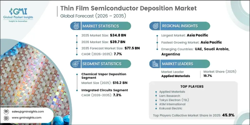
這一成長主要得益於人工智慧 (AI) 工作負載的快速擴張、政府主導的半導體自給自足計劃,以及向依賴超精密原子級薄膜沉積的先進製程節點加速轉型。需求日益集中在最先進的邏輯和記憶體製造領域,在這些領域,化學、物理和原子層沉積 (ALD) 技術直接影響著 5 奈米以下微結構的良率。人工智慧加速器、汽車電子、先進記憶體架構和下一代可再生能源設備等各種終端應用的採用,也支撐著市場發展,並增強了多個產業的需求基礎。超大規模資料中心的日益部署和雲端基礎設施的擴展進一步增加了對高效能晶片的需求。這些晶片在製造過程中都需要多次沉積循環。此外,最新的記憶體技術,例如先進的 3D NAND,採用 200 層或更多層的堆疊結構,需要重複的沉積和蝕刻製程來維持每一層的結構精度。隨著製程變得越來越複雜,每片晶圓所使用的設備數量不斷增加,進一步增強了整個半導體沉積生態系的長期需求前景。
| 市場範圍 | |
|---|---|
| 開始年份 | 2025 |
| 預測期 | 2026-2035 |
| 上市時的市場規模 | 348億美元 |
| 預計金額 | 775億美元 |
| 複合年成長率 | 7.7% |
預計到2025年,化學氣相沉積(CVD)領域的銷售額將達到162億美元。其市場主導地位得益於廣泛的應用,包括介電層、導電填料、阻擋塗層以及跨越多個半導體節點的高密度等離子體製程。在成熟和先進製造環境中,CVD技術的積極應用進一步鞏固了其在裝置製造中的關鍵作用。
預計到2025年,積體電路(IC)市場規模將達到251億美元,佔市場佔有率的72%。 IC製造中的薄膜沉積製程包括介電層形成、絕緣層形成和金屬化結構,這些構成了半導體生產的基礎。先進邏輯和高密度記憶體架構的需求尤其強勁,這些架構的設計複雜性不斷增加,導致每個晶片的沉積強度顯著提高。
預計2025年,北美薄膜半導體沉積市場規模將達108億美元,市佔率將達31.1%。該地區的成長主要集中在美國,這得益於大規模的政策舉措以及私營企業在多個州擴建半導體製造設施,從而增強了國內產能和供應鏈韌性。
競爭格局包括應用材料公司 (Applied Materials)、Lam Research、東京電子 (Tokyo Electron)、ASM International、國際電氣株式會社 (Kokusai Electric Co., Ltd.)、NAURA Technology Group、Vico Instruments、Aixtron、SVT Associates、Semicore Equipment、Den Technology Group、Vico Instruments、Aixtron、SVT Associates、Semicore Equipment、Den Technology Ecuum、Rauments ZLD Technology 等主要設備和技術供應商。薄膜半導體沉積市場的企業正透過持續投資於下一代沉積技術來鞏固其市場地位,這些技術能夠提高原子級精度和製程均勻性。許多公司正在擴展產品系列,以滿足諸如 5nm 以下和高長寬比3D 架構等先進節點的需求,在這些節點上,製程控制變得日益重要。與半導體晶圓廠和代工廠建立戰略合作夥伴關係是優先事項,以確保長期設備供應合約和聯合開發項目。此外,製造商正致力於自動化、人工智慧驅動的製程控制和預測性維護功能,以減少停機時間並提高良率。
目錄
第1章:調查方法和範圍
第2章執行摘要
第3章 行業洞察
- 產業生態系分析
- 影響產業的因素
- 促進因素
- 對人工智慧和高效能運算晶片的需求不斷成長
- 半導體裝置的持續小型化
- 全球半導體製造設施的擴張
- 擴大先進記憶體和功率半導體的生產
- 產業潛在風險與挑戰
- 薄膜沉積設備的高資本投資與營運成本
- 半導體製造技術的快速發展
- 市場機遇
- 先進包裝技術的應用日益廣泛
- 化合物半導體和新興材料的應用日益廣泛
- 促進因素
- 成長潛力分析
- 監理情勢
- 技術展望
- 最新科技趨勢
- 新興技術
- 價格趨勢分析
- 未來市場趨勢
- 專利分析
- 波特的分析
- PESTLE分析
- 人工智慧和生成式人工智慧對市場的影響
- 價值鏈分析
- 投資與資金籌措分析
- 消費者洞察
第4章 競爭情勢
- 介紹
- 企業市佔率分析:按地區分類
- 北美洲
- 歐洲
- 亞太地區
- 中東和非洲
- 拉丁美洲
- 主要進展
- 主要夥伴關係和聯盟
- 主要併購活動
- 產品創新和新產品發布
- 市場擴大策略
- 競爭定位矩陣
第5章 市場規模及預測:依薄膜沉積技術分類,2022-2035年
- 化學氣相沉積(CVD)
- 大氣壓力化學氣相沉積(APCVD)
- 低壓化學氣相沉積(LPCVD)
- 血漿增強型心血管疾病(PECVD)
- 其他心血管疾病治療方法
- 物理氣相沉積(PVD)
- 濺射
- 蒸發法
- 其他PVD技術
- 原子層沉積(ALD)
- 其他
第6章 市場規模與預測:依應用領域分類,2022-2035年
- 積體電路(IC)
- 微處理器
- 儲存設備(DRAM、NAND、NOR)
- 其他
- 光電子和顯示裝置
- LED顯示器
- OLED面板
- 液晶螢幕
- 其他
- 太陽能電池/光伏發電
- 薄膜太陽能板
- 晶體矽太陽能電池
- 其他
- 微機電系統和感測器
- 壓力感測器
- 慣性感測器(加速計、陀螺儀)
- 光學感測器
- 其他
- 其他
第7章 市場規模與預測:依最終用戶分類,2022-2035年
- 家用電子產品
- 智慧型手機和平板電腦
- 筆記型電腦和計算設備
- 其他
- 車
- 電動車(EV)與電池管理系統
- 高級駕駛輔助系統(ADAS)
- 其他
- 能源與電力
- 太陽能發電系統
- 電力電子和變換器
- 其他
- 航太/國防
- 軍事電子通訊系統
- 航太零件和航空電子設備
- 其他
- 通訊與科技
- 通訊基礎設施
- 資料中心和雲端運算
- 其他
第8章 市場規模及預測:依地區分類,2022-2035年
- 北美洲
- 美國
- 加拿大
- 歐洲
- 德國
- 法國
- 英國
- 荷蘭
- 西班牙
- 義大利
- 亞太地區
- 中國
- 日本
- 韓國
- 印度
- 澳洲
- 中東和非洲
- 沙烏地阿拉伯
- UAE
- 南非
- 拉丁美洲
- 巴西
- 阿根廷
- 墨西哥
第9章:公司簡介
- Applied Materials Inc.
- Lam Research Corporation
- Tokyo Electron Limited(TEL)
- ASM International NV
- Kokusai Electric Corporation
- NAURA Technology Group
- Veeco Instruments Inc.
- Aixtron SE
- SVTA(SVT Associates)
- Semicore Equipment Inc.
- Denton Vacuum
- PSR Semi
- KDF Electronic & Vacuum Services
- Yunmao Technology
- ZLD Technology
The Global Thin Film Semiconductor Deposition Market was valued at USD 34.8 billion in 2025 and is estimated to grow at a CAGR of 7.7% to reach USD 77.5 billion by 2035.
Growth is reinforced by the rapid expansion of artificial intelligence workloads, government-led semiconductor sovereignty programs, and the accelerating shift toward advanced process nodes that depend on ultra-precise atomic-level film deposition. Demand is increasingly concentrated in leading-edge logic and memory manufacturing, where chemical, physical, and atomic layer deposition techniques directly influence yield performance at sub-5nm geometries. The market is also supported by diversified end-use adoption across AI accelerators, automotive electronics, advanced memory architectures, and next-generation renewable energy devices, reinforcing a multi-industry demand base. Rising hyperscale data center deployment and cloud infrastructure expansion are further intensifying the requirement for high-performance chips, each of which requires multiple deposition cycles during fabrication. In addition, modern memory technologies such as advanced 3D NAND now involve more than 200 stacked layers, with each layer requiring repeated deposition and etching steps to maintain structural precision. This increasing process complexity continues to elevate equipment intensity per wafer, strengthening long-term demand visibility across the semiconductor deposition ecosystem.
| Market Scope | |
|---|---|
| Start Year | 2025 |
| Forecast Year | 2026-2035 |
| Start Value | $34.8 Billion |
| Forecast Value | $77.5 Billion |
| CAGR | 7.7% |
The chemical vapor deposition segment generated USD 16.2 billion in 2025. Its dominance is supported by broad applicability across dielectric layers, conductive fills, barrier coatings, and high-density plasma processes across multiple semiconductor nodes. Strong adoption across both mature and advanced fabrication environments continues to reinforce its critical role in device manufacturing.
The integrated circuits segment accounted for USD 25.1 billion in 2025, representing 72% share. Deposition steps across IC manufacturing include dielectric formation, insulation layers, and metallization structures form the backbone of semiconductor production. Demand is particularly strong in advanced logic and high-density memory architectures, where escalating design complexity requires significantly higher deposition intensity per chip.
North America Thin Film Semiconductor Deposition Market accounted for USD 10.8 billion in 2025, capturing 31.1% share. Growth in the region is strongly centered in the United States, supported by large-scale policy initiatives and private sector expansion of semiconductor fabrication facilities across multiple states, strengthening domestic production capacity and supply chain resilience.
The competitive landscape includes leading equipment and technology providers such as Applied Materials Inc., Lam Research Corporation, Tokyo Electron Limited, ASM International N.V., Kokusai Electric Corporation, NAURA Technology Group, Veeco Instruments Inc., Aixtron SE, SVT Associates, Semicore Equipment Inc., Denton Vacuum, PSR Semi, KDF Electronic & Vacuum Services, Yunmao Technology, and ZLD Technology. Companies in the thin film semiconductor deposition market are strengthening their position through continuous investment in next-generation deposition technologies that improve atomic-level precision and process uniformity. Many firms are expanding product portfolios to support advanced nodes such as sub-5nm and high-aspect-ratio 3D architectures, where process control is increasingly critical. Strategic partnerships with semiconductor fabs and foundries are being prioritized to secure long-term equipment supply agreements and co-development programs. Manufacturers are also focusing on automation, AI-driven process control, and predictive maintenance capabilities to reduce downtime and improve yield performance.
Table of Contents
Chapter 1 Methodology & Scope
- 1.1 Research approach
- 1.2 Quality commitments
- 1.2.1 GMI AI policy & data integrity commitment
- 1.2.1.1 Source consistency protocol
- 1.2.1 GMI AI policy & data integrity commitment
- 1.3 Research trail & confidence scoring
- 1.3.1 Research trail components
- 1.3.2 Scoring components
- 1.4 Data collection
- 1.4.1 Partial list of primary sources
- 1.5 Data mining sources
- 1.5.1 Paid sources
- 1.5.1.1 Sources, by region
- 1.5.1 Paid sources
- 1.6 Base estimates and calculations
- 1.6.1 Base year calculation for any one approach
- 1.7 Market estimates & forecasts parameters
- 1.8 Forecast model
- 1.8.1 Quantified market impact analysis
- 1.8.1.1 Mathematical impact of growth parameters on forecast
- 1.8.1 Quantified market impact analysis
- 1.9 Research transparency addendum
- 1.9.1 Source attribution framework
- 1.9.2 Quality assurance metrics
- 1.9.3 Our commitment to trust
- 1.10 Market definitions
Chapter 2 Executive Summary
- 2.1 Industry synopsis, 2022 - 2035
- 2.1.1 Deposition Technology trends
- 2.1.2 Application trends
- 2.1.3 End use trends
- 2.1.4 Regional trends
Chapter 3 Industry Insights
- 3.1 Industry ecosystem analysis
- 3.2 Industry impact forces
- 3.2.1 Growth drivers
- 3.2.1.1 Rising Demand for AI and High-Performance Computing Chips
- 3.2.1.2 Continuous Miniaturization of Semiconductor Devices
- 3.2.1.3 Expansion of Global Semiconductor Manufacturing Facilities
- 3.2.1.4 Increasing Production of Advanced Memory and Power Semiconductors
- 3.2.2 Industry pitfalls and challenges
- 3.2.2.1 High Capital and Operational Costs of Deposition Equipment
- 3.2.2.2 Rapid Technological Evolution in Semiconductor Manufacturing
- 3.2.3 Market opportunities
- 3.2.3.1 Growing Adoption of Advanced Packaging Technologies
- 3.2.3.2 Expanding Use of Compound Semiconductors and Emerging Materials
- 3.2.1 Growth drivers
- 3.3 Growth potential analysis
- 3.4 Regulatory landscape (Driven by primary research)
- 3.4.1 North America
- 3.4.2 Europe
- 3.4.3 Asia Pacific
- 3.4.4 Latin America
- 3.4.5 MEA
- 3.5 Technology landscape
- 3.5.1 Current technological trends
- 3.5.2 Emerging technologies
- 3.6 Pricing trend analysis (Driven by primary research)
- 3.7 Future market trends
- 3.8 Patent analysis
- 3.9 Porter's analysis
- 3.10 PESTEL analysis
- 3.11 Impact of AI and Generative AI on the market (Driven by primary research)
- 3.12 Value chain analysis (Driven by primary research)
- 3.13 Investment & funding analysis (Driven by primary research)
- 3.14 Consumer insights (Driven by primary research)
Chapter 4 Competitive Landscape, 2025
- 4.1 Introduction
- 4.2 Company market share analysis, by region, 2025
- 4.2.1 North America
- 4.2.2 Europe
- 4.2.3 Asia Pacific
- 4.2.4 Middle East & Africa
- 4.2.5 Latin America
- 4.3 Key developments
- 4.3.1 Key partnerships & collaborations
- 4.3.2 Major M&A activities
- 4.3.3 Product innovations & launches
- 4.3.4 Market expansion strategies
- 4.4 Competitive positioning matrix
Chapter 5 Market Size and Forecast, By Deposition Technology, 2022 - 2035 (USD Million)
- 5.1 Key trends
- 5.2 Chemical Vapor Deposition (CVD)
- 5.2.1 Atmospheric Pressure CVD (APCVD)
- 5.2.2 Low Pressure CVD (LPCVD)
- 5.2.3 Plasma Enhanced CVD (PECVD)
- 5.2.4 Other CVD Variants
- 5.3 Physical Vapor Deposition (PVD)
- 5.3.1 Sputtering
- 5.3.2 Evaporation
- 5.3.3 Other PVD Techniques
- 5.4 Atomic Layer Deposition (ALD)
- 5.5 Others
Chapter 6 Market Size and Forecast, By Application, 2022 - 2035 (USD Million)
- 6.1 Key trends
- 6.2 Integrated Circuits (ICs)
- 6.2.1 Microprocessors
- 6.2.2 Memory Devices (DRAM, NAND, NOR)
- 6.2.3 Others
- 6.3 Optoelectronics & Display Devices
- 6.3.1 LED Displays
- 6.3.2 OLED Panels
- 6.3.3 LCD Screens
- 6.3.4 Others
- 6.4 Solar Cells/Photovoltaics
- 6.4.1 Thin Film Solar Panels
- 6.4.2 Crystalline Silicon Solar Cells
- 6.4.3 Others
- 6.5 MEMS & Sensors
- 6.5.1 Pressure Sensors
- 6.5.2 Inertial Sensors (Accelerometers, Gyroscopes)
- 6.5.3 Optical Sensors
- 6.5.4 Others
- 6.6 Others
Chapter 7 Market Size and Forecast, By End User, 2022 - 2035 (USD Million)
- 7.1 Key trends
- 7.2 Consumer Electronics
- 7.2.1 Smartphones & Tablets
- 7.2.2 Laptops & Computing Devices
- 7.2.3 Others
- 7.3 Automotive
- 7.3.1 Electric Vehicles (EVs) & Battery Management Systems
- 7.3.2 Advanced Driver Assistance Systems (ADAS)
- 7.3.3 Others
- 7.4 Energy & Power
- 7.4.1 Solar Energy Systems
- 7.4.2 Power Electronics & Converters
- 7.4.3 Others
- 7.5 Aerospace & Defense
- 7.5.1 Military Electronics & Communication Systems
- 7.5.2 Aerospace Components & Avionics
- 7.5.3 Others
- 7.6 Communication & Technology
- 7.6.1 Telecommunications Infrastructure
- 7.6.2 Data Centers & Cloud Computing
- 7.6.3 Others
Chapter 8 Market Size and Forecast, By Region, 2022 - 2035 (USD Million)
- 8.1 Key trends
- 8.2 North America
- 8.2.1 U.S.
- 8.2.2 Canada
- 8.3 Europe
- 8.3.1 Germany
- 8.3.2 France
- 8.3.3 UK
- 8.3.4 Netherlands
- 8.3.5 Spain
- 8.3.6 Italy
- 8.4 Asia Pacific
- 8.4.1 China
- 8.4.2 Japan
- 8.4.3 South Korea
- 8.4.4 India
- 8.4.5 Australia
- 8.5 Middle East & Africa
- 8.5.1 Saudi Arabia
- 8.5.2 UAE
- 8.5.3 South Africa
- 8.6 Latin America
- 8.6.1 Brazil
- 8.6.2 Argentina
- 8.6.3 Mexico
Chapter 9 Company Profiles
- 9.1 Applied Materials Inc.
- 9.2 Lam Research Corporation
- 9.3 Tokyo Electron Limited (TEL)
- 9.4 ASM International N.V.
- 9.5 Kokusai Electric Corporation
- 9.6 NAURA Technology Group
- 9.7 Veeco Instruments Inc.
- 9.8 Aixtron SE
- 9.9 SVTA (SVT Associates)
- 9.10 Semicore Equipment Inc.
- 9.11 Denton Vacuum
- 9.12 PSR Semi
- 9.13 KDF Electronic & Vacuum Services
- 9.14 Yunmao Technology
- 9.15 ZLD Technology

 薄膜形成:趨勢、關鍵問題與市場分析
 沉澱設備市場:2026-2032年全球市場預測(依設備類型、技術類型、材料類型、系統配置及最終用途分類)薄膜沉積設備市場:依技術、材料、設備類型、應用和終端用戶產業分類,全球預測,2026-2032年離子布植設備市場:依晶圓尺寸、產品類型、能量範圍、離子源類型和最終用途產業分類-全球預測,2026-2032年
 薄膜沉積設備市場-2025-2030年預測外延沉積市場:預測(2025-2030 年)
 薄膜半導體沉積:全球市場佔有率和排名、總收入和需求預測(2025-2031年)薄層累積設備的全球市場規模:各產品,各用途,各地區,範圍及預測