


 |
市場調查報告書
商品編碼
2114334
原子層沉積:市場佔有率分析、產業趨勢與統計、成長預測(2026-2031)Atomic Layer Deposition - Market Share Analysis, Industry Trends & Statistics, Growth Forecasts (2026 - 2031) |
||||||

※ 本網頁內容可能與最新版本有所差異。詳細情況請與我們聯繫。
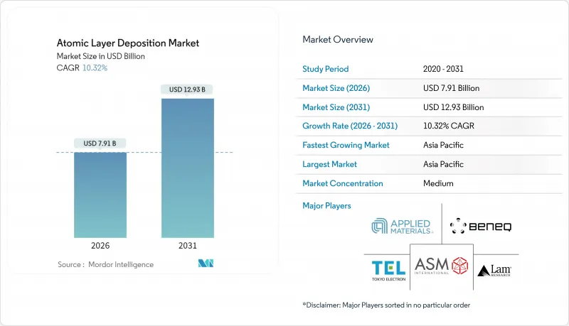
根據 Mordor Intelligence 預測,原子層沉積 (ALD) 市場規模預計將在 2026 年達到 79.1 億美元,到 2031 年將擴大到 129.3 億美元,預測期內複合年成長率為 10.32%。
本報告按設備類型(熱原子層沉積批次、等離子體增強原子層沉積等)、反應器配置(叢集單晶圓、獨立批次)、基板尺寸(200mm以下、300mm及其他)、薄膜沉積化學(氧化物、金屬及其他)、應用(半導體邏輯和記憶體、先進封裝等)以及地區進行細分。市場預測以美元計價。
全球原子層沉積(ALD)市場趨勢及洞察
亞洲3D NAND和DRAM節點小型化進程迅速推進
到2025年,隨著垂直NAND快閃記憶體層數超過300層,長寬比超過80:1,記憶體工廠將被迫在每片晶圓上實施多達14道ALD工藝,以保持側壁的一致性。 DRAM製造商也轉向電容直徑小於18奈米的1BETA結構。只有採用ALD製程製備的摻鋯氧化鉿才能在不發生洩漏的情況下填充這種微結構。三星透露,到2025年,ALD設備將佔其記憶體工廠資本投資的22%,高於三年前的16%。中國的長江儲存(YMTC)也緊隨其後,在其Xtacking 4.0設計中增加了ALD氮化鈦襯墊,並為每條月產能10萬片晶圓的生產線額外投資1.2億美元。這些投資鞏固了在亞太地區的領先地位,並進一步明確了至少未來兩代節點小型化技術對設備的需求前景。
向全環閘極 (GAA) 和高介電常數金屬閘極邏輯的過渡
環柵場場效電晶體(GAA)將通道封裝在共形高介電常數材料中,從而將等效氧化層厚度減小到0.7奈米以下。台積電的N2風險生產流程需要在12個循環的氧化鉿原子層沉積(ALD)堆疊層之後沉積氮化鈦功函數金屬,所有沉積過程均在獨立的ALD腔室中進行,以抑制氧串擾。英特爾的18A節點增加了選擇性ALD鈷襯墊層,可將接觸電阻降低19%。三星的第二代3奈米製程透過最佳化ALD化學成分來減薄界面層,從而實現了23%的功耗降低。雖然ALD循環時間最長可達180秒,但代工廠正在透過並行運轉腔室來緩解瓶頸,凸顯了ALD在3奈米以下邏輯裝置中的關鍵作用。
前驅體金屬供不應求與價格波動
釕、銥和鈷主要產自南非和俄羅斯,是鉑族金屬的產物,其供應受地緣政治風險影響。由於原子層沉積(ALD)和電解槽製造商競相爭奪有限的產能,釕的價格已從2024年的每金衡盎司450美元上漲至2025年底的每金衡盎司603美元。晶圓代工廠透過最佳化脈衝時序降低了釕的使用量,但隨著晶圓產量的持續成長,需求成長速度仍超過了效率提升所帶來的效益。目前正在測試替代化學成分,但認證週期需要2-3年,延長了企業受現貨價格波動的影響。
細分市場分析
到2025年,等離子體增強型設備將佔銷售額的38.23%,這反映了其在保護線路和化合物半導體方面卓越的低溫處理能力。由於奈米片邏輯和3D DRAM的製造需要低於300 度C的低溫處理,預計到2031年,等離子體系統的原子層沉積(ALD)市場將以近10%的複合年成長率成長,與整體市場趨勢一致。熱ALD無法以合理速度形成保形氮化物和鈦薄膜,而這正是該市場需求的基礎。相較之下,空間結構(尤其是在軟式電路板上)預計將以12.41%的複合年成長率成長,這需要在原子級精度和線速度之間進行權衡。 WCS 500平台每小時可塗覆10平方公尺的薄膜,使顯示器生產線能夠實現先前使用批量腔室無法達到的週期時間目標。然而,其前驅體廢料仍高出40%。熱批量處理系統仍然用於學術機構和生物醫學領域的生產線,因為在這些領域,等離子體損傷是不可接受的,但隨著晶圓廠整合到叢集設計中,其市場佔有率正在逐年萎縮。
展望未來,將等離子體原子層沉積(ALD)和原子層蝕刻(ALE)技術整合於同一包裝內的混合堆疊結構正吸引著人們的注意。東京電子的「Tactras」系統與單一模組相比,減少了晶圓交接次數,並將整體生產效率提高了18%。隨著晶圓廠對精度和產能的雙重追求,掌握此類整合技術的供應商將進一步擴大市場佔有率。同時,電池和顯示器製造商要求供應商提供卷對卷設計,以一半的成本實現與批量生產方法相同的均勻性,這表明原子層沉積市場的產品藍圖正在分化。
預計到2025年,叢集式單晶圓平台將佔銷售額的44.57%,維持11.02%的複合年成長率,主要得益於邏輯晶圓廠對污染隔離技術的投入。由於每片晶圓都佔據一個獨立的腔室,因此可以快速改變化學成分而不會產生串擾,這在交替形成鈷襯層和介電層時至關重要。原子層沉積中批量反應器的市佔率正在下降。這是因為,即使其單片成本更低,但7奈米以下節點的製程配方柔軟性限制仍然無法彌補。儘管如此,到2025年,批量設備仍將佔中國老一代晶圓廠新部署設備的38%,這顯示在尖端邏輯半導體之外,資本效率仍是一個決定性因素。
空間單晶圓系統透過結合污染控制和高機械吞吐量,模糊了傳統系統與空間單晶圓系統的界限。如果薄膜均勻性問題得到解決,叢集設備目前享有的溢價可能會受到衝擊。因此,供應商正在分散風險。 ASM International 的 Pulsar 系列在單晶圓領域保持領先地位,而其新的空間產品組合則瞄準了顯示器和電池用戶。未來十年,買家的選擇將取決於設備製造商能否在單一模組化框架內協調週期時間、薄膜品質和整體擁有成本。
區域分析
預計到2025年,亞太地區將維持53.43%的銷售額佔有率,並在2031年之前以11.28%的複合年成長率成長。台灣、韓國和中國大陸合計佔300毫米晶圓產能的78%,設備製造商東京電子和日立高新技術公司提供的在地採購供應鏈加速了該地區的普及。韓國在3D NAND領域的領先地位推動了對字線勢壘層和電荷設陷層的需求,而中國晶圓廠的擴張則吸收了成熟節點、影像感測器和電源管理積體電路所需的設備。日本受益於設備出口和固態電池線的早期部署。印度100億美元的半導體激勵計畫尚未促成大規模生產晶圓廠的建設,但顯示其具有長期需求潛力。
北美位居第二,這得益於《晶片技術創新與應用法案》(CHIPS Act)提供的390億美元撥款,以及英特爾、台積電、三星和美光宣布的超過2000億美元的晶圓廠投資。在這些項目中,原子層沉積(ALD)設備約佔晶圓廠設備總預算的14%。加拿大主要專注於研發,而墨西哥則專注於使用ALD技術製造銅擴散阻擋層的先進封裝生產線。
在430億歐元(470億美元)的歐盟晶片法案的支持下,歐洲半導體產業持續發展。該法案旨在2030年佔據全球半導體市場20%的佔有率。英特爾位於馬格德堡的工廠和台積電位於德勒斯登的工廠計畫從2026年起開始量產原子層沉積(ALD)模組。意法半導體正在擴大其位於克洛爾的業務,為汽車行業的客戶提供採用ALD製程保護的碳化矽裝置。中東和非洲地區仍處於發展階段,相關項目僅限於投資基金所進行的試點計畫。
在南美洲,市場進入僅限於學術研究機構,工業資本投資也更著重於組裝而非前端製造。因此,原子層沉積(ALD)市場仍然高度集中,預計到2025年,排名前五的國家——台灣、韓國、中國、美國和日本——將佔據設備銷售額的84%。儘管補貼可能會對市場結構造成輕微影響,但成熟的技術訣竅、完善的供應商生態系統以及現有的折舊免稅額機制很可能在可預見的未來繼續保持亞太地區的主導地位。
其他好處:
- Excel格式的市場預測(ME)表
- 3個月的分析師支持
目錄
第1章:引言
- 研究假設和市場定義
- 調查範圍
第2章:調查方法
第3章執行摘要
第4章 市場狀況
- 市場概覽
- 市場促進因素
- 亞洲3D NAND和DRAM節點小型化技術快速發展
- 向全環閘極 (GAA) 和高介電常數金屬閘極邏輯的過渡
- 迷你/微型LED背板的快速普及
- 電動汽車電池對固體電解質塗層的需求
- 利用奈米塗層改善醫療植入的生物相容性
- 政府資助的試驗生產線投資、歐盟晶片法、《晶片科學法案》
- 市場限制因素
- 前驅體金屬(Ru、Ir、Co)供不應求和價格波動
- 產能限制和代工廠實現高產量的目標。
- 用於OLED封裝的空間CVD競爭
- 對含氟等離子體副產品有嚴格的環境、健康與安全 (EHS) 法規
- 產業價值鏈分析
- 監理情勢
- 技術展望
- 波特五力分析
- 宏觀經濟因素對市場的影響
第5章 市場規模與成長預測
- 依設備類型
- 熱原子層沉積(批次式)
- 等離子體增強原子層沉積(PEALD)
- 空間ALD
- 卷對卷/座對座ALD
- 原子層蝕刻(ALE)相容設備
- 按反應器配置
- 叢集(單晶圓)
- 獨立批次
- 基板尺寸
- 200毫米或更小
- 300 mm
- 導纜管長度為 450 毫米或以上
- 透過薄膜沉積化學
- 氧化膜
- 氮化物和氧化氮化物薄膜
- 金屬膜、Co、Ru、Ti、Al、Cu
- 氟化物和硫化物薄膜
- 透過使用
- 半導體邏輯和記憶體
- 先進的封裝和異質整合
- 功率光電子裝置、碳化矽、氮化鎵、LED
- 能量元件、鋰離子電池、全固體、燃料電池
- 生物醫學和植入表面功能化
- 汽車感測器和ADAS
- 按地區
- 北美洲
- 美國
- 加拿大
- 墨西哥
- 南美洲
- 巴西
- 阿根廷
- 其他南美國家
- 歐洲
- 英國
- 德國
- 法國
- 西班牙
- 義大利
- 其他歐洲國家
- 亞太地區
- 中國
- 印度
- 日本
- 澳洲
- 韓國
- 其他亞太國家
- 中東
- 沙烏地阿拉伯
- 阿拉伯聯合大公國
- 土耳其
- 其他中東國家
- 非洲
- 南非
- 肯亞
- 其他非洲國家
- 北美洲
第6章 競爭情勢
- 市場集中度
- Strategic Initiatives and JV Analysis
- 市佔率分析
- 公司簡介
- ASM International NV
- Applied Materials Inc.
- Tokyo Electron Limited
- Lam Research Corporation
- Veeco Instruments Inc.
- Oxford Instruments plc
- Beneq Oy
- Picosun Oy
- Entegris Inc.
- Kurt J. Lesker Company
- Hitachi High-Tech Corporation
- Ulvac Inc.
- Aixtron SE
- SENTECH Instruments GmbH
- CVD Equipment Corporation
- Forge Nano Inc.
- ALD NanoSolutions Inc.
- Lotus Applied Technology
- LPE SpA
- SVT Associates
- Arradiance LLC
- Beneq R2R(Service Business)
第7章 市場機會與未來展望
According to Mordor Intelligence, the atomic layer deposition market size reached USD 7.91 billion in 2026 and is projected to climb to USD 12.93 billion by 2031, reflecting a 10.32% CAGR over the forecast horizon.
This report is Segmented by Equipment Type (Thermal ALD Batch, Plasma-Enhanced ALD, and More), Reactor Configuration (Cluster Single-Wafer, and Stand-Alone Batch), Substrate Size (<=200mm, 300mm, and More), Film Chemistry (Oxide, Metal, and More), Application (Semiconductor Logic and Memory, Advanced Packaging, and More), and Geography. The Market Forecasts are Provided in Terms of Value (USD).
Global Atomic Layer Deposition Market Trends and Insights
Surging 3D NAND And DRAM Node Shrink In Asia
Layer counts in vertical NAND exceeded 300 in 2025, forcing memory fabs to introduce up to 14 ALD steps per wafer to maintain sidewall conformality at aspect ratios above 80:1. DRAM makers also moved to 1-beta structures with capacitor diameters under 18 nanometers, a geometry that only ALD zirconium-doped hafnium oxide can fill without leakage. Samsung disclosed that ALD tools consumed 22% of memory-fab capex in 2025, up from 16% three years earlier. China's YMTC followed suit by adding ALD titanium-nitride liners in its Xtacking 4.0 design, spending an extra USD 120 million per 100 000-wafer-per-month line. These investments reinforce Asia-Pacific's leadership and elevate tool-demand visibility for at least the next two node shrinks.
Transition To Gate-All-Around And High-k Metal Gate Logic
Gate-all-around field-effect transistors wrap the channel with a conformal high-k dielectric, lowering equivalent oxide thickness below 0.7 nanometers. TSMC's N2 risk-production flow calls for a 12-cycle hafnium-oxide ALD stack followed by titanium-nitride work-function metal, all deposited in isolated ALD chambers to curb oxygen cross-talk. Intel's 18A node adds a selective ALD cobalt liner that cuts contact resistance 19%. Samsung's second-generation 3 nanometer flow achieved 23% power gains with a thinner interfacial layer credited to optimized ALD chemistry. Although ALD cycle times can top 180 seconds, foundries are mitigating bottlenecks through parallel chamber counts, underscoring the indispensable role of ALD in sub-3-nanometer logic.
Scarcity And Cost Volatility Of Precursor Metals
Ruthenium, iridium, and cobalt are mined mainly as platinum-group by-products in South Africa and Russia, exposing supply to geopolitical risk. Ruthenium rose from USD 450 per troy ounce in 2024 to USD 603 by end-2025 as both ALD and electrolyzer builders chased limited output. Foundries squeezed usage through smarter pulse timing, but wafer starts keep rising, so demand outpaces efficiency gains. Substitute chemistries are in trial, yet qualification cycles last two to three years, prolonging exposure to volatile spot prices.
Other drivers and restraints analyzed in the detailed report include:
- Rapid Adoption Of Mini and Micro-LED Backplanes
- EV Battery Solid-State Electrolyte Coatings Demand
- Throughput Limitations Versus High-Volume Foundry Targets
For complete list of drivers and restraints, kindly check the Table Of Contents.
Segment Analysis
Plasma-enhanced tools generated 38.23% of 2025 revenue, a testament to their low-temperature capability that shields interconnects and compound semiconductors. The atomic layer deposition market size for plasma systems is set to rise at nearly the overall 10% CAGR through 2031 as nanosheet logic and 3D DRAM mandate sub-300 °C processing. Conformal nitride and titanium films, unachievable by thermal ALD at reasonable rates, anchor demand. In contrast, spatial architectures will post a 12.41% CAGR by trading atomic-level accuracy for linear speed, especially on flexible substrates. The WCS 500 platform coats 10 m2 webs hourly, allowing display lines to meet takt-time goals previously impossible with batch chambers, though precursor waste remains 40% higher. Thermal batch tools linger in academia and biomedical lines where plasma damage is prohibitive, but their share shrinks each year as fabs consolidate around cluster designs.
Looking ahead, hybrid stacks combining plasma ALD and atomic-layer etching inside one chassis are gaining traction. Tokyo Electron's Tactras tool reduces wafer handoffs and lifts overall productivity 18% compared with discrete modules. Suppliers that master such integration will capture incremental wallet share as fabs chase both precision and throughput. Meanwhile, battery and display producers are pushing vendors for roll-to-roll designs that equal batch uniformity at half the cost, hinting at divergent product roadmaps inside the atomic layer deposition market.
Cluster single-wafer platforms delivered 44.57% of 2025 revenue and should sustain an 11.02% CAGR as logic fabs pay for contamination isolation. Each wafer occupies its own chamber, allowing rapid chemistry changes without cross-talk, critical when alternating cobalt liners with dielectric stacks. The atomic layer deposition market share for batch reactors is sliding because their lower cost per wafer cannot offset limited recipe agility at sub-7 nanometer nodes. Still, trailing-edge fabs in China procured batch tools for 38% of 2025 adds, illustrating that capital efficiency remains a deciding factor outside cutting-edge logic.
Spatial single-wafer systems blur the historical split by combining contamination control with higher mechanical throughput. If film-uniformity hurdles are solved, they could erode the premium now enjoyed by cluster tools. Suppliers are therefore hedging bets: ASM International's Pulsar line maintains single-wafer leadership, while its new spatial portfolio targets display and battery users. Over the decade, buyer choice will hinge on whether tool makers can harmonize cycle time, film quality, and cost of ownership inside one modular frame.
Complete Report Scope:
- By Equipment Type
- Thermal ALD (Batch)
- Plasma-Enhanced ALD (PEALD)
- Spatial ALD
- Roll-to-Roll / Sheet-to-Sheet ALD
- Atomic Layer Etching (ALE)-Enabled Tools
- By Reactor Configuration
- Cluster (Single-Wafer)
- Stand-Alone Batch
- By Substrate Size
- <=200mm
- 300 mm
- >=450mm Pilot Lines
- By Film Chemistry
- Oxide Films
- Nitride and Oxy-Nitride Films
- Metal Films, Co, Ru, Ti, Al, Cu
- Fluoride and Sulfide Films
- By Application
- Semiconductor Logic and Memory
- Advanced Packaging and Heterogeneous Integration
- Power and Optoelectronics, SiC, GaN, LEDs
- Energy Devices, Li-Ion, Solid-State, Fuel Cells
- Biomedical and Implant Surface Functionalization
- Automotive Sensors and ADAS
- By Geography
- North America
- United States
- Canada
- Mexico
- South America
- Brazil
- Argentina
- Rest of South America
- Europe
- United Kingdom
- Germany
- France
- Spain
- Italy
- Rest of Europe
- Asia-Pacific
- China
- India
- Japan
- Australia
- South Korea
- Rest of Asia-Pacific
- Middle East
- Saudi Arabia
- United Arab Emirates
- Turkey
- Rest of Middle East
- Africa
- South Africa
- Kenya
- Rest of Africa
- North America
Geography Analysis
Asia-Pacific retained 53.43% revenue share in 2025 and is forecast to rise at an 11.28% CAGR through 2031. Taiwan, South Korea, and China jointly held 78% of 300 millimeter capacity, while tool makers Tokyo Electron and Hitachi High-Tech provide an indigenous supply chain that accelerates regional adoption. South Korea's 3D NAND leadership drives word-line barrier and charge-trap layer demand, and China's wafer-fab build-out absorbs equipment for mature nodes, image sensors, and power management integrated circuits. Japan benefits from equipment exports and early roll-outs of solid-state battery lines. India's USD 10 billion semiconductor incentive has yet to translate into high-volume fabs but signals potential longer-term demand.
North America ranked second, propelled by USD 39 billion in CHIPS Act subsidies and over USD 200 billion in announced fab investments from Intel, TSMC, Samsung, and Micron. ALD tools account for about 14% of total wafer-fab equipment budgets across these projects. Canada's role is largely research-oriented, while Mexico focuses on advanced packaging lines using ALD for copper diffusion barriers.
Europe follows on the strength of the EUR 43 billion (USD 47 billion) EU Chips Act that aims for 20% global semiconductor share by 2030. Intel's Magdeburg fab and TSMC's Dresden plant will deploy volume ALD modules after 2026. STMicroelectronics expands in Crolles to supply automotive customers with ALD-protected silicon-carbide devices. The Middle East and Africa remain nascent, limited to exploratory projects by investment funds.
South America's participation is confined to academic labs; industrial capex centers on assembly rather than front-end fabrication. Consequently, the atomic layer deposition market remains highly concentrated, with the top five countries Taiwan, South Korea, China, the United States, and Japan capturing 84% of 2025 equipment revenue. Subsidies may shift the mix at the margin, yet entrenched know-how, supplier ecosystems, and existing depreciation schedules ensure Asia-Pacific's primacy for the foreseeable future.
- ASM International N.V.
- Applied Materials Inc.
- Tokyo Electron Limited
- Lam Research Corporation
- Veeco Instruments Inc.
- Oxford Instruments plc
- Beneq Oy
- Picosun Oy
- Entegris Inc.
- Kurt J. Lesker Company
- Hitachi High-Tech Corporation
- Ulvac Inc.
- Aixtron SE
- SENTECH Instruments GmbH
- CVD Equipment Corporation
- Forge Nano Inc.
- ALD NanoSolutions Inc.
- Lotus Applied Technology
- LPE S.p.A.
- SVT Associates
- Arradiance LLC
- Beneq R2R (Service Business)
Additional Benefits:
- The market estimate (ME) sheet in Excel format
- 3 months of analyst support
TABLE OF CONTENTS
1 INTRODUCTION
- 1.1 Study Assumptions and Market Definition
- 1.2 Scope of the Study
2 RESEARCH METHODOLOGY
3 EXECUTIVE SUMMARY
4 MARKET LANDSCAPE
- 4.1 Market Overview
- 4.2 Market Drivers
- 4.2.1 Surging 3-D NAND and DRAM Node Shrink in Asia
- 4.2.2 Transition to Gate-All-Around (GAA) and High-K Metal Gate Logic
- 4.2.3 Rapid Adoption of Mini/Micro-LED Backplanes
- 4.2.4 EV Battery Solid-State Electrolyte Coatings Demand
- 4.2.5 Medical Implant Nano-Coatings for Improved Bio-Compatibility
- 4.2.6 Government-Funded Pilot-Line Investments, EU Chips Act, CHIPS and Science Act
- 4.3 Market Restraints
- 4.3.1 Scarcity and Cost Volatility of Precursor Metals, Ru, Ir, Co
- 4.3.2 Throughput Limitations vs High-Volume Foundry Targets
- 4.3.3 Competing Spatial CVD for OLED Encapsulation
- 4.3.4 Stringent EHS Regulations on Fluorinated Plasma By-Products
- 4.4 Industry Value Chain Analysis
- 4.5 Regulatory Landscape
- 4.6 Technological Outlook
- 4.7 Porter's Five Forces Analysis
- 4.7.1 Bargaining Power of Suppliers
- 4.7.2 Bargaining Power of Buyers
- 4.7.3 Threat of New Entrants
- 4.7.4 Threat of Substitutes
- 4.7.5 Intensity of Competitive Rivalry
- 4.8 Impact of Macroeconomic Factors on the Market
5 MARKET SIZE AND GROWTH FORECASTS (VALUE)
- 5.1 By Equipment Type
- 5.1.1 Thermal ALD (Batch)
- 5.1.2 Plasma-Enhanced ALD (PEALD)
- 5.1.3 Spatial ALD
- 5.1.4 Roll-to-Roll / Sheet-to-Sheet ALD
- 5.1.5 Atomic Layer Etching (ALE)-Enabled Tools
- 5.2 By Reactor Configuration
- 5.2.1 Cluster (Single-Wafer)
- 5.2.2 Stand-Alone Batch
- 5.3 By Substrate Size
- 5.3.1 <=200mm
- 5.3.2 300 mm
- 5.3.3 >=450mm Pilot Lines
- 5.4 By Film Chemistry
- 5.4.1 Oxide Films
- 5.4.2 Nitride and Oxy-Nitride Films
- 5.4.3 Metal Films, Co, Ru, Ti, Al, Cu
- 5.4.4 Fluoride and Sulfide Films
- 5.5 By Application
- 5.5.1 Semiconductor Logic and Memory
- 5.5.2 Advanced Packaging and Heterogeneous Integration
- 5.5.3 Power and Optoelectronics, SiC, GaN, LEDs
- 5.5.4 Energy Devices, Li-Ion, Solid-State, Fuel Cells
- 5.5.5 Biomedical and Implant Surface Functionalization
- 5.5.6 Automotive Sensors and ADAS
- 5.6 By Geography
- 5.6.1 North America
- 5.6.1.1 United States
- 5.6.1.2 Canada
- 5.6.1.3 Mexico
- 5.6.2 South America
- 5.6.2.1 Brazil
- 5.6.2.2 Argentina
- 5.6.2.3 Rest of South America
- 5.6.3 Europe
- 5.6.3.1 United Kingdom
- 5.6.3.2 Germany
- 5.6.3.3 France
- 5.6.3.4 Spain
- 5.6.3.5 Italy
- 5.6.3.6 Rest of Europe
- 5.6.4 Asia-Pacific
- 5.6.4.1 China
- 5.6.4.2 India
- 5.6.4.3 Japan
- 5.6.4.4 Australia
- 5.6.4.5 South Korea
- 5.6.4.6 Rest of Asia-Pacific
- 5.6.5 Middle East
- 5.6.5.1 Saudi Arabia
- 5.6.5.2 United Arab Emirates
- 5.6.5.3 Turkey
- 5.6.5.4 Rest of Middle East
- 5.6.6 Africa
- 5.6.6.1 South Africa
- 5.6.6.2 Kenya
- 5.6.6.3 Rest of Africa
- 5.6.1 North America
6 COMPETITIVE LANDSCAPE
- 6.1 Market Concentration
- 6.2 Strategic Initiatives and JV Analysis
- 6.3 Market Share Analysis
- 6.4 Company Profiles (includes Global-Level Overview, Market-Level Overview, Core Segments, Financials as Available, Strategic Information, Market Rank/Share, Products and Services, Recent Developments)
- 6.4.1 ASM International N.V.
- 6.4.2 Applied Materials Inc.
- 6.4.3 Tokyo Electron Limited
- 6.4.4 Lam Research Corporation
- 6.4.5 Veeco Instruments Inc.
- 6.4.6 Oxford Instruments plc
- 6.4.7 Beneq Oy
- 6.4.8 Picosun Oy
- 6.4.9 Entegris Inc.
- 6.4.10 Kurt J. Lesker Company
- 6.4.11 Hitachi High-Tech Corporation
- 6.4.12 Ulvac Inc.
- 6.4.13 Aixtron SE
- 6.4.14 SENTECH Instruments GmbH
- 6.4.15 CVD Equipment Corporation
- 6.4.16 Forge Nano Inc.
- 6.4.17 ALD NanoSolutions Inc.
- 6.4.18 Lotus Applied Technology
- 6.4.19 LPE S.p.A.
- 6.4.20 SVT Associates
- 6.4.21 Arradiance LLC
- 6.4.22 Beneq R2R (Service Business)
7 MARKET OPPORTUNITIES AND FUTURE OUTLOOK
- 7.1 White-Space and Unmet-Need Assessment

 原子層沉積(ALD)設備市場預測至2034年-按設備類型、沉積方法、應用、最終用戶和地區分類的全球分析
 原子層蝕刻設備市場規模、市佔率及成長預測(2026-2032 年)
 原子層沉積設備市場-2026-2032年全球市場預測原子層沉積(ALD)市場:2026-2032年全球市場預測(依沉積製程、設備類型、塗裝類型、薄膜厚度、基板類型、應用和最終用戶產業分類)
 原子層沉積(ALD)市場:按產品、應用和地區分類
 原子層沉積設備市場規模、佔有率、趨勢和預測:按產品、應用和地區分類,2026-2034年全球高階ALD設備市場(按設備類型、技術類型、晶圓尺寸、應用和最終用戶產業分類)預測(2026-2032年)全球原子層沉積元件市場規模、佔有率、趨勢和成長分析報告(2026-2034年)原子層沉積(ALD)全球市場規模、佔有率、趨勢和成長分析報告,2026-2034年
 2026年全球原子層沉積市場報告