

 |
市場調查報告書
商品編碼
2019172
原子層沉積設備市場:商業機會、成長要素、產業趨勢分析及2026-2035年預測Atomic Layer Deposition (ALD) Equipment Market Opportunity, Growth Drivers, Industry Trend Analysis, and Forecast 2026 - 2035 |
||||||
全球原子層沉積(ADD)設備市場預計到 2025 年價值 47 億美元,預計到 2035 年將達到 132 億美元,複合年成長率為 10.9%。
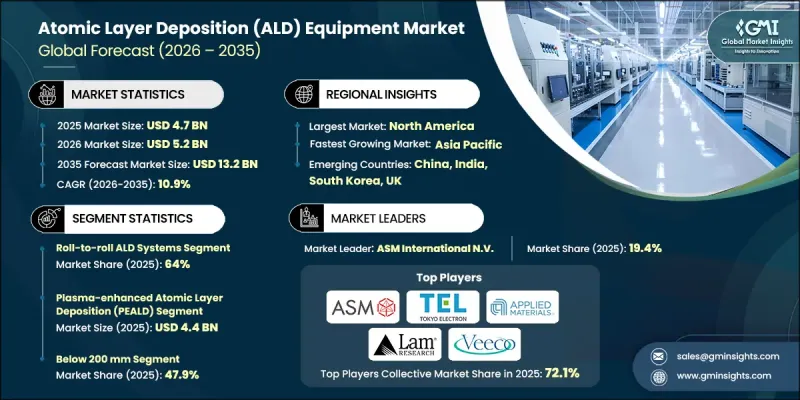
原子層沉積 (ALD) 設備市場的成長主要得益於半導體製造製程的加速發展,在這些製程中,原子級精度對於裝置的性能和可靠性至關重要。新一代記憶體架構的擴展以及對高效能功率電子元件日益成長的需求,都顯著推動了市場需求。此外,ALD 技術在奈米裝置製造和先進封裝解決方案中的應用日益廣泛,也促進了產業成長。半導體製造設施投資的不斷增加,以及對高性能材料的需求,進一步提升了 ALD 系統的重要性。此外,需要在複雜結構上實現均勻薄膜沉積的創新製造技術的應用,也在推動市場發展,支持現代電子產品的演進,並確保產業的長期持續成長。
| 市場範圍 | |
|---|---|
| 開始年份 | 2025 |
| 預測期 | 2026-2035 |
| 上市時的市場規模 | 47億美元 |
| 預測金額 | 132億美元 |
| 複合年成長率 | 10.9% |
原子層沉積 (ALD) 設備市場持續成長,主要受先進半導體製造製程需求不斷成長的推動。隨著製造商朝向更精細、更複雜的製程節點邁進,對材料沉積的精確控制變得日益重要。寬能隙半導體材料的日益普及進一步加速了對高品質沉積系統的需求。這些材料需要可靠的薄膜塗層,以確保在高功率、高頻應用中發揮最佳性能。此外,ALD 技術在先進封裝和微型元件製造領域的作用日益增強,也推動其在多個終端應用產業的應用。製造技術的持續創新和半導體製造基礎設施資本投入的增加,進一步鞏固了市場前景。
受市場對高度可控和靈活沉積製程需求的不斷成長的推動,預計到2035年,單晶圓原子層沉積(ALD)系統市場將以10.2%的複合年成長率成長。這些系統能夠精確控制薄膜厚度並適應複雜的裝置結構,是下一代半導體製造的理想選擇。它們能夠容納多層材料和先進的晶片設計,持續推動高效能運算和儲存應用領域的採用。該市場受益於製造製程客製化和高精度需求的不斷成長,從而鞏固了其在不斷發展的半導體行業中的地位。
預計2025年,等離子體增強原子層沉積(PEALD)市場規模將達到44億美元。其強大的市場地位歸功於其能夠在相對較低的溫度下沉積高品質薄膜,使其適用於光敏基基板和先進裝置結構。該技術有助於改善薄膜性能、提高均勻性並增強與複雜半導體架構的整合。其對先進製造需求的適用性確保了高階製造環境中的持續需求,使其成為更廣泛的原子層沉積設備市場中的關鍵組成部分。
預計到2025年,北美原子層沉積(ADD)設備市佔率將達到36.5%,這主要得益於半導體製造和先進材料研究領域投資的不斷成長。該地區對高效能運算技術日益成長的需求正在加速精密ADD設備的應用。不斷擴大的製造能力和持續的技術進步也為該地區的成長提供了支撐。此外,對創新和下一代半導體解決方案開發的重視也進一步促進了市場擴張。預計在整個預測期內,對製造設施和材料工程的持續投資將使該地區保持競爭優勢。
目錄
第1章:調查方法和範圍
第2章執行摘要
第3章業界考察
- 生態系分析
- 供應商情況
- 利潤率
- 成本結構
- 每個階段增加的價值
- 影響價值鏈的因素
- 中斷
- 影響產業的因素
- 促進因素
- 對先進半導體節點製造的需求不斷成長
- 電力電子和寬能隙半導體的發展
- 晶片中高介電常數材料的應用日益廣泛
- 擴大3D NAND和DRAM記憶體生產
- 複雜半導體結構中對三防膠的需求
- 產業潛在風險與挑戰
- ALD元件系統的高額資本投資成本
- 與其他技術相比,薄膜沉積速率較慢。
- 市場機遇
- 先進封裝技術中ALD技術的應用日益廣泛
- 在微機電系統和奈米裝置領域的應用不斷擴展
- 促進因素
- 成長潛力分析
- 監理情勢
- 北美洲
- 歐洲
- 亞太地區
- 拉丁美洲
- 中東和非洲
- 波特五力分析
- PESTEL 分析
- 科技與創新趨勢
- 當前技術趨勢
- 新興技術
- 價格趨勢
- 按地區
- 依產品
- 定價策略
- 新興經營模式
- 合規要求
- 專利和智慧財產權分析
第4章 競爭情勢
- 介紹
- 企業市佔率分析
- 按地區
- 北美洲
- 歐洲
- 亞太地區
- 拉丁美洲
- 中東和非洲
- 市場集中度分析
- 按地區
- 主要企業的競爭標竿分析
- 財務績效比較
- 銷售量
- 利潤率
- 研究與開發
- 產品系列比較
- 產品線寬度
- 科技
- 創新
- 區域擴張比較
- 全球擴張分析
- 服務網路覆蓋
- 按地區分類的市場滲透率
- 競爭定位矩陣
- 領導者
- 挑戰者
- 追蹤者
- 小眾玩家
- 戰略展望矩陣
- 財務績效比較
- 主要進展
- 併購
- 夥伴關係與合作
- 技術進步
- 擴張和投資策略
- 數位轉型計劃
- 新興競爭對手和Start-Ups競爭對手的發展趨勢
第5章 市場估算與預測:依設備類型分類,2022-2035年
- 單晶圓ALD系統
- 批量ALD系統
- 空間ALD系統
- 卷對卷ALD系統
第6章 市場估計與預測:依技術類型分類,2022-2035年
- 熱原子層沉積
- 等離子體增強原子層沉積(PEALD)
第7章 依晶圓尺寸分類的市場估算與預測,2022-2035年
- 300 mm
- 200 mm
- 小於200毫米
第8章 市場估計與預測:依應用領域分類,2022-2035年
- 邏輯儲存設備
- 微機電系統和感測器
- 電力電子
- 光電子學
- 儲能
第9章 市場估計與預測:依最終用戶產業分類,2022-2035年
- 半導體製造商
- 電子和光電子設備製造商
- 能源和電池製造商
- 研究機構
- 其他
第10章 市場估價與預測:依地區分類,2022-2035年
- 北美洲
- 美國
- 加拿大
- 歐洲
- 德國
- 英國
- 法國
- 西班牙
- 義大利
- 荷蘭
- 亞太地區
- 中國
- 印度
- 日本
- 澳洲
- 韓國
- 拉丁美洲
- 巴西
- 墨西哥
- 阿根廷
- 中東和非洲
- 南非
- 沙烏地阿拉伯
- 阿拉伯聯合大公國
第11章:公司簡介
- 主要企業
- Applied Materials, Inc.
- ASM International NV
- Lam Research Corporation
- Tokyo Electron Limited
- Veeco Instruments Inc.
- 按地區分類的主要企業
- 北美洲
- Arradiance, LLC
- CVD Equipment Corporation
- Kurt J. Lesker Company
- Nano-Master, Inc.
- SVT Associates
- 亞太地區
- Hitachi High-Technologies Corporation
- SHOWA SHINKU CO., LTD.
- Watty Corporation
- 歐洲
- Aixtron SE
- Beneq Oy
- Oxford Instruments plc
- SENTECH Instruments GmbH
- Meyer Burger
- 北美洲
- 特殊玩家/干擾者
- ANRIC Technologies
- Cambridge NanoTech
- Entegris Inc.
- Forge Nano Inc.
- MSE Supplies LLC
- Picosun Oy
- Radiation Monitoring Devices, Inc.
The Global Atomic Layer Deposition Equipment Market was valued at USD 4.7 billion in 2025 and is estimated to grow at a CAGR of 10.9% to reach USD 13.2 billion by 2035.
Growth across the atomic layer deposition equipment market is being driven by the accelerating shift toward advanced semiconductor manufacturing nodes, where precision at the atomic level is essential for device performance and reliability. The expansion of next-generation memory architectures and the growing demand for high-efficiency power electronics are significantly contributing to market demand. In addition, increasing integration of ALD technologies in nanoscale device fabrication and advanced packaging solutions is strengthening industry growth. Rising investments in semiconductor fabrication facilities, coupled with the need for high-performance materials, are reinforcing the importance of ALD systems. The market is also benefiting from the adoption of innovative manufacturing techniques that require consistent thin-film deposition across complex structures, supporting the evolution of modern electronics and ensuring long-term industry expansion.
| Market Scope | |
|---|---|
| Start Year | 2025 |
| Forecast Year | 2026-2035 |
| Start Value | $4.7 Billion |
| Forecast Value | $13.2 Billion |
| CAGR | 10.9% |
The atomic layer deposition equipment market continues to gain traction from the rising demand for advanced semiconductor fabrication processes. As manufacturers move toward smaller and more complex nodes, precise control over material deposition becomes increasingly critical. The growing adoption of wide-bandgap semiconductor materials is further accelerating demand for high-quality deposition systems. These materials require reliable thin-film coatings to ensure optimal performance in high-power and high-frequency applications. Additionally, the increasing role of ALD technology in advanced packaging and micro-scale device production is enhancing its adoption across multiple end-use industries. Continuous innovation in fabrication technologies and increased capital spending on semiconductor manufacturing infrastructure are further strengthening the market outlook.
The single-wafer ALD systems segment is expected to grow at a CAGR of 10.2% through 2035, supported by rising demand for highly controlled and flexible deposition processes. These systems offer precise film thickness control and adaptability for complex device architectures, making them highly suitable for next-generation semiconductor manufacturing. Their ability to support multiple material layers and advanced chip designs continues to drive adoption across high-performance computing and memory applications. The segment benefits from increasing requirements for customization and precision in fabrication processes, reinforcing its role in the evolving semiconductor landscape.
The plasma-enhanced atomic layer deposition segment reached USD 4.4 billion in 2025. Its strong market presence is attributed to its capability to deposit high-quality thin films at comparatively lower temperatures, making it suitable for sensitive substrates and advanced device structures. The technology supports improved film properties, enhanced uniformity, and better integration with complex semiconductor architectures. Its compatibility with advanced manufacturing requirements continues to sustain demand across high-end fabrication environments, positioning it as a critical component within the broader atomic layer deposition equipment market.
North America Atomic Layer Deposition Equipment Market accounted for 36.5% share in 2025, driven by increasing investments in semiconductor manufacturing and advanced materials research. The region is witnessing growing demand for high-performance computing technologies, which is accelerating the adoption of precision deposition equipment. Expanding manufacturing capabilities and continuous technological advancements are supporting regional growth. In addition, a strong focus on innovation and development of next-generation semiconductor solutions is further contributing to the expansion of the market. Ongoing investments in fabrication facilities and materials engineering are expected to maintain the region's competitive position over the forecast period.
Key players in the Global Atomic Layer Deposition Equipment Market Aixtron SE, ANRIC Technologies, Applied Materials Inc., Arradiance LLC, ASM International NV, Beneq Oy, Cambridge NanoTech, CVD Equipment Corporation, Entegris Inc., Forge Nano Inc., Hitachi High-Technologies Corporation, Kurt J. Lesker Company, Lam Research Corporation, Meyer Burger, MSE Supplies LLC, Nano-Master Inc., Oxford Instruments plc, Picosun Oy, Radiation Monitoring Devices Inc., SENTECH Instruments GmbH, SHOWA SHINKU CO. LTD., SVT Associates, Tokyo Electron Limited, Veeco Instruments Inc., Watty Corporation. Companies operating in the atomic layer deposition equipment market are focusing on strengthening their market position through continuous technological innovation, strategic collaborations, and expansion of production capabilities. They are investing heavily in research and development to enhance deposition precision, improve throughput, and develop advanced materials compatible with next-generation semiconductor nodes. Partnerships with semiconductor manufacturers and research institutions are enabling companies to co-develop tailored solutions that meet evolving industry requirements. Firms are also expanding their global footprint by establishing new manufacturing facilities and strengthening supply chain networks to ensure consistent product availability. Additionally, companies are prioritizing product differentiation through improved efficiency, reduced operational costs, and enhanced system integration capabilities.
Table of Contents
Chapter 1 Methodology and Scope
- 1.1 Market scope and definition
- 1.2 Research design
- 1.2.1 Research approach
- 1.2.2 Data collection methods
- 1.3 Data mining sources
- 1.3.1 Global
- 1.3.2 Regional/Country
- 1.4 Base estimates and calculations
- 1.4.1 Base year calculation
- 1.4.2 Key trends for market estimation
- 1.5 Primary research and validation
- 1.5.1 Primary sources
- 1.6 Forecast model
- 1.7 Research assumptions and limitations
Chapter 2 Executive Summary
- 2.1 Industry 360° synopsis, 2022 - 2035
- 2.2 Key market trends
- 2.2.1 Equipment type trends
- 2.2.2 Technology type trends
- 2.2.3 Wafer size trends
- 2.2.4 Application trends
- 2.2.5 End-user industry trends
- 2.2.6 Regional trends
- 2.3 TAM Analysis, 2026-2035
- 2.4 CXO perspectives: Strategic imperatives
Chapter 3 Industry Insights
- 3.1 Industry ecosystem analysis
- 3.1.1 Supplier Landscape
- 3.1.2 Profit Margin
- 3.1.3 Cost structure
- 3.1.4 Value addition at each stage
- 3.1.5 Factor affecting the value chain
- 3.1.6 Disruptions
- 3.2 Industry impact forces
- 3.2.1 Growth drivers
- 3.2.1.1 Rising demand for advanced semiconductor node fabrication
- 3.2.1.2 Growth in power electronics and wide-bandgap semiconductors
- 3.2.1.3 Growing adoption of high-k dielectric materials in chips
- 3.2.1.4 Expansion of 3D NAND and DRAM memory production
- 3.2.1.5 Demand for conformal coatings in complex semiconductor structures
- 3.2.2 Industry pitfalls and challenges
- 3.2.2.1 High capital cost of ALD equipment systems
- 3.2.2.2 Slow deposition rates compared to alternative techniques
- 3.2.3 Market opportunities
- 3.2.3.1 Increasing ALD adoption in advanced packaging technologies
- 3.2.3.2 Growing applications in MEMS and nanoscale devices
- 3.2.1 Growth drivers
- 3.3 Growth potential analysis
- 3.4 Regulatory landscape
- 3.4.1 North America
- 3.4.2 Europe
- 3.4.3 Asia Pacific
- 3.4.4 Latin America
- 3.4.5 Middle East & Africa
- 3.5 Porter's analysis
- 3.6 PESTEL analysis
- 3.7 Technology and Innovation landscape
- 3.7.1 Current technological trends
- 3.7.2 Emerging technologies
- 3.8 Price trends
- 3.8.1 By region
- 3.8.2 By product
- 3.9 Pricing Strategies
- 3.10 Emerging Business Models
- 3.11 Compliance Requirements
- 3.12 Patent and IP analysis
Chapter 4 Competitive Landscape, 2025
- 4.1 Introduction
- 4.2 Company market share analysis
- 4.2.1 By region
- 4.2.1.1 North America
- 4.2.1.2 Europe
- 4.2.1.3 Asia Pacific
- 4.2.1.4 Latin America
- 4.2.1.5 Middle East & Africa
- 4.2.2 Market concentration analysis
- 4.2.1 By region
- 4.3 Competitive benchmarking of key players
- 4.3.1 Financial performance comparison
- 4.3.1.1 Revenue
- 4.3.1.2 Profit margin
- 4.3.1.3 R&D
- 4.3.2 Product portfolio comparison
- 4.3.2.1 Product range breadth
- 4.3.2.2 Technology
- 4.3.2.3 Innovation
- 4.3.3 Geographic presence comparison
- 4.3.3.1 Global footprint analysis
- 4.3.3.2 Service network coverage
- 4.3.3.3 Market penetration by region
- 4.3.4 Competitive positioning matrix
- 4.3.4.1 Leaders
- 4.3.4.2 Challengers
- 4.3.4.3 Followers
- 4.3.4.4 Niche players
- 4.3.5 Strategic outlook matrix
- 4.3.1 Financial performance comparison
- 4.4 Key developments
- 4.4.1 Mergers and acquisitions
- 4.4.2 Partnerships and collaborations
- 4.4.3 Technological advancements
- 4.4.4 Expansion and investment strategies
- 4.4.5 Digital transformation initiatives
- 4.5 Emerging/ startup competitors landscape
Chapter 5 Market Estimates and Forecast, By Equipment Type, 2022 - 2035 (USD Million)
- 5.1 Key trends
- 5.2 Single-wafer ALD systems
- 5.3 Batch ALD systems
- 5.4 Spatial ALD systems
- 5.5 Roll-to-roll ALD systems
Chapter 6 Market Estimates and Forecast, By Technology Type, 2022 - 2035 (USD Million)
- 6.1 Key trends
- 6.2 Thermal ALD
- 6.3 Plasma-enhanced ALD (PEALD)
Chapter 7 Market Estimates and Forecast, By Wafer Size, 2022 - 2035 (USD Million)
- 7.1 Key trends
- 7.2 300 mm
- 7.3 200 mm
- 7.4 Below 200 mm
Chapter 8 Market Estimates and Forecast, By Application, 2022 - 2035 (USD Million)
- 8.1 Key trends
- 8.2 Logic & memory devices
- 8.3 MEMS & sensors
- 8.4 Power electronics
- 8.5 Optoelectronics
- 8.6 Energy storage
Chapter 9 Market Estimates and Forecast, By End-User Industry, 2022 - 2035 (USD Million)
- 9.1 Key trends
- 9.2 Semiconductor manufacturers
- 9.3 Electronics & optoelectronics manufacturers
- 9.4 Energy & battery manufacturers
- 9.5 Research institutions
- 9.6 Others
Chapter 10 Market Estimates and Forecast, By Region, 2022 - 2035 (USD Million)
- 10.1 Key trends
- 10.2 North America
- 10.2.1 U.S.
- 10.2.2 Canada
- 10.3 Europe
- 10.3.1 Germany
- 10.3.2 UK
- 10.3.3 France
- 10.3.4 Spain
- 10.3.5 Italy
- 10.3.6 Netherlands
- 10.4 Asia Pacific
- 10.4.1 China
- 10.4.2 India
- 10.4.3 Japan
- 10.4.4 Australia
- 10.4.5 South Korea
- 10.5 Latin America
- 10.5.1 Brazil
- 10.5.2 Mexico
- 10.5.3 Argentina
- 10.6 Middle East and Africa
- 10.6.1 South Africa
- 10.6.2 Saudi Arabia
- 10.6.3 UAE
Chapter 11 Company Profiles
- 11.1 Global Key Players
- 11.1.1 Applied Materials, Inc.
- 11.1.2 ASM International NV
- 11.1.3 Lam Research Corporation
- 11.1.4 Tokyo Electron Limited
- 11.1.5 Veeco Instruments Inc.
- 11.2 Regional key players
- 11.2.1 North America
- 11.2.1.1 Arradiance, LLC
- 11.2.1.2 CVD Equipment Corporation
- 11.2.1.3 Kurt J. Lesker Company
- 11.2.1.4 Nano-Master, Inc.
- 11.2.1.5 SVT Associates
- 11.2.2 Asia Pacific
- 11.2.2.1 Hitachi High-Technologies Corporation
- 11.2.2.2 SHOWA SHINKU CO., LTD.
- 11.2.2.3 Watty Corporation
- 11.2.3 Europe
- 11.2.3.1 Aixtron SE
- 11.2.3.2 Beneq Oy
- 11.2.3.3 Oxford Instruments plc
- 11.2.3.4 SENTECH Instruments GmbH
- 11.2.3.5 Meyer Burger
- 11.2.1 North America
- 11.3 Niche Players/Disruptors
- 11.3.1 ANRIC Technologies
- 11.3.2 Cambridge NanoTech
- 11.3.3 Entegris Inc.
- 11.3.4 Forge Nano Inc.
- 11.3.5 MSE Supplies LLC
- 11.3.6 Picosun Oy
- 11.3.7 Radiation Monitoring Devices, Inc.
 原子層沉積(ALD)市場:2026-2032年全球市場預測(依沉積製程、設備類型、塗裝類型、薄膜厚度、基板類型、應用和最終用戶產業分類)
 原子層沉積(ALD)市場:按產品、應用和地區分類原子層沉積設備市場:依設備類型、技術類型、應用和最終用戶產業分類-2026-2032年全球市場預測
 原子層沉積設備市場規模、佔有率、趨勢和預測:按產品、應用和地區分類,2026-2034年全球高階ALD設備市場(按設備類型、技術類型、晶圓尺寸、應用和最終用戶產業分類)預測(2026-2032年)
 全球原子層沉積元件市場規模、佔有率、趨勢和成長分析報告(2026-2034年)原子層沉積(ALD)全球市場規模、佔有率、趨勢和成長分析報告,2026-2034年
 2026年全球原子層沉積市場報告2026年全球ALD設備市場報告
 2026-2030年全球原子層沉積(ALD)市場