


 |
市場調查報告書
商品編碼
2113965
混合光子積體電路:市場佔有率分析、產業趨勢與統計及成長預測(2026-2031)Hybrid Photonic Integrated Circuit - Market Share Analysis, Industry Trends & Statistics, Growth Forecasts (2026 - 2031) |
||||||

※ 本網頁內容可能與最新版本有所差異。詳細情況請與我們聯繫。
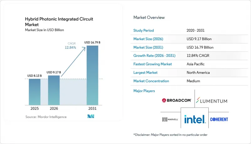
根據 Mordor Intelligence 預測,混合光積體電路的市場規模預計將從 2025 年的 81.3 億美元成長到 2026 年的 91.7 億美元,然後從 2026 年到 2031 年以 12.84% 的複合年成長率成長,到 2031 年達到 167.7.7.00 億美元。
本報告按應用領域(資料通訊及雲端互聯、電信傳輸及5G/6G行動回程等)、材料平台(矽-III-V族混合材料、氮化矽-III-V族材料等)、終端用戶產業(雲端服務供應商、電信業者及網路OEM廠商等)及地區進行細分。市場預測以美元計價。
全球混合光子積體電路市場趨勢與洞察
對人工智慧/機器學習最佳化型共封裝光學元件的需求
目前,訓練一個擁有1兆個參數的模型,其每機架每秒的流量將超過400Terabit。對於前面板插件式設計而言,如果不造成不可接受的功率損耗,就無法達到如此閾值。共封裝光元件透過將光子晶片放置在交換器ASIC旁邊,縮短了電氣傳輸距離,並將跳頻延遲降低到10奈秒以下。 Meta在2024年Grand Teton叢集上展示了其量產準備情況,而Ayar Labs已出貨超過1萬個光晶片,確保了2025年大規模量產的實現。歐洲和印度的「主權人工智慧」法規要求進行本地推理,這推動了對緊湊型光I/O的中等規模部署。早期採用者報告稱,與分離式光元件相比,互連功耗降低了30%,投資回收期縮短了2年,這加速了混合光積體電路市場的普及。
超大規模資料中心頻寬的爆炸性成長
在影片串流媒體和生成式人工智慧的推動下,預計到2026年,全球IP流量將達到4.8澤字節。超大規模資料中心業者預計將在2025年過渡到800Gigabit乙太網路骨幹網,並在2026年過渡到1.6Terabit光纖通訊,從而將更新周期從五年縮短至三年。微軟在2024年將其骨幹網路的60%升級到400Gigabit連貫通訊,使每位元成本降低了35%。隨著速度的提升,鏈路預算變得更加緊張,單片光電協同設計變得更具優勢,從而推動了混合光積體電路市場的需求。薄膜鈮酸鋰的效率比磷化銦高3分貝,可實現低電壓1.6Terabit模組。
異質鍵結中的產量挑戰
將 III-V 族晶片鍵合到 300 毫米矽晶圓上時,良率維持在 92-95%,良率每下降 1 個百分點,單位成本就會增加 3-5%。 Tower Semiconductor 在 2024 年第四季將其良率提高到 94%,但仍未達到汽車級晶片 98% 的目標。熱退火過程中形成的空洞會導致高達 2 分貝的光學損耗,並加速分層。 Imec 的等離子體活化鍵合技術可將空洞減少 70%,但會使製程成本增加 15%。目前獲得認證的代工廠數量有限(僅 5 家),這造成了短期供應瓶頸,在新的產能建立之前,這將限制混合光子積體電路市場的擴張。
細分市場分析
高效能運算 (HPC) 和人工智慧 (AI) 加速器以 13.98% 的複合年成長率 (CAGR) 領先市場,這反映出 GPU 間頻寬的激增已超越電力 SerDes。資料通訊和雲端互連仍佔據最大佔有率,達 46.05%,這主要得益於現有 100 Gigabit和 400 Gigabit鏈路部署向 800 Gigabit光纖通訊的轉變。在各國政府主導的AI 基礎設施建設的推動下,用於 AI 加速器的混合光子積體電路市場預計將在 2026 年至 2031 年間成長至超過 24.5 億美元。通訊回程傳輸、雷射雷達感測和射頻光電由於其特定的性能要求,仍保持小眾但盈利的地位。
從集中式訓練叢集到邊緣推理的轉變正在推動光I/O在伺服器、智慧網卡乃至嵌入式系統中的廣泛應用。 Meta的共封裝解決方案已將機架內延遲降低至10奈秒以下。汽車雷射雷達正朝著1550奈米FMCW設計方向發展,該設計將可調式雷射和連貫接收器整合在單一晶片上,進一步推動了混合方法的應用。射頻光電透過支援下一代雷達所需的40吉赫瞬時頻寬,滿足了國防需求。在醫療診斷領域,利用晶片實驗室光電進行即時病原體檢測的早期臨床試驗正在進行中。
區域分析
北美地區在英特爾新墨西哥州晶圓廠和Ayar Labs大規模量產的支持下,預計2025年將佔全球銷售額的38.10%。根據聯邦《晶片技術創新與應用法案》(CHIPS Act),總計15億美元的津貼正用於光電研究和開發,鞏固了該地區的主導地位。美國雲端服務供應商正在加速部署Gigabit主幹網路,從而推動了對國內晶圓廠的巨大需求。加拿大的量子光電計畫也促進了氮化矽波導管客製化訂單的成長。
亞太地區以13.55%的複合年成長率領跑,主要得益於中國100億美元的晶圓代工扶持計畫及台灣先進的封裝產業叢集。台積電位於松江的試驗線計畫投產混合晶片,目標在2026年達到月產1萬片晶圓。在日本2億美元的光電聯盟中,富士通和NTT正在合作開發1.6Terabit的連貫系統;印度的「半導體計畫」已撥款5億美元用於扶持國內晶圓廠。東南亞的電子製造服務(EMS)供應商正專注於消費光學領域的聚合物光電,從而拓展區域供應鏈。
歐洲受益於imec的多專案晶圓計畫和荷蘭的光刻生態系統,但其混合光積體電路市場規模落後於北美和亞太地區。歐洲的《晶片法案》已撥款5億歐元用於專注於異質鍵合和量子裝置的試點生產線。德國和法國在汽車雷射雷達主導投入巨資,而英國則支持用於生物感測的矽光電。中東電信業者,例如STC,正在為Metrolink部署Gigabit連貫系統,但本地製造規模仍然很小。南非的一個早期非洲先導計畫正在探索矽光電在寬頻存取方面的應用,為未來的普及奠定基礎。
其他好處:
- Excel格式的市場預測(ME)表
- 3個月的分析師支持
目錄
第1章:引言
- 研究假設和市場定義
- 調查範圍
第2章:調查方法
第3章執行摘要
第4章 市場狀況
- 市場概覽
- 市場促進因素
- 對人工智慧/機器學習最佳化的共封裝光學元件的需求
- 超大規模資料中心頻寬的爆炸性成長
- 在 5G/6G去程傳輸和中傳中實現高密度光纖網路覆蓋。
- 矽與III-V族材料異質整合的成本交叉
- 國防雷射雷達和射頻光電採購激增(預算保密)
- 採用新的晶片封裝標準(UCIe-P)
- 市場限制因素
- 與非均勻鍵結產率相關的挑戰
- 由於熱失配導致的可靠性問題
- 混合設計自動化生態系統有其限制。
- 進入資本密集型代工廠的瓶頸(認證生產線少於 5 條)
- 價值鏈分析
- 監理情勢
- 技術展望
- 波特五力分析
第5章 市場規模與成長預測
- 透過使用
- 資料通訊和雲端互連
- 通訊傳輸和 5G/6G行動回程
- LiDAR與光學感測
- 高效能運算 (HPC) 和人工智慧加速器
- 射頻光電和微波光電
- 材料生產
- 矽-III-V族混合材料(矽基InP/GaAs)
- 氮化矽-III-V
- 聚合物光電混合
- 矽基鈮酸鋰薄膜
- 其他(SiGe、AlN 等)
- 按最終用戶行業分類
- 雲端服務供應商(超大規模資料中心業者)
- 電信業者及網路OEM廠商
- 國防/航太
- 醫療保健和生物感測領域的OEM製造商
- 工業和汽車OEM
- 按地區
- 北美洲
- 美國
- 加拿大
- 墨西哥
- 歐洲
- 德國
- 英國
- 法國
- 荷蘭
- 其他歐洲國家
- 亞太地區
- 中國
- 印度
- 日本
- 韓國
- ASEAN
- 其他亞太國家
- 世界其他地區
- 北美洲
第6章 競爭情勢
- 市場集中度
- 策略趨勢
- 市佔率分析
- 公司簡介
- Intel Corporation
- Cisco Systems(Acacia Communications)
- Broadcom Inc.
- Marvell Technology(Inphi)
- Lumentum Holdings
- Coherent Corp.(II-VI)
- Rockley Photonics
- Ayar Labs
- Nokia(Bell Labs)
- Fujitsu Optical Components
- NeoPhotonics(Lumentum)
- Ciena Corporation
- Effect Photonics
- POET Technologies
- Ligentec SA
- Infinera Corporation
- Hewlett Packard Enterprise(HPC interconnect)
- GlobalFoundries(SiPh services)
- Imec(foundry and MPW)
- Tower Semiconductor
第7章 市場機會與未來展望
According to Mordor Intelligence, the hybrid photonic integrated circuit market size is expected to grow from USD 8.13 billion in 2025 to USD 9.17 billion in 2026 and is forecast to reach USD 16.79 billion by 2031 at 12.84% CAGR over 2026-2031.
This report is Segmented by Application (Datacom and Cloud Interconnect, Telecom Transport and 5G/6G Mobile Backhaul, and More), Material Platform (Silicon-III-V Hybrid, Silicon Nitride-III-V, and More), End-User Industry (Cloud Service Providers, Telecom Operators and Network OEMs, and More), and Geography. The Market Forecasts are Provided in Terms of Value (USD).
Global Hybrid Photonic Integrated Circuit Market Trends and Insights
AI/ML-Optimised Co-Packaged Optics Demand
Training trillion-parameter models now drives per-rack traffic beyond 400 terabits per second, a threshold that front-panel pluggables cannot meet without prohibitive power loss. Co-packaged optics place photonic dies beside switch ASICs, trimming electrical reach and delivering sub-10-nanosecond hop latency. Meta validated production readiness in its 2024 Grand Teton cluster, while Ayar Labs shipped more than 10,000 optical chiplets and secured 2025 volume ramps. Sovereign-AI rules in Europe and India require local inference, driving mid-scale deployments that necessitate compact optical I/O. Early adopters report a 30% lower interconnect power and a 2-year payback period versus discrete optics, thereby accelerating the adoption curve of the hybrid photonic integrated circuit market.
Hyperscale Datacenter Bandwidth Explosion
Global IP traffic is projected to reach 4.8 zettabytes in 2026, driven by video streaming and the adoption of generative AI. Hyperscalers are expected to transition to 800 gigabit Ethernet spines in 2025 and 1.6 terabit optics in 2026, thereby compressing refresh cycles from 5 years to 3 years. Microsoft upgraded 60% of its backbone to 400 gigabit coherent in 2024, cutting cost per bit by 35%. Each speed jump tightens the link budget and favors monolithic photonic-electronic co-design, thereby boosting demand for the hybrid photonic integrated circuit market. Thin-film lithium niobate offers 3 decibels higher efficiency than indium phosphide, enabling lower-voltage 1.6 terabit modules.
Heterogeneous Bonding Yield Challenges
Bonding III-V dies on 300 millimeter silicon still reaches only 92 to 95% yield, pushing up unit cost by 3-5% per lost point. Tower Semiconductor improved to 94% in Q4 2024 but remains shy of the 98% goal for automotive grade. Void formation during thermal anneal adds up to 2 decibel optical loss and accelerates delamination. Imec's plasma-activated bonding lowers voids by 70% yet raises process cost by 15%. The limited pool of five qualified foundries acts as a near-term supply cap and restrains the hybrid photonic integrated circuit market until new capacity matures.
Other drivers and restraints analyzed in the detailed report include:
- 5G/6G Fronthaul and Mid-Haul Optical Densification
- Silicon + III-V Heterointegration Cost Crossover
- Thermal Mismatch Reliability Issues
For complete list of drivers and restraints, kindly check the Table Of Contents.
Segment Analysis
High-Performance Computing and AI Accelerators account for the fastest 13.98% CAGR, reflecting surging inter-GPU bandwidth that outstrips electrical SerDes. Datacom and Cloud Interconnect remains the largest slice with 46.05%, supported by the installed base of 100 and 400 gigabit links that migrate to 800 gigabit optics. The hybrid photonic integrated circuit market size for AI accelerators is projected to add more than USD 2.45 billion between 2026 and 2031, driven by sovereign-AI buildouts in Europe and Asia. Telecom backhaul, LiDAR sensing, and RF-photonics retain niche but profitable positions thanks to specialized performance needs.
The shift from centralized training clusters to edge inference pushes optical I/O into servers, smart NICs, and even embedded systems. Meta's co-packaged deployment cut intra-rack latency under 10 nanoseconds. Automotive LiDAR is moving to 1550-nanometer FMCW designs that integrate tunable lasers and coherent receivers on a single die, reinforcing hybrid adoption. RF-photonics supports a 40-gigahertz instantaneous bandwidth for next-generation radar, meeting defense demand. Healthcare diagnostics enter early trials with lab-on-chip photonics for real-time pathogen detection.
Complete Report Scope:
- By Application
- Datacom and Cloud Interconnect
- Telecom Transport and 5G/6G Mobile Backhaul
- LiDAR and Optical Sensing
- High-performance Computing (HPC) and AI Accelerators
- RF-Photonics and Microwave Photonics
- By Material Platform
- Silicon-III-V Hybrid (InP/GaAs on Si)
- Silicon Nitride-III-V
- Polymer Photonics Hybrid
- Thin-film Lithium Niobate on Si
- Others (SiGe, AlN, etc.)
- By End-user Industry
- Cloud Service Providers (Hyperscalers)
- Telecom Operators and Network OEMs
- Defense and Aerospace
- Healthcare and Biosensing OEMs
- Industrial and Automotive OEMs
- By Geography
- North America
- United States
- Canada
- Mexico
- Europe
- Germany
- United Kingdom
- France
- Netherlands
- Rest of Europe
- Asia-Pacific
- China
- India
- Japan
- South Korea
- ASEAN
- Rest of Asia-Pacific
- Rest of the World
- North America
Geography Analysis
North America held 38.10% of 2025 revenue, buoyed by Intel's New Mexico fab and Ayar Labs volume shipments. The Federal CHIPS Act grants, totaling USD 1.5 billion, earmark photonics R&D, ensuring local leadership. Cloud builders in the United States fast-track 800 gigabit spines, pulling high-volume demand into domestic fabs. Canada's quantum photonics programs add specialty orders for silicon nitride waveguides.
Asia-Pacific posts the highest 13.55% CAGR, driven by China's USD 10 billion foundry stimulus and Taiwan's advanced packaging clusters. TSMC's Songjiang pilot line is set to begin hybrid die runs, targeting 10,000 wafers per month by 2026. Japan's USD 200 million photonics consortium teams Fujitsu and NTT on a 1.6 terabit coherent system, while India's Semiconductor Mission allocates USD 500 million for local fabs. South-East Asian EMS vendors eye polymer photonics for consumer optics, extending regional supply chains.
Europe benefits from Imec's multi-project wafer program and the Netherlands' lithography ecosystem; however, its hybrid photonic integrated circuit market size lags behind that of North America and the Asia-Pacific region. The European Chips Act reserves EUR 500 million for pilot lines focused on heterogeneous bonding and quantum devices. Germany and France direct automotive LiDAR funding, while the U.K. backs silicon photonics for biosensing. Middle East operators like STC install 400 gigabit coherent for metro links, though local manufacturing remains minimal. Africa's early pilots in South Africa explore silicon photonics for broadband access, setting a foundation for future uptake.
- Intel Corporation
- Cisco Systems (Acacia Communications)
- Broadcom Inc.
- Marvell Technology (Inphi)
- Lumentum Holdings
- Coherent Corp. (II-VI)
- Rockley Photonics
- Ayar Labs
- Nokia (Bell Labs)
- Fujitsu Optical Components
- NeoPhotonics (Lumentum)
- Ciena Corporation
- Effect Photonics
- POET Technologies
- Ligentec SA
- Infinera Corporation
- Hewlett Packard Enterprise (HPC interconnect)
- GlobalFoundries (SiPh services)
- Imec (foundry and MPW)
- Tower Semiconductor
Additional Benefits:
- The market estimate (ME) sheet in Excel format
- 3 months of analyst support
TABLE OF CONTENTS
1 INTRODUCTION
- 1.1 Study Assumptions and Market Definition
- 1.2 Scope of the Study
2 RESEARCH METHODOLOGY
3 EXECUTIVE SUMMARY
4 MARKET LANDSCAPE
- 4.1 Market Overview
- 4.2 Market Drivers
- 4.2.1 AI/ML-optimised co-packaged optics demand
- 4.2.2 Hyperscale datacenter bandwidth explosion
- 4.2.3 5G/6G fronthaul and mid-haul optical densification
- 4.2.4 Silicon + III-V heterointegration cost crossover
- 4.2.5 Defense LiDAR and RF-photonics procurement surge (classified budgets)
- 4.2.6 Emerging chiplet packaging standards (UCIe-P) adoption
- 4.3 Market Restraints
- 4.3.1 Heterogeneous bonding yield challenges
- 4.3.2 Thermal mismatch reliability issues
- 4.3.3 Limited ecosystem for hybrid design automation
- 4.3.4 Capital-intensive foundry access bottleneck (less than 5 qualified lines)
- 4.4 Value Chain Analysis
- 4.5 Regulatory Landscape
- 4.6 Technological Outlook
- 4.7 Porter's Five Forces Analysis
- 4.7.1 Threat of New Entrants
- 4.7.2 Bargaining Power of Suppliers
- 4.7.3 Bargaining Power of Buyers
- 4.7.4 Threat of Substitutes
- 4.7.5 Competitive Rivalry
5 MARKET SIZE AND GROWTH FORECASTS (VALUE)
- 5.1 By Application
- 5.1.1 Datacom and Cloud Interconnect
- 5.1.2 Telecom Transport and 5G/6G Mobile Backhaul
- 5.1.3 LiDAR and Optical Sensing
- 5.1.4 High-performance Computing (HPC) and AI Accelerators
- 5.1.5 RF-Photonics and Microwave Photonics
- 5.2 By Material Platform
- 5.2.1 Silicon-III-V Hybrid (InP/GaAs on Si)
- 5.2.2 Silicon Nitride-III-V
- 5.2.3 Polymer Photonics Hybrid
- 5.2.4 Thin-film Lithium Niobate on Si
- 5.2.5 Others (SiGe, AlN, etc.)
- 5.3 By End-user Industry
- 5.3.1 Cloud Service Providers (Hyperscalers)
- 5.3.2 Telecom Operators and Network OEMs
- 5.3.3 Defense and Aerospace
- 5.3.4 Healthcare and Biosensing OEMs
- 5.3.5 Industrial and Automotive OEMs
- 5.4 By Geography
- 5.4.1 North America
- 5.4.1.1 United States
- 5.4.1.2 Canada
- 5.4.1.3 Mexico
- 5.4.2 Europe
- 5.4.2.1 Germany
- 5.4.2.2 United Kingdom
- 5.4.2.3 France
- 5.4.2.4 Netherlands
- 5.4.2.5 Rest of Europe
- 5.4.3 Asia-Pacific
- 5.4.3.1 China
- 5.4.3.2 India
- 5.4.3.3 Japan
- 5.4.3.4 South Korea
- 5.4.3.5 ASEAN
- 5.4.3.6 Rest of Asia-Pacific
- 5.4.4 Rest of the World
- 5.4.1 North America
6 COMPETITIVE LANDSCAPE
- 6.1 Market Concentration
- 6.2 Strategic Moves
- 6.3 Market Share Analysis
- 6.4 Company Profiles (includes Global level Overview, Market level overview, Core Segments, Financials as available, Strategic Information, Market Rank/Share for key companies, Products and Services, and Recent Developments)
- 6.4.1 Intel Corporation
- 6.4.2 Cisco Systems (Acacia Communications)
- 6.4.3 Broadcom Inc.
- 6.4.4 Marvell Technology (Inphi)
- 6.4.5 Lumentum Holdings
- 6.4.6 Coherent Corp. (II-VI)
- 6.4.7 Rockley Photonics
- 6.4.8 Ayar Labs
- 6.4.9 Nokia (Bell Labs)
- 6.4.10 Fujitsu Optical Components
- 6.4.11 NeoPhotonics (Lumentum)
- 6.4.12 Ciena Corporation
- 6.4.13 Effect Photonics
- 6.4.14 POET Technologies
- 6.4.15 Ligentec SA
- 6.4.16 Infinera Corporation
- 6.4.17 Hewlett Packard Enterprise (HPC interconnect)
- 6.4.18 GlobalFoundries (SiPh services)
- 6.4.19 Imec (foundry and MPW)
- 6.4.20 Tower Semiconductor
7 MARKET OPPORTUNITIES AND FUTURE OUTLOOK
- 7.1 White-space and Unmet-need Assessment

 厚膜晶片電阻器膏市場報告:趨勢、預測及競爭分析(至2035年)
 2026年全球混合光子積體電路市場報告
 光子量子計算市場機會、成長要素、產業趨勢分析及2026-2035年預測
 光子整合運算市場預測至2034年-全球分析(按整合類型、組件、材料平台、運算架構、波長範圍、應用、最終用戶和地區分類)
 全球光計算市場(2026-2036 年)全球量子光學計算市場(2026-2036 年)
 無線電頻率積體電路(RFIC) 市場分析及至 2035 年預測:按類型、產品類型、技術、組件、應用、材料類型、裝置、最終用戶、功能和安裝配置分類
 光子量子電腦市場可印刷光子電路市場分析及預測(至2035年):依類型、產品類型、技術、組件、應用、材料類型、裝置、製程及最終用戶分類2026年全球厚膜混合積體電路市場報告