


 |
市場調查報告書
商品編碼
2113496
3D TSV元件:市場佔有率分析、產業趨勢與統計資料、成長預測(2026-2031年)3D TSV Devices - Market Share Analysis, Industry Trends & Statistics, Growth Forecasts (2026 - 2031) |
||||||

※ 本網頁內容可能與最新版本有所差異。詳細情況請與我們聯繫。
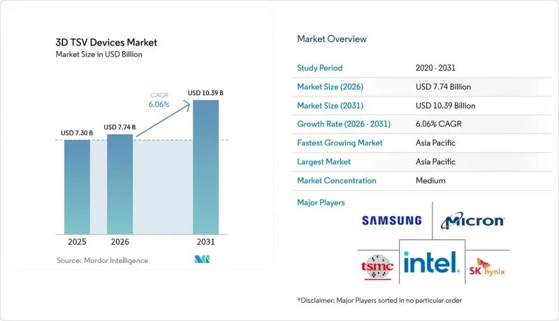
據 Mordor Intelligence 稱,2026 年 3D TSV 裝置的市場規模估計為 77.4 億美元,高於 2025 年的 73 億美元,預計到 2031 年將達到 103.9 億美元。
預計 2026 年至 2031 年的複合年成長率為 6.06%。
本報告按產品類型(成像和光電子、記憶體、其他)、TSV 技術(中間通孔、後通孔、先通孔)、晶圓尺寸(200mm 以下、300mm、450mm)、終端用戶產業(家用電子電器、汽車、IT 和電信、其他)以及地區(北美、南美、歐洲、其他)進行細分。市場預測以美元 (USD) 為單位。
全球3D TSV元件市場趨勢與洞察
對高效能運算和人工智慧工作負載的需求日益成長
大規模語言模型的訓練參數如今已超過1兆個,記憶體層級也被迫超越GDDR6。 SK海力士的12層堆疊式HBM4工程樣品實現了2.1 Tbit/s的頻寬,比HBM3E提升了64%,為GPU叢集提供了足夠的峰值矩陣乘法處理能力。將於2024年核准的JEDEC HBM4標準規定了2048位元介面,而這只能穿透矽通孔(TSV)架構來實現。根據美光2024年的報告,HBM的銷量已成長超過一倍,並已累計15億美元用於2026年的產能擴張。三星轉向銅-銅混合鍵合技術,將通孔電阻降低了40%,並提高了數GHz頻段的訊號完整性。英特爾的 Gaudi 3 加速器在矽中介層上整合了八個 HBM3E 堆疊,這推動了亞利桑那州和新墨西哥州封裝設施 35 億美元的擴建,該項目由 CHIPS 法案共同資助。
資料中心的擴張正在推動高頻寬記憶體的普及。
超大規模資料中心業者正以前所未有的速度部署人工智慧伺服器,NVIDIA H200 和 AMD MI300X 的每個插槽都消耗超過 80GB 的 HBM3 記憶體。台積電的 CoWoS 生產線在 2024 年全年保持 100% 以上的運轉率,促使其在台灣的產能擴張至每月 6 萬片晶圓(投資額達 28 億美元)。根據美光 2024 年 5 月發布的投資者資料,HBM 的供應已排滿至 2025 年,這可能導致平均售價上漲 30%。博通已交付客製化的 AI ASIC,將基於 TSV 的 HBM 整合到每個晶片中,實現了每個封裝超過 3 Tbit/s 的頻寬。這些進展正在增強 3D TSV 裝置市場的短期定價權。
3D TSV封裝單價高
TSV封裝將使每台設備的成本增加15至40美元,從而擠壓中階智慧型手機和物聯網設備的利潤空間。蝕刻設備每個腔室的成本超過1500萬美元,電鍍系統則需額外花費800萬美元。根據安姆科(Amcor)2024年的財務報告,其先進封裝業務的毛利率為28%,比焊線業務低500個基點。認證週期漫長。以日月光(ASE)高雄工廠擴建為例,車規級TSV封裝需要1000小時的高溫運轉測試(HTOL),這可能會使產品上市時間延長至多16週。
細分市場分析
到2025年,儲存裝置將佔3D TSV元件市場45.92%的佔有率,因為HBM已成為人工智慧加速器事實上的高頻寬解決方案。預計到2031年,用於MEMS和感測器的3D TSV元件市場將以8.57%的複合年成長率成長,這反映了汽車雷達和慣性測量設備的應用。成像和光電子產業正受益於後通孔TSV技術,該技術使SONY的背照式感測器在近紅外線區域實現了90%的量子效率。 LED供應商正在採用先通孔TSV技術來驅動microLED顯示器,但由於良率低於60%,大規模應用進展緩慢。
此外,TSV也被應用於電源管理IC和射頻前端等產品中,以最大限度地降低電感。高通的QTM565毫米波模組在1立方厘米的封裝內實現了10 Gb/s的傳輸速率,而博世的BMA580加速計透過堆疊MEMS和ASIC晶片,將待機電流降低至1µA。這些例子表明,即使HBM的獲利能力已達到極限,3D TSV元件產業仍在向記憶體以外的領域擴展。
隨著DRAM和CIS技術的成熟,「中間通孔」預計到2025年將佔銷售額的54.15%,但「優先通孔」技術正以7.69%的複合年成長率成長,因為基於晶片組的晶片需要小於1µm的套刻精度。英特爾的Foveros產品線目前實現了36µm的通孔間距,並計劃在2026年達到10µm,從而實現超過1Tbit/s/mm²的垂直頻寬。
在感測器領域,採用通孔後置法仍然至關重要,它可以維持超過 95% 的像素填充率。三種方法中的混合鍵結技術可使互連密度翻倍,預計將從 2026 年起成為主流,從而鞏固 TSV 作為 3D TSV 裝置市場基石的地位。
區域分析
預計到2025年,亞太地區將佔全球銷售額的42.70%,複合年成長率達8.56%。這主要得益於台積電佔據超過70%的CoWoS產能、三星在HBM市場45%的佔有率,以及SK海力士在利川實現端到端一體化生產。在日本,預計政府將提供9,200億日圓的補貼,用於在2026年前將先進封裝技術引入熊本,為SONY和電裝等公司供貨。中國的長江儲存計畫利用TSV技術堆疊3D NAND快閃記憶體控制器,但出口限制正在減緩其擴張速度。在韓國,一項26兆韓元的稅收優惠將使SK海力士能夠安裝50個新的TSV蝕刻室。印度已獲得美光公司 27.5 億美元的投資,將於 2026 年開始在古吉拉突邦運作OSAT 工廠,將鞏固亞洲作為 3D TSV 裝置市場中心的地位。
到2025年,北美將佔據約34.40%的市場佔有率。美光科技已根據《晶片法案》(CHIPS Act)獲得61.65億美元的資金,用於在紐約州和愛達荷州建造HBM晶片製造工廠。安姆科公司投資20億美元的亞利桑那州工廠計畫於2027年投產,將為汽車和國防工業生產300毫米TSV封裝。英特爾計劃在2026年將其Foveros晶片的產能提高三倍,擴建位於新墨西哥州和亞利桑那州的工廠。同時,加拿大正在渥太華投資2.4億加元建設一條共封裝光學元件(CPO)試點生產線。隨著近岸外包的推進,德克薩斯和恩智浦半導體已將扇出型組裝轉移到墨西哥,但該地區仍缺乏TSV封裝設備。
截至2025年,歐洲市佔率約為18.55%。意法半導體(STMicroelectronics)獲得了29億歐元的資金,用於擴建其位於法國的300毫米TSV生產線。英飛凌(Infineon)在德勒斯登的工廠成功獲得了用於GaN功率元件的通孔中間TSV認證,導通電阻降低了35%。弗勞恩霍夫IZM研究所利用混合鍵合技術,率先實現了0微米間距的裝置生產。英國投資5000萬英鎊建造了一條用於高溫電動車逆變器的GaN TSV生產線。南美洲和中東及非洲(MEA)總合佔4.35%的市場佔有率,但巴西和阿拉伯聯合大公國(UAE)已表示計劃從2027年起提高產能。
其他好處:
- Excel格式的市場預測(ME)表
- 3個月的分析師支持
目錄
第1章:引言
- 研究假設和市場定義
- 調查範圍
第2章:調查方法
第3章執行摘要
第4章 市場狀況
- 市場概覽
- 市場促進因素
- 對高效能運算和人工智慧工作負載的需求日益成長
- 資料中心的擴張正在推動高頻寬記憶體的普及。
- 智慧型手機和家用電子電器的快速小型化
- 基於晶片組的異質整合架構
- 矽光電中3D中介層堆疊的必要性
- 政府對先進包裝工廠的補貼
- 市場限制因素
- 3D TSV封裝單價高
- 熱效應導致可靠性和產量方面的挑戰
- TSV蝕刻和填充設備的供應鏈瓶頸
- 加強對TSV(總特定物項)化學成分的環境法規
- 產業價值鏈分析
- 監理情勢
- 技術展望
- 宏觀經濟因素的影響
- 波特五力分析
第5章 市場規模與成長預測
- 依產品類型
- 成像與光電子學
- 記憶
- 微機電系統/感測器
- LED
- 其他產品
- TSV技術
- Via MiddleTSV
- Via-Last TSV
- Via-FirstTSV
- 按晶圓尺寸
- 200毫米或更小
- 300 mm
- 450 mm
- 按最終用戶行業分類
- 家用電子產品
- 車
- IT/通訊
- 衛生保健
- 航太/國防
- 其他終端用戶產業
- 按地區
- 北美洲
- 美國
- 加拿大
- 墨西哥
- 南美洲
- 巴西
- 阿根廷
- 其他南美國家
- 歐洲
- 德國
- 英國
- 法國
- 義大利
- 西班牙
- 俄羅斯
- 其他歐洲國家
- 亞太地區
- 中國
- 日本
- 印度
- 韓國
- 澳洲
- 其他亞太國家
- 中東和非洲
- 中東
- 沙烏地阿拉伯
- 阿拉伯聯合大公國
- 土耳其
- 其他中東國家
- 非洲
- 南非
- 奈及利亞
- 埃及
- 其他非洲國家
- 中東
- 北美洲
第6章 競爭情勢
- 市場集中度
- 策略趨勢
- 市佔率分析
- 公司簡介
- Taiwan Semiconductor Manufacturing Company Limited
- Samsung Electronics Co., Ltd.
- Intel Corporation
- Micron Technology, Inc.
- SK hynix Inc.
- Toshiba Electronic Devices and Storage Corporation
- ASE Technology Holding Co., Ltd.
- Amkor Technology, Inc.
- United Microelectronics Corporation
- STMicroelectronics NV
- Broadcom Inc.
- Texas Instruments Incorporated
- GlobalFoundries Inc.
- Advanced Micro Devices, Inc.
- Qualcomm Incorporated
- JCET Group Co., Ltd.
- Powertech Technology Inc.
- Siliconware Precision Industries Co., Ltd.
- Xilinx, Inc.(AMD Adaptive and Embedded Computing Group)
- Pure Storage, Inc.
第7章 市場機會與未來展望
According to Mordor Intelligence, 3D TSV devices market size in 2026 is estimated at USD 7.74 billion, growing from 2025 value of USD 7.30 billion with 2031 projections showing USD 10.39 billion, growing at 6.06% CAGR over 2026-2031.
This report is Segmented by Product Type (Imaging and Opto-Electronics, Memory, and More), TSV Technology (Via-Middle, Via-Last, and Via-First), Wafer Size (<=200mm, 300mm, and 450mm), End-User Industry (Consumer Electronics, Automotive, IT and Telecom, and More), and Geography (North America, South America, Europe, and More). The Market Forecasts are Provided in Terms of Value (USD).
Global 3D TSV Devices Market Trends and Insights
Growing Demand for High-Performance Computing and AI Workloads
Large language model training now exceeds 1 trillion parameters, forcing memory hierarchies to move beyond GDDR6. SK Hynix's engineering samples of 12-high HBM4 stacks deliver a 2.1 Tbit/s bandwidth, a 64% increase over HBM3E, providing GPU clusters with headroom for matrix-multiply peaks. JEDEC's HBM4 standard, ratified in 2024, locks in a 2048-bit interface that only through-silicon via architectures can serve. Micron's FY 2024 report indicates HBM revenue more than doubled, with USD 1.5 billion set aside for capacity that ramps in 2026. Samsung's shift to copper-to-copper hybrid bonding trims via resistance by 40%, improving multi-GHz signal integrity. Intel's Gaudi 3 accelerator integrates eight HBM3E stacks on a silicon interposer, prompting a USD 3.5 billion packaging build-out in Arizona and New Mexico under CHIPS Act co-funding.
Expansion of Data Centers Driving High-Bandwidth Memory Adoption
Hyperscalers are deploying AI servers at record velocity, with NVIDIA H200 and AMD MI300X sockets each consuming over 80 GB of HBM3. TSMC's CoWoS lines ran above 100% utilization throughout 2024, triggering a USD 2.8 billion expansion to 60k wafers/month in Taiwan. Micron's May 2024 investor deck indicated that HBM supply was fully booked until 2025, potentially inflating average selling prices by 30%. Broadcom shipped custom AI ASICs that each integrate TSV-based HBM and deliver more than 3 Tbit/s bandwidth per package. These dynamics reinforce the near-term pricing power of the 3D TSV devices market.
High Unit Cost of 3D TSV Packages
A TSV assembly adds USD 15-40 to each device, thereby squeezing margins for mid-tier phones and IoT devices. Etch tools exceed USD 15 million per chamber, while electroplating systems cost another USD 8 million. Amkor's FY 2024 filings reveal advanced-packaging gross margins at 28%, or 500 bps below wire-bond levels. Qualification cycles are long; ASE's Kaohsiung expansion highlighted that automotive-grade TSV packages require 1,000-hour HTOL testing, which can stretch the time-to-market by up to 16 weeks.
Other drivers and restraints analyzed in the detailed report include:
- Rapid Miniaturization in Smartphones and Consumer Electronics
- Chiplet-Based Heterogeneous Integration Architectures
- Thermal-Induced Reliability and Yield Challenges
For complete list of drivers and restraints, kindly check the Table Of Contents.
Segment Analysis
Memory devices captured 45.92% of the 3D TSV devices market in 2025 as HBM became the de facto high-bandwidth solution for AI accelerators. The 3D TSV devices market size for MEMS and sensors is projected to expand at an 8.57% CAGR to 2031, reflecting the adoption of automotive radar and inertial units. Imaging and optoelectronics benefit from via-last TSV, enabling Sony's back-illuminated sensors that reach 90% quantum efficiency in near-IR. LED suppliers are using via-first TSV to power micro-LED displays, although yields below 60% delay mass deployment.
Other products, such as power management ICs and RF front-ends, utilize TSV to minimize inductance. Qualcomm's QTM565 mmWave module hits 10 Gb/s in 1 cm3 packages, while Bosch's BMA580 accelerometer stacks MEMS and ASIC dies for 1 µA standby current. These examples demonstrate how the 3D TSV devices industry expands beyond memory, even as HBM establishes the revenue floor.
Via-middle held 54.15% of the revenue in 2025, due to the maturity of DRAM and CIS; however, via-first is growing at a 7.69% CAGR, as chiplet-based dies demand sub-1 µm overlay accuracy. Intel's Foveros line hits 36 µm pitch today and targets 10 µm by 2026, unlocking >1 Tbit/s/mm2 vertical bandwidth.
Via-last remains critical for sensors, keeping pixel fill factors above 95%. Hybrid bonding across all three approaches doubles interconnect density and will dominate after 2026, cementing TSV's role as the backbone of the 3D TSV devices market.
Complete Report Scope:
- By Product Type
- Imaging and Opto-Electronics
- Memory
- MEMS / Sensors
- LED
- Other Products
- By TSV Technology
- Via-Middle TSV
- Via-Last TSV
- Via-First TSV
- By Wafer Size
- <=200mm
- 300 mm
- 450 mm
- By End-User Industry
- Consumer Electronics
- Automotive
- IT and Telecom
- Healthcare
- Aerospace and Defence
- Other End-User Industries
- By Geography
- North America
- United States
- Canada
- Mexico
- South America
- Brazil
- Argentina
- Rest of South America
- Europe
- Germany
- United Kingdom
- France
- Italy
- Spain
- Russia
- Rest of Europe
- Asia-Pacific
- China
- Japan
- India
- South Korea
- Australia
- Rest of Asia-Pacific
- Middle East and Africa
- Middle East
- Saudi Arabia
- United Arab Emirates
- Turkey
- Rest of Middle East
- Africa
- South Africa
- Nigeria
- Egypt
- Rest of Africa
- Middle East
- North America
Geography Analysis
Asia-Pacific held 42.70% of revenue in 2025 and is expanding at 8.56% CAGR, fueled by TSMC's >70% share of CoWoS capacity, Samsung's 45% grip on HBM, and SK Hynix's end-to-end integration in Icheon. Japan's JPY 920 billion subsidy brings advanced packaging to Kumamoto by 2026, serving Sony and Denso. China's YMTC eyes TSV for 3D NAND controller stacking, but export curbs slow scaling. South Korea's KRW 26 trillion tax incentives underwrite 50 new TSV etch chambers at SK Hynix. India attracts USD 2.75 billion from Micron for a Gujarat OSAT facility starting 2026, sealing Asia's position as the epicenter of the 3D TSV devices market.
North America captured roughly 34.40% in 2025. Micron won USD 6.165 billion to build HBM fabs in New York and Idaho under the CHIPS Act. Amkor's USD 2 billion Arizona plant is scheduled to open in 2027, processing 300 mm TSV packages for the automotive and defense industries. Intel's New Mexico and Arizona expansions triple Foveros capacity by 2026, while Canada invests CAD 240 million in Ottawa's co-packaged optics pilot line. Near-shoring prompts Texas Instruments and NXP to relocate fan-out assembly to Mexico, although TSV tools remain scarce in the region.
Europe owned about 18.55% in 2025. STMicroelectronics secured EUR 2.9 billion to scale 300 mm TSV lines in France. Infineon qualified via-middle TSV for GaN power devices in Dresden, cutting on-resistance by 35%. Fraunhofer IZM has achieved a pitch of 0 µm via pibrid bonding pion lots, and the U.K. invested GBP 50 million in a GaN TSV line for high-temperature EV inverters. South America and MEA together account for 4.35%, though Brazil and the UAE signal post-2027 capacity adds.
- Taiwan Semiconductor Manufacturing Company Limited
- Samsung Electronics Co., Ltd.
- Intel Corporation
- Micron Technology, Inc.
- SK hynix Inc.
- Toshiba Electronic Devices and Storage Corporation
- ASE Technology Holding Co., Ltd.
- Amkor Technology, Inc.
- United Microelectronics Corporation
- STMicroelectronics N.V.
- Broadcom Inc.
- Texas Instruments Incorporated
- GlobalFoundries Inc.
- Advanced Micro Devices, Inc.
- Qualcomm Incorporated
- JCET Group Co., Ltd.
- Powertech Technology Inc.
- Siliconware Precision Industries Co., Ltd.
- Xilinx, Inc. (AMD Adaptive and Embedded Computing Group)
- Pure Storage, Inc.
Additional Benefits:
- The market estimate (ME) sheet in Excel format
- 3 months of analyst support
TABLE OF CONTENTS
1 INTRODUCTION
- 1.1 Study Assumptions and Market Definition
- 1.2 Scope of the Study
2 RESEARCH METHODOLOGY
3 EXECUTIVE SUMMARY
4 MARKET LANDSCAPE
- 4.1 Market Overview
- 4.2 Market Drivers
- 4.2.1 Growing demand for high-performance computing and AI workloads
- 4.2.2 Expansion of data centers driving high-bandwidth memory adoption
- 4.2.3 Rapid miniaturisation in smartphones and consumer electronics
- 4.2.4 Chiplet-based heterogeneous integration architectures
- 4.2.5 Silicon photonics' need for 3D interposer stacking
- 4.2.6 Government subsidies for advanced packaging fabs
- 4.3 Market Restraints
- 4.3.1 High unit cost of 3D TSV packages
- 4.3.2 Thermal-induced reliability and yield challenges
- 4.3.3 Supply-chain bottlenecks for TSV etch and fill tools
- 4.3.4 Stricter environmental rules on TSV chemistries
- 4.4 Industry Value Chain Analysis
- 4.5 Regulatory Landscape
- 4.6 Technological Outlook
- 4.7 Impact of Macroeconomic Factors
- 4.8 Porter's Five Forces Analysis
- 4.8.1 Bargaining Power of Suppliers
- 4.8.2 Bargaining Power of Consumers
- 4.8.3 Threat of New Entrants
- 4.8.4 Intensity of Competitive Rivalry
- 4.8.5 Threat of Substitutes
5 MARKET SIZE AND GROWTH FORECASTS (VALUE)
- 5.1 By Product Type
- 5.1.1 Imaging and Opto-Electronics
- 5.1.2 Memory
- 5.1.3 MEMS / Sensors
- 5.1.4 LED
- 5.1.5 Other Products
- 5.2 By TSV Technology
- 5.2.1 Via-Middle TSV
- 5.2.2 Via-Last TSV
- 5.2.3 Via-First TSV
- 5.3 By Wafer Size
- 5.3.1 <=200mm
- 5.3.2 300 mm
- 5.3.3 450 mm
- 5.4 By End-User Industry
- 5.4.1 Consumer Electronics
- 5.4.2 Automotive
- 5.4.3 IT and Telecom
- 5.4.4 Healthcare
- 5.4.5 Aerospace and Defence
- 5.4.6 Other End-User Industries
- 5.5 By Geography
- 5.5.1 North America
- 5.5.1.1 United States
- 5.5.1.2 Canada
- 5.5.1.3 Mexico
- 5.5.2 South America
- 5.5.2.1 Brazil
- 5.5.2.2 Argentina
- 5.5.2.3 Rest of South America
- 5.5.3 Europe
- 5.5.3.1 Germany
- 5.5.3.2 United Kingdom
- 5.5.3.3 France
- 5.5.3.4 Italy
- 5.5.3.5 Spain
- 5.5.3.6 Russia
- 5.5.3.7 Rest of Europe
- 5.5.4 Asia-Pacific
- 5.5.4.1 China
- 5.5.4.2 Japan
- 5.5.4.3 India
- 5.5.4.4 South Korea
- 5.5.4.5 Australia
- 5.5.4.6 Rest of Asia-Pacific
- 5.5.5 Middle East and Africa
- 5.5.5.1 Middle East
- 5.5.5.1.1 Saudi Arabia
- 5.5.5.1.2 United Arab Emirates
- 5.5.5.1.3 Turkey
- 5.5.5.1.4 Rest of Middle East
- 5.5.5.2 Africa
- 5.5.5.2.1 South Africa
- 5.5.5.2.2 Nigeria
- 5.5.5.2.3 Egypt
- 5.5.5.2.4 Rest of Africa
- 5.5.5.1 Middle East
- 5.5.1 North America
6 COMPETITIVE LANDSCAPE
- 6.1 Market Concentration
- 6.2 Strategic Moves
- 6.3 Market Share Analysis
- 6.4 Company Profiles (includes Global level Overview, Market level overview, Core Segments, Financials as available, Strategic Information, Market Rank/Share for key companies, Products and Services, and Recent Developments)
- 6.4.1 Taiwan Semiconductor Manufacturing Company Limited
- 6.4.2 Samsung Electronics Co., Ltd.
- 6.4.3 Intel Corporation
- 6.4.4 Micron Technology, Inc.
- 6.4.5 SK hynix Inc.
- 6.4.6 Toshiba Electronic Devices and Storage Corporation
- 6.4.7 ASE Technology Holding Co., Ltd.
- 6.4.8 Amkor Technology, Inc.
- 6.4.9 United Microelectronics Corporation
- 6.4.10 STMicroelectronics N.V.
- 6.4.11 Broadcom Inc.
- 6.4.12 Texas Instruments Incorporated
- 6.4.13 GlobalFoundries Inc.
- 6.4.14 Advanced Micro Devices, Inc.
- 6.4.15 Qualcomm Incorporated
- 6.4.16 JCET Group Co., Ltd.
- 6.4.17 Powertech Technology Inc.
- 6.4.18 Siliconware Precision Industries Co., Ltd.
- 6.4.19 Xilinx, Inc. (AMD Adaptive and Embedded Computing Group)
- 6.4.20 Pure Storage, Inc.
7 MARKET OPPORTUNITIES AND FUTURE OUTLOOK
- 7.1 White-space and unmet-need assessment

 3D堆疊式DRAM:市場佔有率分析、產業趨勢與統計數據、成長預測(2026-2031年)
 3D TSV市場:2026-2032年全球市場預測(依TSV材料類型、晶圓尺寸、封裝方式、應用及最終用戶產業分類)
 3D IC市場規模、佔有率和成長分析:按技術、組件、終端用戶產業、晶圓尺寸、應用、製造階段和地區分類-2026-2033年產業預測
 全球3D積體電路(3D-IC)市場:機會與策略展望(至2035年)
 3D IC市場-全球產業規模、佔有率、趨勢、機會、預測:按類型、組件、應用、最終用戶、地區和競爭格局分類,2021-2031年
 3D IC市場規模:按類型、組件、應用、最終用戶和地區分類,2026-2034年
 對 2035 年前的 3D 積體電路市場進行分析和預測:按類型、產品、服務、技術、組件、應用、材料類型、製程和最終用戶分類。
 3D積體電路(3D IC)在半導體產業轉型的技術進步3D IC市場規模、佔有率、成長及全球產業分析:按類型、應用和地區分類的洞察,2026-2034年預測2026年3D(3D)積體電路(IC)全球市場報告