

 |
市場調查報告書
商品編碼
2100700
半導體產業的流體控制:市場佔有率分析、產業趨勢和統計數據以及成長預測(2026-2031 年)Flow Control in Semiconductor Industry - Market Share Analysis, Industry Trends & Statistics, Growth Forecasts (2026 - 2031) |
||||||

※ 本網頁內容可能與最新版本有所差異。詳細情況請與我們聯繫。
據 Mordor Intelligence 稱,半導體產業的流體控制市場預計到 2026 年價值 63.9 億美元,高於 2025 年的 60.3 億美元,預計到 2031 年將達到 85.5 億美元。
預計 2026 年至 2031 年的複合年成長率為 6.02%。
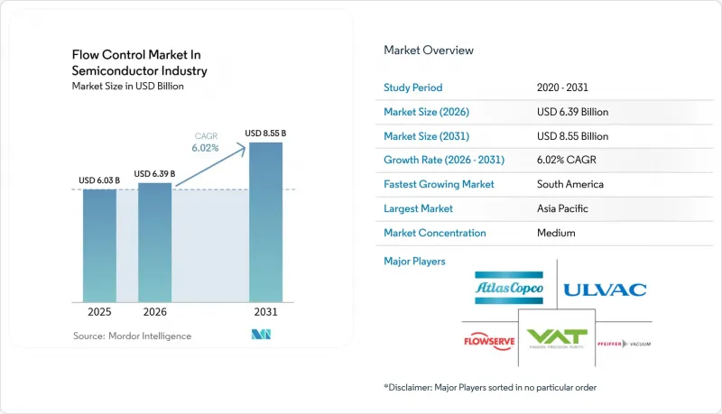
本報告按組件(真空系統、閥門、機械軸封等)、製程(薄膜沉積、蝕刻、離子布植、光刻等)、流體(氣體、液體)、潔淨度等級(高純度、標準純度)、閥門驅動方式(手動、氣動、電動)和地區進行細分。市場預測以美元(USD)為單位。
全球半導體產業流量控制市場的趨勢與洞察。
韓國和台灣的製造工廠對 EUV 光刻真空設備的需求呈現爆炸性成長。
隨著韓國和台灣的半導體製造商不斷擴大其極紫外光微影(EUV)產能,對超高真空流體處理系統的需求空前高漲。台積電向高數值孔徑(High-NA)EUV技術的轉型需要低於10⁻¹¹ Torr的真空度,並需要特殊的閥門配置來防止光阻劑加工過程中碳氫化合物的污染。三星的EUV藍圖在2026年部署15台新型EUV掃描儀,每台掃描儀都需要價值約200萬至300萬美元的專用流體處理基礎設施。這種技術複雜性源自於EUV對分子污染的極高敏感性;即使是微量的有機化合物也會降低鏡面反射率,進而降低光刻良率。
向 200 多層以上的 3D-NAND 的轉變正在推動對高流量 ALD 閥的需求(中國)。
隨著中國大力推動200層以上的3D-NAND技術,對能夠以前所未有的規模處理前驅體供應的高流量ALD閥的需求顯著成長。長江儲存(YMTC)正在開發的232層3D-NAND需要採用沉積速率超過50奈米/小時的ALD工藝,這就要求閥門系統的流量是傳統128層工藝的3到4倍。技術挑戰在於如何在300毫米晶圓上保持前驅體的均勻性,同時防止不同化學物質之間的交叉污染。中國製造商正在大力投資國內流體處理能力建設,以減少對海外供應商的依賴,例如NAURA和AMEC等公司正在開發自己的閥門技術。然而,中國超過80%的氟橡膠密封件依賴從日本和德國供應商進口,這使得高純度材料的採購成為這項轉型的主要障礙。
歐盟逐步淘汰 PFAS 的計畫推高了材料重新設計的成本。
歐盟計畫在2029年前淘汰4000種含氟化合物,這將迫使閥門製造商更換杜邦公司的Kalrez密封件及類似產品。歐洲企業表示,材料成本將上漲40%至80%,認證週期將延長至18至24個月,他們還必須遵守2025年4月生效的荷蘭出口限制。
細分市場分析
至2025年,閥門將佔半導體流體處理市場45.40%的佔有率。真空系統的銷售額正以6.95%的複合年成長率成長,因為極紫外光微影和先進封裝技術都依賴超高真空。
市場對洩漏率低於 10-12 mbar·L/s 的全金屬閘閥的需求正在迅速成長,VAT 和 Fujikin 在該領域處於領先地位。半導體流體處理真空系統市場預計將成長最快,這主要得益於採用磁軸承的新型乾式泵,其流量可達 2,000 l/s,平均故障間隔時間 (MTBF) 超過 50,000 小時。
供應商正擴大將閥門、泵浦和質量流量控制器整合到模組化撬裝設備中,從而將晶圓廠的安裝時間縮短 30%。智慧閥門內建的預測分析功能可提高產能並延長密封件壽命,從而降低晶圓廠營運商的整體擁有成本 (TCO)。研發重點正轉向符合 ISO-1 清潔度標準的無 PFAS 彈性體以及電解濕潤零件。
到 2025 年,薄膜沉積製程的銷售額佔比為 20.80%,而光刻技術的複合年成長率為 7.6%,並且正在成為半導體流體處理市場需求的最大驅動力。
原子層沉積 (ALD) 需要毫秒級到分鐘級的閥門切換,並將雜質控制在十億分之一的水平。應用材料公司的選擇性沉積平台需要快速切換前驅體,因此精密的閥組至關重要。同時,隨著高數值孔徑 (NA) EUV 微影技術的普及,用於微影術設備的半導體流體處理市場也不斷擴大,因為無污染的光阻劑管線直接影響良率。
蝕刻、離子布植和濕式清洗仍然至關重要,但市場已趨於成熟。這些領域的升級主要受產能提升的驅動。至於與自動化物料搬運相關的裝載鎖的升級,隨著300毫米自動化技術在旨在提高生產效率的200毫米晶圓廠中日益普及,相關投資也再次活躍起來。
區域分析
預計到2025年,以台灣和韓國為中心的亞太地區將佔據半導體流體處理市場33.60%的佔有率。台積電擴建九座晶圓廠以及三星擴大EUV光刻部署是推動需求成長的主要因素。儘管有出口限制,但中國市場預計仍將保持強勁成長,長江實業和中芯國際正在建立自身的供應鏈。日本在設備和材料方面的專業技術也支撐著對閥門和泵浦的高需求。北美市場正受惠於《晶片技術創新與應用法案》(CHIPS Act)。英特爾、美光和格羅方德的項目均需要價值1.5億至2億美元的流體系統,這形成了一個區域叢集,縮短了前置作業時間並增強了市場韌性。在歐洲市場,PFAS法規增加了材料重新設計的成本,但也為合規供應商帶來了競爭優勢。 ASML位於荷蘭的工廠持續收到針對EUV微影元件的客製訂單。
以巴西為首的南美洲正以7.55%的複合年成長率(CAGR)領跑,各國政府正積極吸引投資進入半導體組裝測試領域,以實現供應鏈多元化。儘管基礎設施和勞動力短缺仍然是挑戰,但有針對性的激勵措施以及與跨國公司的合作正逐步提升市場對模組化、低成本流體處理組件的需求,以滿足新興晶圓廠環境的需求。
其他好處:
- Excel格式的市場預測(ME)表
- 3個月的分析師支持
目錄
第1章:引言
- 研究假設和市場定義
- 調查範圍
第2章:調查方法
第3章執行摘要
第4章 市場狀況
- 市場概覽
- 市場促進因素
- 韓國和台灣的製造工廠對極紫外光刻真空設備的需求正在激增。
- 向 200 多層以上的 3D-NAND 的轉變正在推動對高流量 ALD 閥的需求(中國)。
- 美國《CHIPS法案》推動了製造業的擴張,進而帶動了對化學品分配閥的需求。
- 為符合 PFAS 排放法規,引進乾式真空幫浦(日本)
- 混合鍵合封裝需要精確的流量控制,全球範圍內小於 1 Torr。
- 面向預測性維護的工業物聯網智慧閥門(歐洲)
- 市場限制因素
- 歐盟逐步淘汰 PFAS 的計畫將增加材料重新設計的成本。
- 由於高純度氟橡膠供應短缺,密封件價格上漲。
- 南美洲對超高真空閥的資本投資需求阻礙了其廣泛應用。
- 與一級工具OEM廠商的認證週期為18-24個月
- 價值供應鏈分析
- 監理展望
- 技術展望
- 波特五力分析
第5章 市場規模與成長預測
- 按組件
- 真空系統
- 閥門
- 球閥
- 蝶閥
- 閘閥
- 球閥
- 其他
- 機械軸封
- 質量流量控制器
- 流量計
- 依工藝階段
- 薄膜形成(PVD/CVD/ALD)
- 蝕刻和乾剝離
- 離子布植
- 光刻
- 晶圓清洗和化學機械拋光
- 測量與檢驗
- 裝載鎖定和運輸
- 水處理和廢棄物處理
- 按流體類型
- 氣體
- 液體
- 清潔度等級
- 高純度(ISO 1-3)
- 標準純度(ISO 4+)
- 透過閥門驅動系統
- 手動的
- 氣動
- 電的
- 螺線管
- 按地區
- 北美洲
- 美國
- 加拿大
- 墨西哥
- 歐洲
- 德國
- 法國
- 荷蘭
- 英國
- 其他歐洲國家
- 亞太地區
- 中國
- 台灣
- 韓國
- 澳洲
- 日本
- 印度
- 東南亞
- 中東
- 以色列
- 沙烏地阿拉伯
- 阿拉伯聯合大公國
- 非洲
- 南非
- 其他非洲國家
- 南美洲
- 巴西
- 阿根廷
- 其他南美國家
- 北美洲
第6章 競爭情勢
- 市場集中度
- 策略性舉措(併購、合資、資金籌措)
- 市佔率分析
- 公司簡介
- Pfeiffer Vacuum GmbH
- Atlas Copco AB
- Gardner Denver(Ingersoll Rand)
- Flowserve Corporation
- Busch Holding GmbH
- Kurt J. Lesker Company
- ULVAC Inc.
- Edwards Vacuum Ltd.
- Ebara Corporation
- MKS Instruments Inc.
- INFICON Holding AG
- SMC Corporation
- VAT Vakuumventile AG
- Fujikin Incorporation
- GEMU Holding GmbH and Co. KG
- Swagelok Company
- Festo SE and Co. KG
- CKD Corporation
- Parker-Hannifin Corporation
- AESSEAL plc
- EKK Eagle Industry Co.
- DuPont de Nemours Inc.
- Freudenberg Group
- Greene Tweed and Co. Inc.
- Jordan Valve(Richards Industries)
第7章 市場機會與未來展望
According to Mordor Intelligence, flow control market size in semiconductor industry market size in 2026 is estimated at USD 6.39 billion, growing from 2025 value of USD 6.03 billion with 2031 projections showing USD 8.55 billion, growing at 6.02% CAGR over 2026-2031.
This report is Segmented by Component (Vacuum Systems, Valves, Mechanical Seals, and More), Process Step (Deposition, Etching, Ion Implantation, Lithography, and More), Flow Medium (Gases, Liquids), Cleanliness Rating (High-Purity, Standard-Purity), Valve Actuation Type (Manual, Pneumatic, Electric), and Geography. The Market Forecasts are Provided in Terms of Value (USD).
Global Flow Control in Semiconductor Industry Trends and Insights
Explosive EUV Lithography Vacuum Requirements in Korean and Taiwanese Fabs
Korean and Taiwanese semiconductor manufacturers are driving unprecedented demand for ultra-high vacuum fluid handling systems as they scale EUV lithography capacity. TSMC's transition to High-NA EUV technology requires vacuum levels below 10^-11 torr, demanding specialized valve configurations that prevent hydrocarbon contamination during photoresist processing. Samsung's EUV roadmap includes 15 new EUV scanners by 2026, each requiring dedicated fluid handling infrastructure worth approximately USD 2-3 million per tool. The technical complexity stems from EUV's sensitivity to molecular contamination, where even trace amounts of organic compounds can degrade mirror reflectivity and reduce lithography yield.
3D-NAND Transition Beyond 200 Layers Boosting High-Flow ALD Valves (China)
China's aggressive pursuit of 3D-NAND technology beyond 200 layers is creating substantial demand for high-flow atomic layer deposition valves capable of handling precursor delivery at unprecedented scales. YMTC's development of 232-layer 3D-NAND requires ALD processes with deposition rates exceeding 50 nm/hour, necessitating valve systems with flow rates 3-4 times higher than conventional 128-layer processes. The technical challenge lies in maintaining precursor uniformity across 300mm wafers while preventing cross-contamination between different chemical species. Chinese manufacturers are investing heavily in domestic fluid handling capabilities to reduce dependence on foreign suppliers, with companies like NAURA and AMEC developing indigenous valve technologies. However, the transition faces significant hurdles in high-purity material sourcing, as China imports over 80% of its fluoro-elastomer seals from Japanese and German suppliers.
EU PFAS Phase-Out Proposals Increasing Material Redesign Costs
EU plans to remove 4,000 fluorinated compounds by 2029, forcing valve makers to substitute DuPont Kalrez and similar seals. European firms report 40-80% higher material costs and 18-24 month qualification cycles while also navigating Dutch export controls effective April 2025.
Other drivers and restraints analyzed in the detailed report include:
- U.S. CHIPS Act Fab Build-out Raising Chemical-Distribution Valve Demand
- Dry Vacuum Pump Adoption to Meet PFAS-Emission Rules (Japan)
- Tight High-Purity Fluoro-Elastomer Supply Inflating Seal Prices
For complete list of drivers and restraints, kindly check the Table Of Contents.
Segment Analysis
Valves held 45.40% semiconductor fluid handling market share in 2025. Vacuum system revenue is rising at a 6.95% CAGR because EUV lithography and advanced packaging rely on ultra-high vacuum.
Demand for all-metal gate valves able to hold leak rates below 10-12 mbar*l/s grows quickly, with VAT and Fujikin leading adoption. The semiconductor fluid handling market size for vacuum systems is poised to expand fastest, supported by new dry pumps with magnetic bearings that reach 2,000 l/s and exceed 50,000 hours MTBF.
Suppliers increasingly bundle valves, pumps, and mass-flow controllers in modular skids that cut fab install time by 30%. Predictive analytics embedded in smart valves improve throughput and extend seal life, reducing total cost of ownership for fab operators. R&D focus has shifted toward PFAS-free elastomers and electropolished wetted paths that meet ISO-1 cleanliness.
Deposition processes generated 20.80% of 2025 revenue, while lithography is growing at 7.6% CAGR and becoming the fastest driver of semiconductor fluid handling market demand.
Atomic-layer deposition requires millisecond valve switching with parts-per-billion impurity control. Selective deposition platforms from Applied Materials must alternate precursors rapidly, necessitating advanced valve manifolds. Conversely, the semiconductor fluid handling market size for lithography tools increases alongside High-NA EUV because contamination-free photoresist lines directly impact yield.
Etch, ion implant, and wet clean remain essential but mature; upgrades here primarily follow capacity additions. Load-lock upgrades tied to automated material transfer are experiencing renewed investment as 300 mm automation spreads to 200 mm fabs seeking productivity gains.
Complete Report Scope:
- By Component
- Vacuum Systems
- Valves
- Ball
- Butterfly
- Gate
- Globe
- Other Valves
- Mechanical Seals
- Mass Flow Controllers
- Flow Meters
- By Process Step
- Deposition (PVD / CVD / ALD)
- Etching and Dry Strip
- Ion Implantation
- Lithography
- Wafer Cleaning and CMP
- Metrology and Inspection
- Load Lock and Transfer
- Water and Waste Treatment
- By Flow Medium
- Gases
- Liquids
- By Cleanliness Rating
- High-Purity (ISO 1-3)
- Standard-Purity (ISO 4+)
- By Valve Actuation Type
- Manual
- Pneumatic
- Electric
- Solenoid
- By Geography
- North America
- United States
- Canada
- Mexico
- Europe
- Germany
- France
- Netherlands
- United Kingdom
- Rest of Europe
- Asia-Pacific
- China
- Taiwan
- South Korea
- Australia
- Japan
- India
- Southeast Asia
- Middle East
- Israel
- Saudi Arabia
- United Arab Emirates
- Africa
- South Africa
- Rest of Africa
- South America
- Brazil
- Argentina
- Rest of South America
- North America
Geography Analysis
Asia-Pacific held 33.60% semiconductor fluid handling market share in 2025, anchored by Taiwan and South Korea. TSMC's nine-fab expansion and Samsung's EUV scale-up are foremost demand engines. China remains a colossal growth prospect despite export controls, with YMTC and SMIC building indigenous supply chains. Japan's equipment sector and materials expertise also sustain high valve and pump requirements. North America enjoys renewed momentum through the CHIPS Act. Intel, Micron, and GlobalFoundries projects each require USD 150-200 million in fluid systems, fostering regional clusters that shorten lead times and bolster resilience. Europe's market confronts PFAS restrictions that inflate material redesign costs yet also create competitive moats for compliant suppliers; ASML's Dutch base sustains specialized orders for EUV-ready components.
South America, led by Brazil, registers the fastest 7.55% CAGR as governments court semiconductor assembly and test investments to diversify supply chains. Infrastructure gaps and skills shortages remain hurdles but targeted incentives and multinational partnerships are stimulating incremental demand for modular, lower-cost fluid handling packages suited to emerging fab environments.
- Pfeiffer Vacuum GmbH
- Atlas Copco AB
- Gardner Denver (Ingersoll Rand)
- Flowserve Corporation
- Busch Holding GmbH
- Kurt J. Lesker Company
- ULVAC Inc.
- Edwards Vacuum Ltd.
- Ebara Corporation
- MKS Instruments Inc.
- INFICON Holding AG
- SMC Corporation
- VAT Vakuumventile AG
- Fujikin Incorporation
- GEMU Holding GmbH and Co. KG
- Swagelok Company
- Festo SE and Co. KG
- CKD Corporation
- Parker-Hannifin Corporation
- AESSEAL plc
- EKK Eagle Industry Co.
- DuPont de Nemours Inc.
- Freudenberg Group
- Greene Tweed and Co. Inc.
- Jordan Valve (Richards Industries)
Additional Benefits:
- The market estimate (ME) sheet in Excel format
- 3 months of analyst support
TABLE OF CONTENTS
1 INTRODUCTION
- 1.1 Study Assumptions and Market Definition
- 1.2 Scope of the Study
2 RESEARCH METHODOLOGY
3 EXECUTIVE SUMMARY
4 MARKET LANDSCAPE
- 4.1 Market Overview
- 4.2 Market Drivers
- 4.2.1 Explosive EUV Lithography Vacuum Requirements in Korean and Taiwanese Fabs
- 4.2.2 3D-NAND Transition Beyond 200 Layers Boosting High-Flow ALD Valves (China)
- 4.2.3 U.S. CHIPS Act Fab Build-out Raising Chemical-Distribution Valve Demand
- 4.2.4 Dry Vacuum Pump Adoption to Meet PFAS-Emission Rules (Japan)
- 4.2.5 Hybrid-Bonding Packaging Needs Sub-1 Torr Micro-Flow Controls (Global)
- 4.2.6 IIoT-Enabled Smart Valves for Predictive Maintenance (Europe)
- 4.3 Market Restraints
- 4.3.1 EU PFAS Phase-Out Proposals Increasing Material Redesign Costs
- 4.3.2 Tight High-Purity Fluoro-Elastomer Supply Inflating Seal Prices
- 4.3.3 Capex-Intensive Ultra-High-Vacuum Valves Limiting Adoption in South America
- 4.3.4 18-24 Month Qualification Cycles with Tier-1 Tool OEMs
- 4.4 Value / Supply-Chain Analysis
- 4.5 Regulatory Outlook
- 4.6 Technological Outlook
- 4.7 Porter's Five Forces Analysis
- 4.7.1 Bargaining Power of Suppliers
- 4.7.2 Bargaining Power of Buyers
- 4.7.3 Threat of New Entrants
- 4.7.4 Threat of Substitutes
- 4.7.5 Intensity of Rivalry
5 MARKET SIZE AND GROWTH FORECASTS (VALUE)
- 5.1 By Component
- 5.1.1 Vacuum Systems
- 5.1.2 Valves
- 5.1.2.1 Ball
- 5.1.2.2 Butterfly
- 5.1.2.3 Gate
- 5.1.2.4 Globe
- 5.1.2.5 Other Valves
- 5.1.3 Mechanical Seals
- 5.1.4 Mass Flow Controllers
- 5.1.5 Flow Meters
- 5.2 By Process Step
- 5.2.1 Deposition (PVD / CVD / ALD)
- 5.2.2 Etching and Dry Strip
- 5.2.3 Ion Implantation
- 5.2.4 Lithography
- 5.2.5 Wafer Cleaning and CMP
- 5.2.6 Metrology and Inspection
- 5.2.7 Load Lock and Transfer
- 5.2.8 Water and Waste Treatment
- 5.3 By Flow Medium
- 5.3.1 Gases
- 5.3.2 Liquids
- 5.4 By Cleanliness Rating
- 5.4.1 High-Purity (ISO 1-3)
- 5.4.2 Standard-Purity (ISO 4+)
- 5.5 By Valve Actuation Type
- 5.5.1 Manual
- 5.5.2 Pneumatic
- 5.5.3 Electric
- 5.5.4 Solenoid
- 5.6 By Geography
- 5.6.1 North America
- 5.6.1.1 United States
- 5.6.1.2 Canada
- 5.6.1.3 Mexico
- 5.6.2 Europe
- 5.6.2.1 Germany
- 5.6.2.2 France
- 5.6.2.3 Netherlands
- 5.6.2.4 United Kingdom
- 5.6.2.5 Rest of Europe
- 5.6.3 Asia-Pacific
- 5.6.3.1 China
- 5.6.3.2 Taiwan
- 5.6.3.3 South Korea
- 5.6.3.4 Australia
- 5.6.3.5 Japan
- 5.6.3.6 India
- 5.6.3.7 Southeast Asia
- 5.6.4 Middle East
- 5.6.4.1 Israel
- 5.6.4.2 Saudi Arabia
- 5.6.4.3 United Arab Emirates
- 5.6.5 Africa
- 5.6.5.1 South Africa
- 5.6.5.2 Rest of Africa
- 5.6.6 South America
- 5.6.6.1 Brazil
- 5.6.6.2 Argentina
- 5.6.6.3 Rest of South America
- 5.6.1 North America
6 COMPETITIVE LANDSCAPE
- 6.1 Market Concentration
- 6.2 Strategic Moves (M&A, JVs, Funding)
- 6.3 Market Share Analysis
- 6.4 Company Profiles (includes Global level Overview, Market level overview, Core Segments, Financials as available, Strategic Information, Market Rank/Share for key companies, Products and Services, and Recent Developments)
- 6.4.1 Pfeiffer Vacuum GmbH
- 6.4.2 Atlas Copco AB
- 6.4.3 Gardner Denver (Ingersoll Rand)
- 6.4.4 Flowserve Corporation
- 6.4.5 Busch Holding GmbH
- 6.4.6 Kurt J. Lesker Company
- 6.4.7 ULVAC Inc.
- 6.4.8 Edwards Vacuum Ltd.
- 6.4.9 Ebara Corporation
- 6.4.10 MKS Instruments Inc.
- 6.4.11 INFICON Holding AG
- 6.4.12 SMC Corporation
- 6.4.13 VAT Vakuumventile AG
- 6.4.14 Fujikin Incorporation
- 6.4.15 GEMU Holding GmbH and Co. KG
- 6.4.16 Swagelok Company
- 6.4.17 Festo SE and Co. KG
- 6.4.18 CKD Corporation
- 6.4.19 Parker-Hannifin Corporation
- 6.4.20 AESSEAL plc
- 6.4.21 EKK Eagle Industry Co.
- 6.4.22 DuPont de Nemours Inc.
- 6.4.23 Freudenberg Group
- 6.4.24 Greene Tweed and Co. Inc.
- 6.4.25 Jordan Valve (Richards Industries)
7 MARKET OPPORTUNITIES AND FUTURE OUTLOOK
- 7.1 White-Space and Unmet-Need Assessment

 IC逆向工程市場:全球市場預測,2026-2032年
 導線架市場報告:趨勢、預測與競爭分析(至2035年)半導體擴散設備市場:依產品類型、技術、晶圓尺寸、最終用戶、應用、國家及地區分類-全球產業分析、市場規模、市場佔有率及2026年至2033年預測半導體聚焦環市場:依產品類型、應用、最終用戶、國家及地區分類-全球產業分析、市場規模、市場佔有率及2026年至2033年預測半導體電鍍化學品市場:依產品類型、應用、材料、技術節點、最終用戶、國家及地區分類-全球產業分析、市場規模、市場佔有率及2026年至2033年預測
 基於晶片的半導體市場預測至2034年-按晶片類型、封裝技術、互連技術、製程節點、應用、最終用戶和地區分類的全球分析量子計算半導體市場預測至2034年—按組件、技術類型、材料、應用、最終用戶和地區分類的全球分析
 歐洲消費與工業半導體裝置:市場佔有率分析、產業趨勢與統計及成長預測(2025-2030 年)
 物聯網半導體市場規模、佔有率和成長分析:按產品類型、應用、連接標準和地區分類-2026-2033年產業預測
 用於替代能源技術的半導體:機會和市場