


 |
市場調查報告書
商品編碼
2099407
DRAM封裝產業的熱界面材料:市場佔有率分析、行業趨勢和統計數據以及成長預測(2026-2031年)Thermal Interface Materials For DRAM Packaging - Market Share Analysis, Industry Trends & Statistics, Growth Forecasts (2026 - 2031) |
||||||

※ 本網頁內容可能與最新版本有所差異。詳細情況請與我們聯繫。
據 Mordor Intelligence 稱,2025 年 DRAM 封裝行業的熱界面材料市場價值為 3.9 億美元,預計到 2031 年將從 2026 年的 4.9 億美元成長至 13.2 億美元,2026 年至 2031 年預測期內的複合成長率為 21.92%。
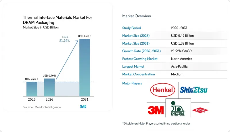
本報告材料類型(導熱油脂和導熱膏、導熱墊/間隙墊等)、DRAM封裝/產品應用(HBM堆疊、高級DRAM封裝、伺服器DRAM模組等)、終端應用平台(AI伺服器和加速器等)以及地區(北美等)進行細分。市場預測以美元計價。
DRAM封裝產業導熱介面材料的市場洞察與趨勢
HBM堆疊高度和D2D熱密度增加
DRAM封裝產業的導熱介面材質市場正直接回應堆疊式記憶體架構的興起,這種架構在較窄的垂直空間內整合了更多晶片。隨著HBM結構高度的增加,從下層晶片到封裝頂蓋的串聯熱阻也隨之增加,即使改進了外部散熱,散熱仍然困難。西門子EDA指出,HBM4的設計目標中堆疊高度和I/O密度都在增加,這加劇了晶片間(D2D)物理層的局部熱集中。 imec預測,到2025年,這項散熱挑戰將更加嚴峻,在不採取散熱措施的情況下,採用3D HBM-on-GPU配置時,GPU峰值溫度將達到141.7 度C,而2.5D基準配置的峰值溫度僅為69.1 度C。為此,SK海力士於2026年5月發布了iHBM解決方案,將散熱元件整合到D2D PHY區域。這種方法成功地將熱阻降低了30%,同時保持了與現有系統級封裝(SiP)結構的兼容性。因此,DRAM封裝產業的熱界面材料市場正轉向能夠支援更窄間隙、更穩定的鍵合線以及在封裝內多個界面位置實現更高導熱係數的材料。
向混合鍵合和熱協同最佳化過渡
隨著先進記憶體組件中熱壓鍵合技術向混合銅鍵合技術的轉變,DRAM封裝產業的導熱介面材料市場格局也正在重塑。這種轉變改變了熱量的積聚位置,以及材料選擇對封裝完整性和散熱性能的影響。發表於《Electronics in 2025》的一篇綜述報導指出,SiCN介電材料、奈米孿晶銅和聚合物複合材料在熱阻、翹曲控制和熱膨脹係數不匹配方面各有優劣。 Imec的跨技術協同最佳化研究表明,將技術和系統冷卻決策作為一個整體進行建模,而不是單獨建模,可以使混合鍵合的3D系統更接近2.5D的熱行為。這項進展導致產品需求細分為不同的領域:堆疊內部材料和蓋板介面材料,從而催生了更專業的供應商產品系列。從實際角度來看,DRAM封裝產業的導熱介面材料市場正在轉變採購策略,從單一材料選擇轉向更廣泛的封裝級散熱設計決策。
高性能填料和樹脂原料所帶來的成本壓力
DRAM封裝產業的導熱介面材料市場正面臨來自高性能配方中使用的高品質填料和矽載體系統的巨大成本壓力。 2026年4月,信越化學宣布,由於中東供應狀況導致原油和石腦油價格上漲,公司將把所有矽產品的價格上調10%以上。這對DRAM封裝產業影響巨大,因為矽系統仍佔據認證材料的大部分佔有率。在薄鍵合線領域,這種影響更為顯著,因為需要高純度、嚴格控制的填料系統才能在緊湊的結構中保持穩定的性能。雖然大型供應商可以透過規模經濟和廣泛的採購網路來緩解部分壓力,但小型配方製造商的利潤空間有限。因此,在DRAM封裝產業的導熱介面材料市場,不斷上漲的原料成本正在增強現有企業的競爭優勢,而下一代產品則需要更專業的原料。
細分市場分析
2025年,導熱墊/間隙墊在DRAM封裝產業的導熱介面材料市場中仍佔據重要地位,市佔率高達34.67%。其強勁的市場地位源自於其在伺服器DRAM模組和企業級記憶體系統中的成熟應用,在這些應用中,穩定的鍵合線控制和易於操作至關重要。此外,這些產品也非常適合自動化組裝流程,並且相比其他一些替代形式,它們能夠更快速地回應返工需求。這些優勢確保了即使封裝要求日益複雜,基於墊片的產品在傳統DRAM模組組裝中仍然佔據核心地位。 DRAM封裝的導熱介面材料市場將繼續依賴這些產品,因為可製造性、成熟的應用經驗以及峰值導熱性是其最重要的考慮因素。
預計到2031年,導熱凝膠和與點膠器相容的間隙填充劑將以22.15%的複合年成長率成長,這反映出它們更適用於HBM堆疊和基於2.5D中介層的封裝中更緊湊的界面形狀。陶氏化學將於2026年5月推出DOWSIL TC-3120導熱凝膠,顯示供應商正在將可點膠材料定位為減少油滲和冷凝脫氣,以用於高密度、高速電子產品。相變材料也因其能夠降低重複循環過程中泵出的風險,在蓋板界面處越來越受歡迎。雖然潤滑脂和膏狀物仍在傳統伺服器平台中使用,但在先進節點中,由於鍵合線的變異性和遷移風險是不可接受的,因此對它們的採用要求越來越嚴格。 「其他」類別目前在銷售額中仍然小規模,但由於碳基、石墨基和其他新型材料有可能解決標準聚合物基材料性能不足的界面區域,因此正引起人們的關注。
區域分析
到2025年,亞太地區將佔據DRAM封裝產業導熱介面材料市場82.67%的佔有率,鞏固其作為全球需求中心的地位。這種集中度反映了DRAM生產、HBM組裝以及先進半導體代工組裝和測試(OEM)能力在韓國、台灣、日本和中國的地理集群。韓國仍然是最重要的市場,三星電子和SK海力士不僅擁有大規模的HBM生產能力,還直接參與下一代封裝的散熱設計。 SK海力士計劃於2026年推出iHBM,這表明該地區的記憶體製造商正在塑造封裝架構以及對周邊介面材料的要求。台灣憑藉其先進的封裝生態系統,其重要性日益凸顯。由於基於中介層的組裝和共封裝結構,需要管理的對熱敏感的介面數量正在增加。
日本透過供應高純度材料和開展記憶體相關封裝業務,為DRAM封裝產業的導熱介面材料市場提供支援。同時,中國正透過其國內OSAT(外包封裝組裝)企業的成長和在地化努力,不斷擴大其市場佔有率。然而,亞太地區在某些高階應用領域,尤其是在需要特殊填料系統和低釋氣量的領域,仍依賴進口高性能複合材料。預計到2031年,北美市場將以22.87%的複合年成長率成長,成為成長最快的地區市場。這一成長主要得益於對人工智慧基礎設施的投資、超大規模超大規模資料中心業者營運商的客製化認證需求以及對國內半導體產能的政策支援。 Carvice與DarkNX於2026年2月達成的合作,以及與美國海軍於2026年4月簽署的認證協議,都體現了北美供應商瞄準高階溫度控管領域,這些領域需要高可靠性和特定應用檢驗。
北美市場的需求著重於認證、部署和性能保證,而非大規模DRAM晶片生產,這提高了每種認證材料的附加價值。歐洲在DRAM封裝產業的導熱介面材料市場中保持著雖小但穩定的佔有率,這主要得益於企業資料中心的需求和專業工業運算應用。歐洲客戶優先考慮符合規範的配方,對無矽和低釋氣產品的興趣依然濃厚。雖然世界其他地區的銷售額仍然較小,但東南亞和印度的封裝市場正在成長,隨著區域電子製造業的擴張,它們的重要性可能會進一步提升。
其他好處:
- Excel格式的市場預測(ME)表
- 3個月的分析師支持
目錄
第1章:引言
- 研究假設和市場定義
- 調查範圍
第2章:調查方法
第3章執行摘要
第4章 市場狀況
- 市場概覽
- 宏觀經濟因素對市場的影響
- 市場促進因素
- HBM堆疊高度增加,D2D熱密度提高
- 向混合鍵合和熱協同最佳化過渡
- 每個系統的AI伺服器記憶體容量增加
- 企業級記憶體系統 24/7 全天候運作的可靠性要求。
- 對超薄界面間隙高導熱性的需求
- 合格於不含矽油且低揮發性導熱界面材料配方。
- 市場限制因素
- 優質填料和樹脂原料帶來的成本壓力
- 最先進的DRAM封裝生產線的認證風險
- 基板翹曲和製程窗口變窄
- 整合冷卻和封裝級熱設計帶來的競爭力
- 產業價值鏈分析
- 監理情勢
- 技術展望
- 波特五力分析
第5章 市場規模與成長預測
- 依材料類型
- 導熱油脂和膏
- 相變材料
- 熱凝膠/適用縫隙填充劑
- 導熱墊/間隙墊
- 其他(石墨/碳基導熱界面材料、先進奈米複合材料導熱界面材料)
- DRAM封裝類型/產品應用
- HBM堆疊
- 高級DRAM封裝
- 伺服器 DRAM 模組
- 客戶-向け DRAM模組
- CXL連接的DRAM模組
- 按最終用戶平台
- AI伺服器和加速器
- 高效能運算
- 企業級和超大規模資料中心
- 高階工作站
- 用戶端桌上型電腦和筆記型電腦
- 工業與嵌入式運算
- 按地區
- 北美洲
- 歐洲
- 亞太地區
- 中國
- 日本
- 韓國
- 台灣
- 其他亞太國家
- 世界其他地區
第6章 競爭情勢
- 市場集中度
- 策略趨勢
- 市佔率分析
- 公司簡介
- 3M
- Henkel AG and Co. KGaA
- The Dow Chemical Company
- Shin-Etsu Chemical Co., Ltd.
- Indium Corporation
- Parker-Hannifin Corporation
- Laird Thermal Systems, Inc.
- Henkel Adhesive Technologies
- Fujipoly, a division of Fuji Polymer Industries Co., Ltd.
- Momentive Performance Materials Inc.
- Boyd Corporation
- Momentive Technologies
- DuPont de Nemours, Inc.
- Wacker Chemie AG
- Honeywell International Inc.
- Saint-Gobain SA
- Aavid Thermalloy, LLC
- Wakefield-Vette, Inc.
- Carbice Corporation
- Fujipoly America Corporation
第7章 市場機會與未來展望
According to Mordor Intelligence, the thermal interface materials market for DRAM packaging industry size was valued at USD 0.39 billion in 2025 and is estimated to grow from USD 0.49 billion in 2026 to reach USD 1.32 billion by 2031, at a CAGR of 21.92% during the forecast period 2026-2031.
This report is Segmented by Material Type (Thermal Greases and Pastes, Thermal Pads / Gap Pads, and More), DRAM Packaging / Product Application (HBM Stacks, Advanced DRAM Packages, Server DRAM Modules, and More), End-Use Platform (AI Servers and Accelerators, and More), and Geography (North America, and More). The Market Forecasts are Provided in Terms of Value (USD).
Insights and Trends of Thermal Interface Materials Market For DRAM Packaging
Rising HBM Stack Height and D2D Heat Density
The thermal interface materials market for DRAM packaging industry is responding directly to the rise in stacked memory architectures, where more dies are being placed within tighter vertical limits. Taller HBM structures increase serial thermal resistance from the lower dies to the package lid, which makes heat removal harder even when external cooling improves. Siemens EDA noted that HBM4 design targets raise both stack height and I/O density, which increases localized heat concentration in the die-to-die physical layer. Imec showed the scale of this thermal challenge in 2025, reporting a peak GPU temperature of 141.7°C in a 3D HBM-on-GPU setup without mitigation, versus 69.1°C in a 2.5D baseline. SK hynix responded in May 2026 by introducing its iHBM solution with integrated cooling elements in the D2D PHY area, which cut thermal resistance by 30% while staying compatible with existing System-in-Package structures. As a result, the thermal interface materials market for DRAM packaging industry is moving toward materials that can support tighter gaps, more stable bond lines, and higher conductivity at multiple interface positions inside the package.
Shift To Hybrid Bonding and Thermal Co-Optimization
The thermal interface materials market for DRAM packaging industry is also being reshaped by the move from thermal compression bonding toward hybrid copper bonding in advanced memory assembly. This shift changes where heat builds up and how material selection affects both package integrity and thermal performance. A 2025 review in Electronics described how SiCN dielectrics, nano-twinned copper, and polymer composites each bring different tradeoffs in thermal resistance, warpage control, and coefficient of thermal expansion mismatch. Imec's cross-technology co-optimization work showed that hybrid-bonded 3D systems can move closer to 2.5D thermal behavior when technology and system cooling decisions are modeled together, not in isolation. That development is splitting product demand into separate tracks for intra-stack materials and lid-interface materials, which makes supplier portfolios more specialized. In practical terms, the thermal interface materials market for DRAM packaging industry is seeing procurement shift from a single material decision toward a broader package-level thermal design decision.
Cost Pressure from Premium Filler And Resin Inputs
The thermal interface materials market for DRAM packaging industry faces clear cost pressure from premium fillers and silicone-based carrier systems used in high-performance formulations. Shin-Etsu announced in April 2026 that it would raise prices on all silicone products by 10% or more, citing crude oil and naphtha cost increases linked to Middle East supply conditions. That matters because silicone-based systems still account for much of the qualified material base in DRAM packaging. The effect is stronger in thinner bond lines, where high-purity and tightly controlled filler systems are needed to keep performance stable in compact geometries. Larger suppliers can absorb some of this pressure through scale and broader sourcing networks, while smaller formulators have less room to protect margins. As a result, the thermal interface materials market for DRAM packaging industry is seeing higher input costs reinforce incumbent strength at the same time that next-generation products require more specialized ingredients.
Other drivers and restraints analyzed in the detailed report include:
- Expansion of AI Server Memory Content Per System
- Reliability Requirements In 24/7 Enterprise Memory Systems
- Qualification Risk in Advanced DRAM Packaging Lines
For complete list of drivers and restraints, kindly check the Table Of Contents.
Segment Analysis
Thermal pads/gap pads held 34.67% of the thermal interface materials market for DRAM packaging industry share in 2025, which kept them as the leading material category. Their strong position came from established use in server DRAM modules and enterprise memory systems, where consistent bond-line control and easier handling remained valuable. They also fit well with automated assembly flows and support rework needs better than several alternative formats. That combination kept pad-based products central to conventional DRAM module assembly even as packaging demands became more complex. The thermal interface materials for DRAM packaging market still relies on these formats where manufacturability and qualification history matter as much as peak conductivity.
Thermal gels and dispensable gap fillers are forecast to grow at a 22.15% CAGR through 2031, reflecting their better fit with tighter interface geometries in HBM stacks and 2.5D interposer-based packages. Dow's launch of DOWSIL TC-3120 Thermal Gel in May 2026 showed how suppliers are positioning dispensable chemistries for dense, high-speed electronics with lower oil bleeding and lower condensed outgassing. Phase change materials are also gaining ground in lid-interface positions because they reduce pump-out risk during repeated cycling. Greases and pastes continue to serve conventional server platforms, but they face more pressure in advanced nodes where bond-line variation and migration risk are less acceptable. The Others category remains small in current revenue, yet it is drawing attention because carbon-based, graphite-based, and other novel materials could address interface positions that standard polymer systems serve less effectively.
Complete Report Scope:
- By Material Type
- Thermal Greases and Pastes
- Phase Change Materials
- Thermal Gels / Dispensable Gap Fillers
- Thermal Pads / Gap Pads
- Others (Graphite / Carbon-Based TIMs, Advanced Nano-Composite TIMs)
- By DRAM Packaging / Product Application
- HBM Stacks
- Advanced DRAM Packages
- Server DRAM Modules
- Client DRAM Modules
- CXL Attached DRAM Modules
- By End-Use Platform
- AI Servers and Accelerators
- High-Performance Computing
- Enterprise and Hyperscale Data Centers
- High-End Workstations
- Client PCs and Notebooks
- Industrial and Embedded Computing
- By Geography
- North America
- Europe
- Asia-Pacific
- China
- Japan
- South Korea
- Taiwan
- Rest of Asia-Pacific
- Rest of the World
Geography Analysis
Asia-Pacific held 82.67% of the thermal interface materials market for DRAM packaging industry market share in 2025, which made the region the clear center of global demand. This concentration reflects the geographic clustering of DRAM production, HBM assembly, and advanced outsourced semiconductor assembly and test capacity across South Korea, Taiwan, Japan, and China. South Korea remains the most important country position because Samsung Electronics and SK hynix combine large HBM output with direct involvement in next-generation package thermal design. SK hynix's 2026 iHBM launch shows how memory producers in the region are shaping both package architecture and the interface material requirements that sit around it. Taiwan adds further weight through its advanced packaging ecosystem, where interposer-based assembly and co-packaged structures increase the number of thermally sensitive interfaces that must be managed.
Japan supports the thermal interface materials market for DRAM packaging industry through high-purity materials supply and memory-related packaging operations, while China is expanding its position through domestic OSAT growth and localization efforts. At the same time, Asia-Pacific still depends on imported high-performance formulations in some premium applications, especially where specialized filler systems or low-outgassing behavior are required. North America is forecast to grow at a 22.87% CAGR through 2031, which makes it the fastest-rising regional market. This growth is being driven by AI infrastructure investment, custom qualification needs from hyperscalers, and policy support for domestic semiconductor capacity. Carbice's partnership with DarkNX in February 2026 and its U.S. Navy qualification contract in April 2026 reflect how North American suppliers are targeting premium thermal positions that require high reliability and application-specific validation.
Demand in North America is concentrated more in qualification, deployment, and performance assurance than in large-scale DRAM die production, which lifts value intensity per approved material. Europe remains a smaller but stable part of the thermal interface materials market for DRAM packaging industry, supported by enterprise data center demand and specialized industrial computing uses. European customers place greater emphasis on compliance-sensitive formulations, which keeps interest high in silicone-free and low-outgassing products. The Rest of the World remains a smaller revenue pool, but countries in Southeast Asia and India could add relevance as packaging ambitions grow and regional electronics manufacturing broadens.
- 3M
- Henkel AG and Co. KGaA
- The Dow Chemical Company
- Shin-Etsu Chemical Co., Ltd.
- Indium Corporation
- Parker-Hannifin Corporation
- Laird Thermal Systems, Inc.
- Henkel Adhesive Technologies
- Fujipoly, a division of Fuji Polymer Industries Co., Ltd.
- Momentive Performance Materials Inc.
- Boyd Corporation
- Momentive Technologies
- DuPont de Nemours, Inc.
- Wacker Chemie AG
- Honeywell International Inc.
- Saint-Gobain S.A.
- Aavid Thermalloy, LLC
- Wakefield-Vette, Inc.
- Carbice Corporation
- Fujipoly America Corporation
Additional Benefits:
- The market estimate (ME) sheet in Excel format
- 3 months of analyst support
TABLE OF CONTENTS
1 INTRODUCTION
- 1.1 Study Assumptions and Market Definition
- 1.2 Scope of the Study
2 RESEARCH METHODOLOGY
3 EXECUTIVE SUMMARY
4 MARKET LANDSCAPE
- 4.1 Market Overview
- 4.2 Impact of Macroeconomic Factors on the Market
- 4.3 Market Drivers
- 4.3.1 Rising HBM Stack Height and D2D Heat Density
- 4.3.2 Shift to Hybrid Bonding and Thermal Co-Optimization
- 4.3.3 Expansion of AI Server Memory Content Per System
- 4.3.4 Reliability Requirements in 24/7 Enterprise Memory Systems
- 4.3.5 High Thermal Conductivity Demand in Ultra-Thin Interface Gaps
- 4.3.6 Qualification of Silicone-Free and Low-Outgassing TIM Formulations
- 4.4 Market Restraints
- 4.4.1 Cost Pressure from Premium Filler and Resin Inputs
- 4.4.2 Qualification Risk in Advanced DRAM Packaging Lines
- 4.4.3 Substrate Warpage and Process Window Narrowing
- 4.4.4 Competition from Integrated Cooling and Package-Level Thermal Designs
- 4.5 Industry Value Chain Analysis
- 4.6 Regulatory Landscape
- 4.7 Technological Outlook
- 4.8 Porter's Five Forces Analysis
- 4.8.1 Bargaining Power of Suppliers
- 4.8.2 Bargaining Power of Buyers
- 4.8.3 Threat of New Entrants
- 4.8.4 Threat of Substitutes
- 4.8.5 Competitive Rivalry
5 MARKET SIZE AND GROWTH FORECASTS (VALUE)
- 5.1 By Material Type
- 5.1.1 Thermal Greases and Pastes
- 5.1.2 Phase Change Materials
- 5.1.3 Thermal Gels / Dispensable Gap Fillers
- 5.1.4 Thermal Pads / Gap Pads
- 5.1.5 Others (Graphite / Carbon-Based TIMs, Advanced Nano-Composite TIMs)
- 5.2 By DRAM Packaging / Product Application
- 5.2.1 HBM Stacks
- 5.2.2 Advanced DRAM Packages
- 5.2.3 Server DRAM Modules
- 5.2.4 Client DRAM Modules
- 5.2.5 CXL Attached DRAM Modules
- 5.3 By End-Use Platform
- 5.3.1 AI Servers and Accelerators
- 5.3.2 High-Performance Computing
- 5.3.3 Enterprise and Hyperscale Data Centers
- 5.3.4 High-End Workstations
- 5.3.5 Client PCs and Notebooks
- 5.3.6 Industrial and Embedded Computing
- 5.4 By Geography
- 5.4.1 North America
- 5.4.2 Europe
- 5.4.3 Asia-Pacific
- 5.4.3.1 China
- 5.4.3.2 Japan
- 5.4.3.3 South Korea
- 5.4.3.4 Taiwan
- 5.4.3.5 Rest of Asia-Pacific
- 5.4.4 Rest of the World
6 COMPETITIVE LANDSCAPE
- 6.1 Market Concentration
- 6.2 Strategic Moves
- 6.3 Market Share Analysis
- 6.4 Company Profiles (includes Global Level Overview, Market Level Overview, Core Segments, Financials as available, Strategic Information, Market Rank/Share, Products and Services, Recent Developments)
- 6.4.1 3M
- 6.4.2 Henkel AG and Co. KGaA
- 6.4.3 The Dow Chemical Company
- 6.4.4 Shin-Etsu Chemical Co., Ltd.
- 6.4.5 Indium Corporation
- 6.4.6 Parker-Hannifin Corporation
- 6.4.7 Laird Thermal Systems, Inc.
- 6.4.8 Henkel Adhesive Technologies
- 6.4.9 Fujipoly, a division of Fuji Polymer Industries Co., Ltd.
- 6.4.10 Momentive Performance Materials Inc.
- 6.4.11 Boyd Corporation
- 6.4.12 Momentive Technologies
- 6.4.13 DuPont de Nemours, Inc.
- 6.4.14 Wacker Chemie AG
- 6.4.15 Honeywell International Inc.
- 6.4.16 Saint-Gobain S.A.
- 6.4.17 Aavid Thermalloy, LLC
- 6.4.18 Wakefield-Vette, Inc.
- 6.4.19 Carbice Corporation
- 6.4.20 Fujipoly America Corporation
7 MARKET OPPORTUNITIES AND FUTURE OUTLOOK
- 7.1 White-Space and Unmet-Need Assessment

 2026年全球分離式功率電子市場報告2026年全球功率半導體市場報告
 汽車智慧功率元件市場:依產品類型、應用、車輛類型、國家及地區分類-全球產業分析、市場規模、市場佔有率及2026年至2033年預測
 世界功率半導體市場、材料與技術
 功率半導體:市場佔有率分析、產業趨勢與統計、成長預測(2026-2031)分離式功率電子市場:按應用、類型、最終用途、技術、國家和地區分類-全球產業分析、市場規模、市場佔有率及2026年至2033年預測汽車智慧功率元件市場:全球產業分析、市場規模及佔有率和預測(2026-2033 年),按元件整合度、額定功率、應用、電壓範圍、國家和地區分類藍寶石功率元件市場:全球產業分析、市場規模、市場佔有率及2026年至2033年預測(依元件類型、應用、最終用戶、國家及地區分類)
 功率半導體市場:2026-2032年全球市場預測(依元件類型、材料、電壓範圍、晶圓尺寸、終端用戶產業及通路分類)
 功率半導體市場預測至2034年-按裝置類型、材料類型、封裝類型、應用和地區分類的全球分析