


 |
市場調查報告書
商品編碼
2066588
高速記憶體:市場佔有率分析、產業趨勢與統計資料、成長預測(2026-2031)High Bandwidth Memory - Market Share Analysis, Industry Trends & Statistics, Growth Forecasts (2026 - 2031) |
||||||

※ 本網頁內容可能與最新版本有所差異。詳細情況請與我們聯繫。
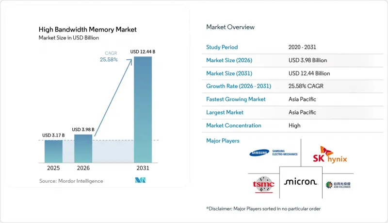
根據 Mordor Intelligence 預測,寬頻記憶體市場預計將從 2025 年的 31.7 億美元成長到 2026 年的 39.8 億美元,到 2031 年達到 124.4 億美元,2026 年至 2031 年的複合年預計成長率為 25.58%。
本報告按應用領域(伺服器、網路、高效能運算、家用電子電器、汽車與運輸)、技術(HBM2、HBM2E、HBM3、HBM3E、HBM4)、單棧記憶體容量(4 GB、8 GB、16 GB、24 GB 及以上)、處理器介面(GPU、CPU、AI 加速器/ASIC、FP 及其地區進行細分。市場預測以美元計價。
全球寬頻記憶體市場趨勢及洞察
AI伺服器的激增和搭載率。
企業正向GPU高密度伺服器遷移,這些伺服器每個節點需要4到8個HBM堆疊才能支援參數超過1兆的變壓器模型。戴爾科技集團報告稱,2025會計年度其AI最佳化伺服器的銷量年增80%,顯示傳統OEM廠商正從這項轉變中受益。像IREN這樣的非傳統買家(該公司從比特幣礦工轉型為AI提供商)已訂購了2萬塊Nvidia H200 GPU,每塊GPU配備141GB HBM3E顯存,這證實了頻寬需求正在各個行業蔓延。隨著模型尺寸的擴大,記憶體與運算能力的比率持續上升,為HBM供應商提供了未來幾年強勁的需求前景。雖然從HBM2E到HBM3E的過渡使每個堆疊的頻寬提高了50%,但開發人員已經在為2027年的硬體指定使用HBM4,這將縮短產品生命週期並導致研發工作重疊。因此,DRAM 製造商在系統物料清單 (BOM) 中所佔的佔有率比 GPU 供應商最初預期的要大。
資料中心向DDR5和2.5D封裝過渡
從DDR4到DDR5的過渡使基板和組裝製造商熟悉了吉赫訊號傳輸,從而降低了與HBM認證相關的認知風險。至2025年底,DDR5模組將佔伺服器DRAM出貨量的一半以上,而6.4 GT/s介面散熱設計的學習曲線也直接惠及HBM封裝。台積電的「晶片封裝在晶圓基板上(COWS)」製程在邏輯晶片和記憶體晶片之間佈線數千個微凸塊,這項技術源自於早期的2.5D現場可程式閘陣列(FPGA)。隨著製造技術的成熟,HBM的成本溢價已從通用DRAM的10倍縮小到約4倍,這促使其應用範圍從超大規模人工智慧擴展到高效能運算和高階顯示卡領域。標準化組織正在定義互通性,防止廠商鎖定,並加速高頻寬記憶體 (HBM) 在多個運算領域的應用。
CoWoS/SoIC先進封裝產能的限制
台積電的CoWoS和SoIC生產線預計到2025年底月產能將達到約12萬片晶圓,但英偉達一家就預定了2026年超過一半的產能。日月光、安靠和江森自控提供的扇出型封裝和矽橋接方案作為短期替代方案,但這些製程在良率和客戶認證方面仍存在不足,迫使中型晶片設計公司接受更長的檢驗週期和性能下降。台積電已將2026會計年度440億至500億美元的資本支出中的一部分用於擴大亞利桑那州的新封裝產能,但短期供應仍缺乏彈性。因此,到2028年,寬頻記憶體(HBM)市場成長的阻礙因素將是封裝產能,而非晶圓供應,採用多源策略的客戶將獲得優先配額。
細分市場分析
到2025年,伺服器將佔總銷售額的67.80%,成為寬頻記憶體市場的核心,預計該市場規模將達到31.7億美元。超大規模資料中心每個GPU將使用4到8個HBM堆疊,這意味著每年潛在的需求量將達到數百Petabyte。諸如800Gb乙太網路卡之類的網路設備正在採用HBM來滿足超低延遲的要求,但這僅佔銷售額的一小部分。高效能運算中心正在從HBM2E遷移到HBM3E,以縮短記憶體受限演算法解決方案的部署時間。
汽車平台是成長最快的領域,年複合成長率高達 26.58%,這得益於感測器融合和路徑規劃功能被整合到具有整合 HBM 的單一 SoC 上。 NVIDIA 的「Drive Thor」採用封裝整合 HBM,運算能力達到 2000 TOPS,每小時可處理約 1 TB 的感測器資料。堆疊式 DRAM 仍然是高階消費級顯示卡的主流,但 GDDR 則更受注重成本的 SKU 青睞,因為遊戲工作負載對頻寬的限制相對較小。從策略角度來看,汽車產業長期採用的設計方案,加上嚴格的安全認證,比超大規模資料中心領域的產品更新周期更能帶來更高的利潤率。
預計到2025年,HBM3將佔市場佔有率的45.70%,這主要得益於其在高效能運算和人工智慧應用中的廣泛應用。然而,HBM3E預計將以26.43%的成長率引領市場,因為供應商擴大認證性能超過3 TB/s的12層堆疊結構。這些先進的堆疊結構提供顯著更高的頻寬,從而減少了每個加速器所需的封裝數量。因此,中介層面積得以最小化,並提高了整體良率。同時,HBM2和HBM2E的市佔率正穩定下降,目前其應用主要局限於網路和傳統運算系統。
HBM4 樣品出貨於 2025 年初開始,標誌著儲存技術領域的一個重要里程碑。 SK 海力士率先出貨 12 層模組,三星緊追在後,僅數月後。 HBM4 擁有卓越的規格,單引腳傳輸速率超過 10 Gb/s,堆疊頻寬超過 2 TB/s。此外,與 HBM3E 相比,HBM4 的能源效率提升了 40%,使其成為次世代應用程式極具吸引力的選擇。預計量產將於 2026 年開始,並有望在 2020 年代末期加速 HBM4 在銷售構成比中的佔比提升。這一發展趨勢預計也將為光電賦能的 HBM 變體鋪平道路,這些變體預計將在 2028 年至 2029 年間問世。
區域分析
亞太地區是寬頻記憶體市場的主要驅動力,預計到2025年將佔據41.00%的市場佔有率,並在2031年之前以26.66%的複合年成長率持續成長。該地區受惠於韓國和日本等國的政府補貼,這些補貼使晶圓廠成本降低了20%至40%。這些補貼使得SK海力士等公司在第一季實現了72%的營業利潤率和371億美元的銷售額。此外,美光公司投資96億美元在廣島新建工廠,以實現供應鏈多元化,擺脫對中國市場的依賴,並確保供應鏈的穩定性。同時,中國國內DRAM製造商正努力在2026年前擴大HBM3的產能,但在技術進步和產能方面,仍落後於現有主要廠商18至24個月。
北美是全球第二大市場,這主要得益於超大規模資料中心業者的強勁需求以及政府透過《晶片創新與生產法案》(CHIPS Act)提供的大力津貼。這些總額超過66億美元的津貼在台積電位於亞利桑那州的先進封裝工廠的建設中發揮了至關重要的作用。英偉達、AMD和博通等美國主要公司佔據了全球HBM採購量的70%以上,該地區的供應鏈與矽谷的技術藍圖緊密契合。另一方面,由於國內DRAM產能有限,歐洲市場發展也相對落後。然而,歐洲仍然是一個重要的消費市場,尤其是在高級駕駛輔助系統(ADAS)和高效能運算(HPC)中心等應用領域。
南美、中東和非洲是新興市場的統稱,這些市場的需求正在不斷成長,主要受各國通訊基礎設施升級和人工智慧發展舉措的推動。然而,這些地區面臨出口許可限制和本地包裝能力不足等挑戰,短期內限制了出貨量。因此,這些市場目前更被視為未來成長的策略機遇,而非短期內的主要收入來源。
其他好處:
- Excel格式的市場預測(ME)表
- 3個月的分析師支持
目錄
第1章:引言
- 研究假設和市場定義
- 調查範圍
第2章:調查方法
第3章執行摘要
第4章 市場狀況
- 市場概覽
- 市場促進因素
- AI伺服器的激增和搭載率。
- 資料中心向DDR5和2.5D封裝的遷移
- 邊緣人工智慧推理在汽車高階駕駛輔助系統的應用
- 超大規模資料中心業者中心對矽中介層堆疊的偏好
- 對本地記憶體生產的補貼(韓國、美國、日本)
- 光電相容型 HBM (HBM-P)藍圖
- 市場限制因素
- 堆疊 12 層或更多層時,TSV 良率降低。
- CoWoS/SoIC先進封裝產能的限制
- 頻寬超過 1 TB/s 的設備會出現過熱降頻現象。
- 地緣政治對人工智慧加速器的出口限制
- 產業價值鏈分析
- 監理情勢
- 技術展望
- 波特五力分析
- DRAM市場分析
- DRAM 收入和需求預測
- 按地區分類的DRAM銷售額
- DDR5產品當前價格趨勢
- DDR5產品製造商列表
- 宏觀經濟因素的影響
第5章 市場規模與成長預測
- 透過使用
- 伺服器
- 網路
- 高效能運算
- 家用電子產品
- 汽車和運輸業
- 透過技術
- HBM2
- HBM2E
- HBM3
- HBM3E
- HBM4
- 每個堆疊的記憶體容量
- 4 GB4 GB
- 8 GB8 GB
- 16 GB16 GB
- 24 GB
- 32 GB 或更多
- 透過處理器介面
- GPU
- CPU
- 人工智慧加速器/專用積體電路
- FPGA
- 其他
- 按地區
- 北美洲
- 美國
- 加拿大
- 墨西哥
- 南美洲
- 巴西
- 其他南美國家
- 歐洲
- 德國
- 法國
- 英國
- 其他歐洲國家
- 亞太地區
- 中國
- 日本
- 印度
- 韓國
- 其他亞太國家
- 中東和非洲
- 中東
- 沙烏地阿拉伯
- 阿拉伯聯合大公國
- 土耳其
- 其他中東國家
- 非洲
- 南非
- 其他非洲國家
- 中東
- 北美洲
第6章 競爭情勢
- 市場集中度
- 策略趨勢
- 市佔率分析
- 公司簡介
- Samsung Electronics Co., Ltd.
- SK hynix Inc.
- Micron Technology, Inc.
- Intel Corporation
- Advanced Micro Devices, Inc.
- Nvidia Corporation
- Taiwan Semiconductor Manufacturing Company Limited
- ASE Technology Holding Co., Ltd.
- Amkor Technology, Inc.
- Powertech Technology Inc.
- United Microelectronics Corporation
- GlobalFoundries Inc.
- Applied Materials Inc.
- Marvell Technology, Inc.
- Rambus Inc.
- Cadence Design Systems, Inc.
- Synopsys, Inc.
- Siliconware Precision Industries Co., Ltd.
- JCET Group Co., Ltd.
- Chipbond Technology Corporation
- Cadence Design Systems Inc.
- Broadcom Inc.
- Celestial AI
- ASE-SPIL(Silicon Products)
- Graphcore Limited
第7章 市場機會與未來展望
According to Mordor Intelligence, the high bandwidth memory market size is expected to increase from USD 3.17 billion in 2025 to USD 3.98 billion in 2026 and reach USD 12.44 billion by 2031, growing at a CAGR of 25.58% over 2026-2031.
This report is Segmented by Application (Servers, Networking, High-Performance Computing, Consumer Electronics, and Automotive and Transportation), Technology (HBM2, HBM2E, HBM3, HBM3E, and HBM4), Memory Capacity Per Stack (4 GB, 8 GB, 16 GB, 24 GB, and More), Processor Interface (GPU, CPU, AI Accelerator/ASIC, FPGA, and Other Interfaces), and Geography. Market Forecasts are Provided in Terms of Value (USD).
Global High Bandwidth Memory Market Trends and Insights
AI-Server Proliferation and GPU Attach Rates
Enterprises are pivoting toward GPU-dense servers that demand four to eight HBM stacks per node to keep pace with transformer models exceeding one trillion parameters. Dell Technologies reported AI-optimized server revenue up 80% year over year in fiscal 2025, illustrating how traditional OEMs are profiting from this pivot. Non-traditional buyers such as Bitcoin miner-turned-AI provider IREN have ordered 20,000 Nvidia H200 GPUs, each with 141 GB of HBM3E, confirming that bandwidth needs spill across verticals. As model sizes grow, the memory-to-compute ratio continues to climb, locking in multiyear visibility for HBM suppliers. The generational jump from HBM2E to HBM3E raised per-stack bandwidth by 50%, yet developers are already specifying HBM4 for 2027 hardware, compressing product lifecycles and forcing overlapping R&D. Consequently, DRAM makers are capturing a larger share of system bill-of-materials than GPU vendors ever anticipated.
Data-Center Shift to DDR5 and 2.5-D Packaging
Migration from DDR4 to DDR5 has familiarized substrate manufacturers and assembly houses with multi-gigahertz signaling, lowering perceived risk around HBM qualification. By late 2025, DDR5 modules represented over half of server DRAM shipments, and the learning curve in thermal design for 6.4 GT/s interfaces directly benefits HBM packaging. TSMC's Chip-on-Wafer-on-Substrate process routes thousands of micro-bumps between logic and memory dies, a technology that evolved from earlier 2.5-D field-programmable gate arrays. As manufacturing maturity rises, HBM cost premiums have narrowed from 10X to roughly 4X versus commodity DRAM, widening adoption beyond hyperscale AI into high-performance computing and premium graphics cards. Standards bodies have codified interoperability, preventing vendor lock-in and accelerating the diffusion of High Bandwidth Memory across multiple compute domains.
Limited CoWoS/SoIC Advanced-Packaging Capacity
TSMC's CoWoS and SoIC lines reached roughly 120,000 wafers per month by late 2025, but Nvidia alone reserved more than half of that volume for 2026. Short-run alternatives at ASE, Amkor, and JCET offer fan-out or silicon-bridge options, yet these processes lag in yield and customer qualifications, forcing second-tier chip designers to accept longer validation cycles or reduced performance. Although TSMC earmarked part of its USD 44-50 billion in fiscal 2026 capex for new packaging capacity in Arizona, near-term supply remains inelastic. Consequently, packaging capacity, not wafer starts, is the gating factor for High Bandwidth Memory market growth through 2028, and customers with multi-source strategies command premium allocations.
Other drivers and restraints analyzed in the detailed report include:
- Hyperscaler Preference for Silicon Interposers
- Localized Memory Production Subsidies
- Geo-Political Export Controls on AI Accelerators
For complete list of drivers and restraints, kindly check the Table Of Contents.
Segment Analysis
Servers accounted for 67.80% of the total 2025 revenue, making them the anchor of the High Bandwidth Memory market size at USD 3.17 billion. Hyperscale data centers deploy four to eight HBM stacks per GPU, translating to hundreds of petabytes of addressable demand annually. Networking equipment, such as 800-Gb Ethernet line cards, uses HBM to meet ultra-low-latency thresholds but accounts for only a modest slice of revenue. High-performance computing centers are transitioning from HBM2E to HBM3E to reduce time-to-solution on memory-bound algorithms.
Automotive platforms represent the fastest-growing slice, advancing at a 26.58% CAGR as centralized compute domains consolidate sensor fusion and path planning on single SoCs that integrate HBM. NVIDIA's Drive Thor delivers 2,000 TOPS with on-package HBM to digest nearly 1 TB of sensor data per hour. Premium consumer graphics cards still leverage stacked DRAM, but cost-sensitive SKUs favor GDDR because gaming workloads are less bandwidth-constrained. The strategic implication is that design-win longevity in automotive, combined with stringent safety certifications, creates thicker margins than hyperscale refresh cycles can offer.
HBM3 accounted for 45.70% of the revenue in 2025, driven by its widespread adoption across high-performance computing and AI applications. However, HBM3E is anticipated to drive growth at 26.43%, as suppliers increasingly qualify 12-layer stacks capable of exceeding 3 TB/s. These advanced stacks offer significantly higher bandwidth, which reduces the number of packages required per accelerator. This, in turn, minimizes interposer area and enhances overall yield. Meanwhile, HBM2 and HBM2E are experiencing a steady decline, with their usage now largely confined to networking and legacy compute systems.
Sampling of HBM4 commenced in early 2025, marking a significant milestone in memory technology. SK Hynix was the first to ship 12-layer modules, with Samsung following closely behind a few months later. The specifications for HBM4 are impressive, featuring more than 10 Gb/s per pin and stack bandwidth exceeding 2 TB/s. Additionally, HBM4 offers a 40% improvement in energy efficiency compared to HBM3E, making it a highly attractive option for next-generation applications. The transition to volume production is expected to begin in 2026, likely accelerating the shift in revenue share toward HBM4 by the end of the decade. This evolution is also expected to pave the way for photonics-ready HBM variants, projected to emerge between 2028 and 2029.
Geography Analysis
Asia-Pacific dominated the High Bandwidth Memory market with 41.00% market share in 2025 and is set to grow at a 26.66% CAGR through 2031. The region benefits significantly from government subsidies in countries like South Korea and Japan, which reduce fab costs by 20-40%. These subsidies have enabled companies like SK hynix to achieve an operating margin of 72% on USD 37.1 billion in Q1-2026 revenue. Additionally, Micron's USD 9.6 billion investment in a new Hiroshima facility aims to diversify non-Chinese supply lines, ensuring a more stable supply chain. Meanwhile, China's domestic DRAM manufacturers are striving to ramp up HBM3 production volumes by 2026, though they remain 18-24 months behind established players in terms of technological advancements and production capabilities.
North America ranks as the second-largest market, driven by strong hyperscaler demand and significant government support through the CHIPS Act grants. These grants, totaling more than USD 6.6 billion, have been instrumental in developing TSMC's advanced packaging hub in Arizona. Major U.S.-based companies such as Nvidia, AMD, and Broadcom collectively account for over 70% of global HBM procurement, aligning the region's supply chain closely with Silicon Valley's technological roadmaps. Europe, on the other hand, lags due to its limited indigenous DRAM production capacity. However, it remains a critical consumer market, particularly for applications in automotive advanced driver-assistance systems (ADAS) and high-performance computing (HPC) centers.
South America, the Middle East, and Africa collectively represent emerging markets with growing demand, primarily driven by telecommunications infrastructure upgrades and national AI development initiatives. However, these regions face challenges, such as export licensing restrictions and limited local packaging capabilities, which constrain immediate shipment volumes. As a result, these markets are currently viewed as strategic opportunities for future growth rather than primary revenue contributors in the near term.
- Samsung Electronics Co., Ltd.
- SK hynix Inc.
- Micron Technology, Inc.
- Intel Corporation
- Advanced Micro Devices, Inc.
- Nvidia Corporation
- Taiwan Semiconductor Manufacturing Company Limited
- ASE Technology Holding Co., Ltd.
- Amkor Technology, Inc.
- Powertech Technology Inc.
- United Microelectronics Corporation
- GlobalFoundries Inc.
- Applied Materials Inc.
- Marvell Technology, Inc.
- Rambus Inc.
- Cadence Design Systems, Inc.
- Synopsys, Inc.
- Siliconware Precision Industries Co., Ltd.
- JCET Group Co., Ltd.
- Chipbond Technology Corporation
- Cadence Design Systems Inc.
- Broadcom Inc.
- Celestial AI
- ASE-SPIL (Silicon Products)
- Graphcore Limited
Additional Benefits:
- The market estimate (ME) sheet in Excel format
- 3 months of analyst support
TABLE OF CONTENTS
1 INTRODUCTION
- 1.1 Study Assumptions and Market Definition
- 1.2 Scope of the Study
2 RESEARCH METHODOLOGY
3 EXECUTIVE SUMMARY
4 MARKET LANDSCAPE
- 4.1 Market Overview
- 4.2 Market Drivers
- 4.2.1 AI-Server Proliferation and GPU Attach Rates
- 4.2.2 Data-Center Shift to DDR5 and 2.5-D Packaging
- 4.2.3 Edge-AI Inference in Automotive ADAS
- 4.2.4 Hyperscaler Preference for Silicon Interposer Stacks
- 4.2.5 Localized Memory Production Subsidies (KR, US, JP)
- 4.2.6 Photonics-Ready HBM Road-Maps (HBM-P)
- 4.3 Market Restraints
- 4.3.1 TSV Yield Losses Above 12-Layer Stacks
- 4.3.2 Limited CoWoS/SoIC Advanced-Packaging Capacity
- 4.3.3 Thermal Throttling in >1 TB/s Bandwidth Devices
- 4.3.4 Geo-Political Export Controls on AI Accelerators
- 4.4 Industry Value Chain Analysis
- 4.5 Regulatory Landscape
- 4.6 Technological Outlook
- 4.7 Porter's Five Forces Analysis
- 4.7.1 Bargaining Power of Suppliers
- 4.7.2 Bargaining Power of Buyers
- 4.7.3 Threat of New Entrants
- 4.7.4 Threat of Substitutes
- 4.7.5 Intensity of Competitive Rivalry
- 4.8 DRAM Market Analysis
- 4.8.1 DRAM Revenue and Demand Forecast
- 4.8.2 DRAM Revenue by Geography
- 4.8.3 Current Pricing of DDR5 Products
- 4.8.4 List of DDR5 Product Manufacturers
- 4.9 Impact of Macroeconomic Factors
5 MARKET SIZE AND GROWTH FORECASTS (VALUE)
- 5.1 By Application
- 5.1.1 Servers
- 5.1.2 Networking
- 5.1.3 High-Performance Computing
- 5.1.4 Consumer Electronics
- 5.1.5 Automotive and Transportation
- 5.2 By Technology
- 5.2.1 HBM2
- 5.2.2 HBM2E
- 5.2.3 HBM3
- 5.2.4 HBM3E
- 5.2.5 HBM4
- 5.3 By Memory Capacity per Stack
- 5.3.1 4 GB
- 5.3.2 8 GB
- 5.3.3 16 GB
- 5.3.4 24 GB
- 5.3.5 32 GB and Above
- 5.4 By Processor Interface
- 5.4.1 GPU
- 5.4.2 CPU
- 5.4.3 AI Accelerator / ASIC
- 5.4.4 FPGA
- 5.4.5 Others
- 5.5 By Geography
- 5.5.1 North America
- 5.5.1.1 United States
- 5.5.1.2 Canada
- 5.5.1.3 Mexico
- 5.5.2 South America
- 5.5.2.1 Brazil
- 5.5.2.2 Rest of South America
- 5.5.3 Europe
- 5.5.3.1 Germany
- 5.5.3.2 France
- 5.5.3.3 United Kingdom
- 5.5.3.4 Rest of Europe
- 5.5.4 Asia-Pacific
- 5.5.4.1 China
- 5.5.4.2 Japan
- 5.5.4.3 India
- 5.5.4.4 South Korea
- 5.5.4.5 Rest of Asia-Pacific
- 5.5.5 Middle East and Africa
- 5.5.5.1 Middle East
- 5.5.5.1.1 Saudi Arabia
- 5.5.5.1.2 United Arab Emirates
- 5.5.5.1.3 Turkey
- 5.5.5.1.4 Rest of Middle East
- 5.5.5.2 Africa
- 5.5.5.2.1 South Africa
- 5.5.5.2.2 Rest of Africa
- 5.5.5.1 Middle East
- 5.5.1 North America
6 COMPETITIVE LANDSCAPE
- 6.1 Market Concentration
- 6.2 Strategic Moves
- 6.3 Market Share Analysis
- 6.4 Company Profiles (includes Global-level Overview, Market-level Overview, Core Segments, Financials, Strategic Information, Market Rank/Share, Products and Services, Recent Developments)
- 6.4.1 Samsung Electronics Co., Ltd.
- 6.4.2 SK hynix Inc.
- 6.4.3 Micron Technology, Inc.
- 6.4.4 Intel Corporation
- 6.4.5 Advanced Micro Devices, Inc.
- 6.4.6 Nvidia Corporation
- 6.4.7 Taiwan Semiconductor Manufacturing Company Limited
- 6.4.8 ASE Technology Holding Co., Ltd.
- 6.4.9 Amkor Technology, Inc.
- 6.4.10 Powertech Technology Inc.
- 6.4.11 United Microelectronics Corporation
- 6.4.12 GlobalFoundries Inc.
- 6.4.13 Applied Materials Inc.
- 6.4.14 Marvell Technology, Inc.
- 6.4.15 Rambus Inc.
- 6.4.16 Cadence Design Systems, Inc.
- 6.4.17 Synopsys, Inc.
- 6.4.18 Siliconware Precision Industries Co., Ltd.
- 6.4.19 JCET Group Co., Ltd.
- 6.4.20 Chipbond Technology Corporation
- 6.4.21 Cadence Design Systems Inc.
- 6.4.22 Broadcom Inc.
- 6.4.23 Celestial AI
- 6.4.24 ASE-SPIL (Silicon Products)
- 6.4.25 Graphcore Limited
7 MARKET OPPORTUNITIES AND FUTURE OUTLOOK
- 7.1 White-Space and Unmet-need Assessment

 高頻寬記憶體市場:按記憶體類型、應用和地區分類。
 混合儲存立方體市場規模、佔有率和成長分析:按類型、應用、介面、最終用戶和地區分類——2026-2033年產業預測
 混合儲存立方體和高頻寬儲存市場:按儲存類型、容量、外形規格、技術、產品類型、應用、國家和地區分類-全球產業分析、市場規模、市場佔有率及2026年至2033年預測高頻寬記憶體(HBM)市場:全球產業分析、市場規模、市場佔有率及按處理器類型、單堆疊記憶體容量、技術、應用、國家和地區分類的預測-2026年至2033年
 顯存:市場佔有率分析、產業趨勢與統計、成長預測(2026-2031)
 2034年HBM平台市場預測-按平台類型、記憶標準、應用和地區分類的全球分析高頻寬記憶體 (HBM) 和先進記憶體介面市場:預測(至 2034 年)—按記憶體類型、介面技術、應用和地區分類的全球分析高頻寬記憶體市場預測至2034年-按記憶體類型、產品類型、封裝技術、容量、應用、最終用戶和地區分類的全球分析
 混合儲存立方體市場規模、佔有率、趨勢和預測:按產品、應用、最終用戶產業和地區分類,2026-2034 年
 2026年全球高頻寬記憶體(HBM)市場報告