

 |
市場調查報告書
商品編碼
2065506
味之素積層製造膜(ABF)基板:市場佔有率分析、產業趨勢與統計、成長預測(2026-2031)Ajinomoto Build-Up Film (ABF) Substrate - Market Share Analysis, Industry Trends & Statistics, Growth Forecasts (2026 - 2031) |
||||||
※ 本網頁內容可能與最新版本有所差異。詳細情況請與我們聯繫。
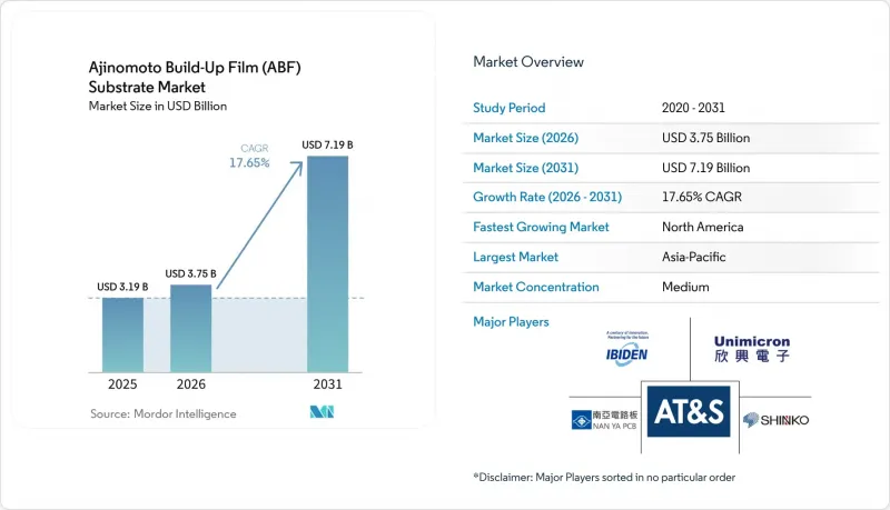
味之素的積層製造膜基板市場預計將從 2025 年的 31.9 億美元和 2026 年的 37.5 億美元成長到 2031 年的 71.9 億美元,2026 年至 2031 年的年複合成長率(CAGR)為 17.65%。
本報告依封裝類型(覆晶BGA、覆晶CSP)、應用領域(AI GPU、CPU、AI加速器、網路IC)、終端用戶產業(資料中心、家用電子電器、汽車、電信)及地區(北美、歐洲、亞太地區及世界其他地區)進行細分。市場預測以美元計價。
全球味之素積層製造膜(ABF)基板市場趨勢及洞察
AI GPU封裝中ABF基板的應用日益廣泛
NVIDIA H200 和 AMD MI300 等新一代 AI GPU 需要 12 至 20 層堆疊層、小於 15µm 的線間距以及小於 2 ppm/ 度C的熱膨脹係數 (CTE) 來減少翹曲,這使得味之素堆疊膜 (ABF)基板的需求達到了歷史新高。IBIDEN已決定在日本投資 5,000 億日圓(約 33 億美元)建造兩座晶圓廠,計劃於 2027 會計年度陸續開始量產,而這些 GPU 正是其明確的目標產品。在多晶片封裝佈局中,每個封裝的基板面積加倍。味之素控制 ABF 介質膜 95% 以上的供應量,並宣布將在 2030 年前將其產能提高 50%,以滿足這一需求。由於認證需要一年以上的前置作業時間,預計供應至少在 2027 年之前都會保持緊張狀態,這使得領先參與企業擁有定價權。
向晶片組架構過渡需要大面積基板
分散式運算單元(例如AMD的「Bergamo」和英特爾的「Meteor Lake」中的單元)顯著增加了基板面積,增幅達40%至60%,需要每平方毫米2000個網的佈線密度以及多達24層的基板。這種設計複雜性的增加促使南亞印刷電路板等製造商開發出24層或更多層的基板,目標是2026年實現小於15微米的精細結構。然而,隨著多個高價值晶片整合到單一多層基板上,單一致命缺陷所帶來的經濟風險也顯著增加。為了降低這種風險,供應商正在採用先進技術,例如前饋自適應微影術和高速光學檢測系統。這些措施旨在早期檢測並解決製造過程中的顆粒和殘留物等問題,尤其是在多層化階段之前,確保更高的良率和可靠性。
高資本密集度和較長的設備採購前置作業時間
待開發區建廠需要8億至12億美元的投資,而購買雷射鑽孔機和真空貼合機等關鍵設備可能需要12至18個月的等待期。這些高成本和漫長的交付前置作業時間有效地將規模小規模的新參與企業拒之門外。安姆科公司位於亞利桑那州的工廠就是一個典型的例子,該工廠於2025年底開工。儘管根據《晶片製造和創新法案》(CHIPS Act)獲得了4.07億美元的津貼,但該工廠直到2028年初才實現盈利,這凸顯了此類項目漫長的前置作業時間。此外,寡占的設備供應商往往優先考慮現有客戶。這種做法為新參與企業帶來了高昂的成本和供應鏈的挑戰,進一步加深了該產業的進入門檻。
細分市場分析
預計到2025年,味之素用於FC-BGA的增材膜將佔據88%的市場佔有率,並以18.05%的複合年成長率成長,與該細分市場的整體成長趨勢相近。 FC-BGA是人工智慧加速器和伺服器CPU的關鍵技術,它能最大限度地降低電感,並實現直接焊料凸塊互連,支援超過10,000個訊號。IBIDEN的川間和大野工廠已全面投入生產用於人工智慧伺服器的FC-BGA產品。隨著三星馬達的產品在2025年通過AEC-Q100認證,該公司有望抓住市場對區域ECU日益成長的需求。
剩餘的市場佔有率由光纖通道半導體光處理器(FC-CSP)佔據,這些光處理器主要供應行動裝置和穿戴式裝置。在這些領域,物理高度限制比單純的頻寬性能更為重要。隨著半導體資本投資擴大轉向對效能和頻寬要求更高的資料中心,FC-CSP 的出貨量成長受到限制。然而,FC-CSP 在支援熱設計功耗(TDP)低於 20W 的邊緣人工智慧系統晶片(SoC)方面仍然發揮著至關重要的作用。該領域的供應商利用成熟的 15-20 微米設計規則,在滿足這些應用特定需求的同時,也保持了成本效益的競爭優勢。
區域分析
預計亞太地區將主導市場,到2025年將佔據58%的市場。台灣的Unimicron、南亞PCB和Kinsus等公司策略性地圍繞台積電的CoWoS生產線佈局,推動著該地區的成長。儘管Kinsus已投資7.44億美元用於擴張,但短期供應缺口仍存在,使該地區面臨供應中斷的風險。地緣政治緊張局勢或地震等天災可能導致6至12個月的供應中斷。日本也是該地區的主要參與者, IBIDEN和Shinkoh兩家公司共投資5,600億日圓(約37.5億美元)以維持其在國內的高科技優勢。同時,韓國的三星馬達和LG Innotek正在越南投資,以利用其低廉的人事費用,同時保持其作為技術安全隔離網閘的地位。
儘管北美市場基數較小,但預計將以18.65%的複合年成長率實現最快成長。 《晶片製造和整合產品法案》(CHIPS Act)提供了大量津貼,其中包括向安姆科(Amcor)提供的4.07億美元和向阿布索利克斯(Absolix)提供的7500萬美元,這充分體現了政府對該行業的大力支持。然而,待開發區案的投資回收期較長仍是一大挑戰。一旦國內基板生產線獲得認證,像TTM Technologies這樣的公司將有望從中受益。此外,超大規模資料中心業者正擴大將北美供應商納入其雙重採購策略,這將進一步提升該地區的成長潛力。
歐洲在市場上佔據獨特的利基地位,AT&S在奧地利投資5億歐元(5.4億美元)建立的能力中心便是最好的例證。該地區受益於對ISO 26262和IATF 16949等高品質標準的需求,尤其是來自汽車OEM廠商和工業自動化公司的需求。這些嚴格的要求有助於本地供應商抵禦來自成本更低的亞洲製造商的競爭。同時,在三星和Meiko等公司的投資推動下,越南正崛起為重要的組裝中心。相較之下,南美和中東目前僅佔很小的市場佔有率,且這些地區的業務活動有限。
其他好處:
- Excel格式的市場預測(ME)表
- 3個月的分析師支持
目錄
第1章:引言
- 研究假設和市場定義
- 調查範圍
第2章:調查方法
第3章執行摘要
第4章 市場狀況
- 市場概覽
- 市場促進因素
- AI GPU封裝中ABF基板的應用日益廣泛
- 向晶片組架構過渡需要大面積基板
- 台灣和日本的主要基板製造商正在擴大產能。
- 先進的微影術整合技術,可實現小於10µm的線寬和間距。
- 與超大規模資料中心業者簽訂策略性長期供應協議
- 根據《CHIPS法案》及類似法律,位置激勵措施
- 市場限制因素
- 資本密集度高,設備前置作業時間長
- 堆疊 10 層或更多層時,工藝良率面臨挑戰
- 積極的產能擴張會帶來短期供應過剩的風險。
- 替代玻璃和 RDL 優先基板技術的出現。
- 宏觀經濟因素對市場的影響
- 產業價值鏈分析
- 監理情勢
- 技術展望
- 波特五力分析
第5章 市場規模與成長預測
- 按包裝類型
- 覆晶BGA
- 覆晶CSP
- 透過使用
- 用於人工智慧的GPU
- CPU(伺服器和桌上型電腦)
- AI加速器(TPU、NPU、客製化ASIC)
- 網路/資料中心積體電路
- 按最終用戶行業分類
- 資料中心/雲端資料中心
- 家用電子產品
- 汽車(ADAS、自動駕駛計算)
- 通訊與網路
- 按地區
- 北美洲
- 歐洲
- 亞太地區
- 世界其他地區
第6章 競爭情勢
- 市場集中度
- 策略趨勢
- 市佔率分析
- 公司簡介
- Ibiden Co., Ltd.
- Unimicron Technology Corp.
- Nan Ya Printed Circuit Board Corporation
- Shinko Electric Industries Co., Ltd.
- Kinsus Interconnect Technology Corp.
- AT&S Austria Technologie & Systemtechnik AG
- Kyocera Corporation
- LG Innotek Co., Ltd.
- Samsung Electro-Mechanics Co., Ltd.
- TTM Technologies, Inc.
- Shennan Circuits Co., Ltd.
- Zhen Ding Technology Holding Limited
- DSBJ Co., Ltd.
- Isu Petasys Co., Ltd.
- NCAB Group AB
- Meiko Electronics Co., Ltd.
- Wus Printed Circuit Company Limited
- Yokowo Co., Ltd.
- Daeduck Electronics Co., Ltd.
- Ebina Denka Kogyo Co., Ltd.
第7章 市場機會與未來展望
According to Mordor Intelligence, the ajinomoto build-Up film substrate market size is projected to expand from USD 3.19 billion in 2025 and USD 3.75 billion in 2026 to USD 7.19 billion by 2031, registering a 17.65% CAGR between 2026 and 2031.
This report is Segmented by Package Type (Flip-Chip BGA, and Flip-Chip CSP), Application (AI GPUs, Cpus, AI Accelerators, and Networking ICs), End-User Industry (Data Centers, Consumer Electronics, Automotive, and Telecom), and Geography (North America, Europe, Asia-Pacific, and Rest of the World). Market Forecasts are Provided in Terms of Value (USD).
Global Ajinomoto Build-Up Film (ABF) Substrate Market Trends and Insights
Rising Adoption Of ABF Substrates In AI GPU Packages
Next-generation AI GPUs such as NVIDIA H200 and AMD MI300 require 12-to-20 build-up layers, sub-15 µm lines and spaces, and coefficient of thermal expansion (CTE) matching within 2 ppm / °C to mitigate warpage, pushing Ajinomoto Build-Up Film substrate market demand to record highs. Ibiden earmarked JPY 500 billion (USD 3.3 billion) for two Japanese fabs that will begin sequential ramp in fiscal 2027, explicitly aimed at these GPUs. Multi-chiplet layouts double the substrate area per package, and Ajinomoto, which controls over 95% of the ABF dielectric film supply, has announced a 50% capacity increase by 2030 to keep pace. With qualification lead times longer than a year, supply stays tight through at least 2027, granting early movers pricing power.
Shift Toward Chiplet Architectures Requiring Large-Area Substrates
Disaggregated compute tiles in AMD Bergamo or Intel Meteor Lake significantly increase substrate real estate by 40-60%, creating a need for routing densities of 2,000 nets/mm2 and up to 24 layers. This increase in design complexity has driven manufacturers like Nan Ya Printed Circuit Board to develop 24-plus-layer substrates that aim to achieve sub-15 µm geometries by 2026. However, as multiple high-value dice are integrated onto a single laminate, the economic risk associated with a single killer defect rises substantially. To mitigate this risk, suppliers are adopting advanced technologies such as feed-forward adaptive lithography and high-speed optical inspection systems. These measures are designed to detect and address issues like particles or residue early in the production process, specifically before the lamination stage, ensuring higher yields and improved reliability.
High Capital Intensity And Long Equipment Lead Times
Greenfield fabs require investments ranging from USD 800 million to USD 1.2 billion and face a 12-18 month wait to procure essential equipment, such as laser drillers or vacuum laminators. These high costs and extended timelines effectively exclude smaller entrants from competing in the market. A case in point is Amkor's Arizona plant, where construction commenced in late 2025. Despite receiving USD 407 million in CHIPS funding, the facility only began generating revenue in the first half of 2028, highlighting the lengthy lead times associated with such projects. Additionally, tool vendors, which operate as oligopolies, tend to prioritize their established customers. This practice creates high cost and supply chain challenges for new market entrants, further solidifying the barriers to entry in this space.
Other drivers and restraints analyzed in the detailed report include:
- Capacity Expansion Of Leading Substrate Makers In Taiwan And Japan
- Advanced Lithography Integration For Sub-10 µm Lines And Spaces
- Process Yield Challenges Above 10 Build-Up Layers
For complete list of drivers and restraints, kindly check the Table Of Contents.
Segment Analysis
The Ajinomoto Build-Up Film market size for FC-BGA accounted for 88% in 2025 and is expected to grow at a 18.05% CAGR alongside the overall segment. FC-BGA enables direct solder bump interconnects that minimize inductance and support >10,000 signals, indispensable for AI accelerators and server CPUs. Ibiden's Kawama and Ohno plants are fully dedicated to FC-BGA lines aimed at AI servers. Automotive-qualified versions passed AEC-Q100 in 2025, positioning Samsung Electro-Mechanics to capture rising zonal ECU demand.
FC-CSP held the remaining share, primarily catering to mobiles and wearables, where physical height constraints take precedence over raw bandwidth capabilities. The growth in FC-CSP volume is limited as semiconductor capital investments increasingly shift focus toward data centers, which demand higher performance and bandwidth. However, FC-CSP continues to play a significant role in supporting edge AI SOCs with TDPs under 20 W. Suppliers in this segment capitalize on well-established, mature 15-20 µm design rules, enabling them to maintain a competitive edge in cost efficiency while addressing the specific needs of these applications.
Geography Analysis
Asia-Pacific is expected to dominate the market, accounting for 58% of the 2025 value. Taiwan's Unimicron, Nan Ya PCB, and Kinsus are strategically clustered around TSMC CoWoS lines, driving regional growth. Despite Kinsus' USD 744 million expansion efforts, the near-term supply gap persists, leaving the region vulnerable to disruptions. Any geopolitical tensions or natural disasters, such as earthquakes, could potentially erase 6-12 months of supply. Japan is also a key player in the region, with Ibiden and Shinko investing a combined JPY 560 billion (USD 3.75 billion) to maintain high-layer technology expertise locally. Meanwhile, South Korea's Samsung Electro-Mechanics and LG Innotek are channeling investments into Vietnam to leverage lower labor costs, although they continue to act as technology gatekeepers.
North America, although starting from a smaller base, is projected to experience the fastest growth with a compound annual growth rate (CAGR) of 18.65%. The CHIPS Act has provided significant grants, including USD 407 million to Amkor and USD 75 million to Absolics, signaling strong governmental support for the sector. However, the long payback period for greenfield projects remains a challenge. Companies like TTM Technologies are poised to benefit once domestic substrate lines achieve qualification. Additionally, hyperscalers are increasingly incorporating North American suppliers into their dual-sourcing strategies, further boosting the region's potential for growth.
Europe maintains a niche position in the market, led by AT&S's EUR 500 million (USD 540 million) competence center in Austria. The region benefits from the demand for high-quality standards such as ISO 26262 and IATF 16949, particularly from automotive OEMs and industrial automation players. These stringent requirements help shield local suppliers from competition with low-cost Asian manufacturers. Elsewhere, Vietnam is emerging as a significant assembly hub, driven by investments from companies like Samsung and Meiko. In contrast, South America and the Middle East currently hold negligible positions in the market, with limited activity in these regions.
- Ibiden Co., Ltd.
- Unimicron Technology Corp.
- Nan Ya Printed Circuit Board Corporation
- Shinko Electric Industries Co., Ltd.
- Kinsus Interconnect Technology Corp.
- AT&S Austria Technologie & Systemtechnik AG
- Kyocera Corporation
- LG Innotek Co., Ltd.
- Samsung Electro-Mechanics Co., Ltd.
- TTM Technologies, Inc.
- Shennan Circuits Co., Ltd.
- Zhen Ding Technology Holding Limited
- DSBJ Co., Ltd.
- Isu Petasys Co., Ltd.
- NCAB Group AB
- Meiko Electronics Co., Ltd.
- Wus Printed Circuit Company Limited
- Yokowo Co., Ltd.
- Daeduck Electronics Co., Ltd.
- Ebina Denka Kogyo Co., Ltd.
Additional Benefits:
- The market estimate (ME) sheet in Excel format
- 3 months of analyst support
TABLE OF CONTENTS
1 INTRODUCTION
- 1.1 Study Assumptions and Market Definition
- 1.2 Scope of the Study
2 RESEARCH METHODOLOGY
3 EXECUTIVE SUMMARY
4 MARKET LANDSCAPE
- 4.1 Market Overview
- 4.2 Market Drivers
- 4.2.1 Rising Adoption of ABF Substrates in AI GPU Packages
- 4.2.2 Shift Toward Chiplet Architectures Requiring Large-Area Substrates
- 4.2.3 Capacity Expansion of Leading Substrate Makers in Taiwan and Japan
- 4.2.4 Advanced Lithography Integration for Sub-10 µm Lines and Spaces
- 4.2.5 Strategic Long-Term Supply Agreements With Hyperscalers
- 4.2.6 Localization Incentives Under CHIPS and Similar Acts
- 4.3 Market Restraints
- 4.3.1 High Capital Intensity and Long Equipment Lead Times
- 4.3.2 Process Yield Challenges Above 10 Build-Up Layers
- 4.3.3 Short-Term Oversupply Risk From Aggressive Capacity Adds
- 4.3.4 Emergence of Alternative Glass and RDL-First Substrate Technologies
- 4.4 Impact of Macroeconomic Factors on the Market
- 4.5 Industry Value Chain Analysis
- 4.6 Regulatory Landscape
- 4.7 Technological Outlook
- 4.8 Porter's Five Forces Analysis
- 4.8.1 Bargaining Power of Suppliers
- 4.8.2 Bargaining Power of Buyers
- 4.8.3 Threat of New Entrants
- 4.8.4 Threat of Substitutes
- 4.8.5 Degree of Competition
5 MARKET SIZE AND GROWTH FORECASTS (VALUE)
- 5.1 By Package Type
- 5.1.1 Flip-chip BGA
- 5.1.2 Flip-chip CSP
- 5.2 By Application
- 5.2.1 AI GPUs
- 5.2.2 CPUs (Server and Desktop)
- 5.2.3 AI Accelerators (TPUs, NPUs, Custom ASICs)
- 5.2.4 Networking / Data Center ICs
- 5.3 By End-user Industry
- 5.3.1 Data Centers / Cloud
- 5.3.2 Consumer Electronics
- 5.3.3 Automotive (ADAS, Autonomous Compute)
- 5.3.4 Telecom and Networking
- 5.4 By Geography
- 5.4.1 North America
- 5.4.2 Europe
- 5.4.3 Asia-Pacific
- 5.4.4 Rest of the World
6 COMPETITIVE LANDSCAPE
- 6.1 Market Concentration
- 6.2 Strategic Moves
- 6.3 Market Share Analysis
- 6.4 Company Profiles (includes Global Level Overview, Market Level Overview, Core Segments, Financials as available, Strategic Information, Market Rank/Share, Products and Services, Recent Developments)
- 6.4.1 Ibiden Co., Ltd.
- 6.4.2 Unimicron Technology Corp.
- 6.4.3 Nan Ya Printed Circuit Board Corporation
- 6.4.4 Shinko Electric Industries Co., Ltd.
- 6.4.5 Kinsus Interconnect Technology Corp.
- 6.4.6 AT&S Austria Technologie & Systemtechnik AG
- 6.4.7 Kyocera Corporation
- 6.4.8 LG Innotek Co., Ltd.
- 6.4.9 Samsung Electro-Mechanics Co., Ltd.
- 6.4.10 TTM Technologies, Inc.
- 6.4.11 Shennan Circuits Co., Ltd.
- 6.4.12 Zhen Ding Technology Holding Limited
- 6.4.13 DSBJ Co., Ltd.
- 6.4.14 Isu Petasys Co., Ltd.
- 6.4.15 NCAB Group AB
- 6.4.16 Meiko Electronics Co., Ltd.
- 6.4.17 Wus Printed Circuit Company Limited
- 6.4.18 Yokowo Co., Ltd.
- 6.4.19 Daeduck Electronics Co., Ltd.
- 6.4.20 Ebina Denka Kogyo Co., Ltd.
7 MARKET OPPORTUNITIES AND FUTURE OUTLOOK
- 7.1 White-Space and Unmet-Need Assessment
 2026年全球碳化矽(SiC)單晶基板市場報告
 軟式電路板市場規模、佔有率和趨勢分析報告:按材料、類型、應用、最終用途、地區和細分市場分類(2026-2033 年)
 味之素積層製造膜全球市場:按應用和地區分類 - 預測至 2032 年
 《全球氮化鋁單晶基板銷售市場報告:競爭分析與區域機會(2026-2032)》
 先進基板材料市場預測至2034年—按材料類型、基板類型、平台、技術、應用、最終用戶和地區分類的全球分析2026年全球氧化鎂板市場報告
 5G基板材料市場:依產品類型、材料類型、應用和最終用戶產業分類-2026-2032年全球市場預測
 半導體晶圓回收:市場佔有率分析、產業趨勢與統計、成長預測(2026-2031)軟式電路板市場:依材料、技術、厚度、應用和終端用戶產業分類,全球預測(2026-2032年)鑽石基板市場:按類型、尺寸、沉積技術、純度等級、應用和最終用戶分類-2026年至2032年全球預測